國
立
交
通
大
學
電子工程學系電子研究所
碩
士
論
文
鎳鐵與氧化鋁奈米複合材料的合成及製程開發使螺
旋電感的性能增強
Material Synthesis and Process Development of NiFe-AAO
Nanocomposite for Performance Enhancement of On-chip Spiral
Inductor
研 究 生:許欣富
指導教授:鄭裕庭 教授
鎳鐵與氧化鋁奈米複合材料的合成及製程開發使螺旋電感的性能
增強
Material Synthesis and Process Development of NiFe-AAO
Nanocomposite for Performance Enhancement of On-chip Spiral
Inductor
研 究 生:許欣富 Student:Hsin-Fu Hsu 指導教授:鄭裕庭 Advisor:Yu-Ting Cheng 國 立 交 通 大 學 電子工程學系電子研究所 碩 士 論 文 A ThesisSubmitted to Department of Electronics Engineering & Institute of Electronics College of Electrical and Computer Engineering
National Chiao Tung University in partial Fulfillment of the Requirements
for the Degree of Master
in
Electronics Engineering
Sep 2009
Hsinchu, Taiwan, Republic of China
i
鎳鐵與氧化鋁奈米複合材料的合成及製程開發使螺旋電感
的性能增強
學生:許欣富 指導教授:鄭裕庭 教授 國立交通大學電子工程學系暨電子研究所碩士班摘
要
在 此 篇 論 文 中 , 我 們 使 用 奈 米 鎳 鐵 柱 應 用 於 高 頻 螺 旋 電 感 , 利 用 空 間 中 相 對 磁 導 率 的 提 升 來 增 加 電 感 值 , 以 達 到 無 線 通 訊 應 用 晶 片 面 積 微 小 化 的 目 標 。 直 徑 7 0 n m , 高 度 1 μ m 的 奈 米 鎳 鐵 柱 是 利 用 沉 積 在 矽 基 板 上 的 陽 極 氧 化 鋁 模 板 以 電 鍍 方 法 所 製 成 , 規 則 的 奈 米 鎳 柱 陣 列 被 高 電 阻 率 的 陽 極 氧 化 鋁 模 板 所 分 隔 , 有 效 的 避 免 了 電 感 在 高 頻 應 用 時 所 產 生 在 磁 性 材 料 的 渦 電 流損耗。在本實驗設計中,奈米鎳柱應用於螺旋電感,觀察奈米鎳柱鐵芯受到電感均勻 的磁場磁化下,所得到的奈米鎳柱鐵芯電感高頻特性。最後,已完成的四圈半奈米鎳柱 鐵芯螺旋電感的高頻特性被量測由 0.1GHz 到 5GHz,電感值約有 23 % 的增加,持續到 達 1GHz 為止。
ii
Material Synthesis and Process Development of NiFe-AAO
Nanocomposite for Performance Enhancement of On-chip
Spiral Inductor
Student:Hsin-Fu Hsu Advisor:Dr. Yu-Ting Cheng
Department of Electronics Engineering & Institute of Electronics National Chiao Tung University
Abstract
This thesis presented a fully CMOS compatible process to implement NiFe (68 at%. Ni and 32 at.% Fe) –AAO nanocomposite as magnetic core material for on-chip spiral inductor fabrication. The NiFe nanorod arrays with 60~70 nm diameter using DC electroplated are deposited and electrically isolated in anodic alumina oxide (AAO) template on silicon substrate. Experimental results show that the spiral inductor of 4.5 turns using NiFe-AAO nanocomposite magnetic core can have 23% inductance enhancement than that of inductor without the core up to 1 GHz.
iii
誌
謝
學長們總說:兩年一下就過了啦,撐一下,果然,轉眼間,碩士生涯就 結束了,有苦有樂,苦的是實驗的迴圈,樂的是…身在 MIL。畢業了,當然 首先感謝的是家人,在我在學的兩年多一點點,在心靈層面,給了我很大 的支持,讓我可以心無旁騖的專注在實驗與課業上,感謝我的父母與姊姊 們! 在交大的兩年,很感謝我的指導教授-鄭裕庭老師,讓我了解-如何從 不同角度觀察事物,也讓我提早了解到社會的現實性。 接下來,頒發特別感謝獎,得獎的是每年都獲獎的子元大大(希望是最後 一年有人感謝你了),如果沒有你的帶領,你犀利的針對問題,我想…我可 能要晚好幾個月寫致謝,XDXD,真是大恩不言謝!感謝健章大大,在理論 上給我一定的支持,不吝嗇花你寶貴的時間為我解惑,中央出品的,果然 都是好貨色,哈哈,甘恩喔!實驗室竄起的新勢力-昌博,本來以為你明年 就會去當兵的,沒想到讓你矇到了,科科,感謝你陪我一起做實驗,給了 我很多建議,不論是實驗還是玩樂,也常常幫我修電腦,我跟你去夜市的 次數,比跟我女朋友還多,你就知道你的重要性了(>///<),希望你可以四 年就畢業!ㄜ…還是要感謝一下在印度擠牛奶的辛杰瑞先生,教了我一些 外國的風情與語言…喔,還有讓阿昌踩了一下!住在我家附近的小筑,但 是好像才來我家吃過一次早餐(?),感謝你為我們處理了很多雜物,身為 MIL 中唯一的女生,有妳的存在,讓實驗室的氣氛很不同,出遊也替我們增色 不少,希望妳工作愉快~ 坐在我右手邊的倫豪(學長),幫我拍了很多 SEM,,感謝你陪我一起打球, 聽我抱怨實驗的不順,與我同寢一年(但大概只有半年在吧),希望你兵旅 順利,你人很 nice 的,我知道你會說“沒有啦”!常常被我虧的小家,你 也知道,我講話很直的,但是有時候會有點過頭,希望你別在意,感謝你 兩年的陪伴,一直被我跟倫豪攻擊,真是委屈你了,希望你可以在十月順 利畢業!也感謝你讓我住在你家很久,房東,要繳械了嗎? 講話也很直,很大聲的冠名,雖然我第一次見到你,覺得你很機八,但 我知道你很有義氣,心思又縝密,在我熬夜時為我送上咖啡,感謝你陪我 一起共度 AAO 的時光;李茶…喔不是,奎豬,感謝你替我們安排出遊的行 程,雖然還沒成行,科科,我知道你是個乖小孩,竹中畢業的,都不是那 麼容易被打倒的,加油!奇怪,老師怎麼只有收兩個?喔…還有個光頭(腦 哥?),我只能說…你很天兵,希望你可以保持你的童貞到畢業!(你們在找 -單面雙面膠嗎?) 當然也要感謝-茄子,希望你的出國行順利阿!還有奶瓶與衛斯理學 長,希望你們可以順利登出國軍! 按照慣例,最後最後,感謝蔡小柔,YAYA!!
iv
Contents
摘要……… i Abstract………... ii 致 謝…… ……… ……… ……… ……… ……… ……… ……… …… … iii Content……… iv Figure Captions.………... v Table Captions……… vi Chapter 1 Introduction ... 1Chapter 2 Experimental Setup ... 5
2.1 NiFe-AAO Nanocomposite Synthesis and Characterization ... 5
2.2 Nickel nanorod Arrays ... 10
Chapter 3 Result and Discussion ... 13
Chapter 4 Conclusion and Future Work ... 21
Reference ... 22
v
Figure Captions
Chapter1
Fig.1-1.Schematic representation of the 3.5 turns spiral inductors with the Ni nanorods core ... 1
Chapter 2
Fig.2-1. Anodization process flow. ... 5 Fig.2-2.The SEM image of AAO template with 70 nm pore diameter. ... 6 Fig.2-3. SEM photographs of NiFe Nanorods of (a) top view (b) cross section. . 8 Fig.2-4. M-H loops of NiFe-AAO nanocomposite with different form of applied magnetic fields. (a) in-plane. (b) out-of-plane. ... 9 Fig.2-5. Schematic of the inductors with the NiFe nanorods core fabrication processes ... 11 Fig.2-6. SEM photograph of as-fabricated on chip spiral inductors with
NiFe-AAO nanocomposite. ... 12
Chapter 3
Fig.3-1.Inductance and Q-factor measurement of the 3.5,4.5 turns inductors ... 15 Fig.3-2. The O concentration profile determined by SIMS ... 14 Fig.3-3. The S11 parameter of the 3.5 turns inductor ... 19 Fig.3-4. The S11 parameter of the 4.5 turns inductor ... 20
vi
Table Captions
Chapter 1
Table.1-1.The introduction of some ferromagnetic inductor approaches. ... 4
Chapter 2
Table.2-1. Characteristics of NiFe electrolyte………5
Chapter 3
1
Chapter 1 Introduction
One of the technical challenges in the cost reduction of RFIC (Radio Frequency Integrated Circuit) for consumer electronic applications is inevitable large area occupation of RF on-chip passive components, such as inductor, capacitor, and filter…etc. For instance, inductor for GHz RFIC operation ranging from 1.5 to 3.5 nH can have the size of 0.06 to 0.08 µm2 [1]. The larger size the inductor is, the higher inductance it can have. In addition, it is required to have least three inductors for a second order bandpass filter design whose size will be up to 0.62 mm2 at least [2]. Thus, high-k and ferromagnetic materials have been synthesized and developed to increase the capacitance and inductance per area, respectively, in the development of radio frequency integrated circuit (RFIC) technology in recent years. In this thesis, a new ferromagnetic composite material is synthesized for enhancing inductor performance.
Previously, Viala et al. demonstrated the coplanar ferromagnetic inductor with a 15% increase in inductance using solid magnetic (CoZrNb) alloy [3]. Kim et al. proposed on-chip solenoid inductors incorporated with Fe3O4 magnetite nanorod
cores for having higher inductance [4]. Jiang et al. employed exchange-coupled characteristic of antiferromagnetic/ferromagnetic multilayers (IrMn/CoFe) to enhance inductance up to 20% without having any Q preference degradation [5]. Table 1-1 introduces these approaches about the inductors with magnetic material core in RF range application. Although these approaches can indeed achieve the inductance enhancement, the enhancement which only occurs in MHz range and is realized with CMOS-incompatible material and processes is not practical in real CMOS on-chip spiral inductor fabrication. Thus, our group
2
developed a new composite material with CMOS compatible fabrication process that is electroless deposited Ni-AAO (anodic alumina oxide) nanocomposite. Using the composite as magnetic core material, inductance enhancement can be realized up to 5.3 GHz [6]. Fig.1. shows the representation of the 3.5turns spiral inductors with the Ni Nanorods core.
Fig.1-1.Schematic representation of the 3.5 turns spiral inductors with the Ni nanorods core
Nevertheless, it has been found that such an electroless Ni-P alloy has strong relation to its P content in terms of magnetic property and the saturated magnetization of Ni-P is less than that of a pure Ni [7]. According to Weiss theory [8], P incorporation would result in the interatomic distance enlargement
of Ni which can cause exchange force reduction. Since the force reduction would make the permeability of Ni-P smaller than that of pure Ni [7], only 3% inductance enhancement is observed so far in the inductor using the Ni-AAO nanocomposite as the magnetic core. Meanwhile, ferromagnetic resonance (FMR) frequency (FMR) is expressed as γ/2π[Hk (Hk + 4πMs)], where γ is the
3
magnetization. To effectively elevate the FMR frequency well above several gigahertz ranges for practical application to RFIC using the inductor with ferromagnetic core, it is required further study to improve material characteristics such as Hk and Ms.
Previous study has shown that the rod like shape and nanometer size of magnetic material could have higher anisotropy field Hk [9]. Thus, in this thesis,
a NiFe-AAO nanocomposite with fully CMOS-compatible process will be developed for on-chip spiral inductors fabrication. Because NiFe has larger permeability and saturation magnetization than that of Ni and has a form of nanorod in the composite system, material characterization, better inductor performance can be expected.
Table.1-1.The introduction of some ferromagnetic inductor approaches. RF plane
ferromagnetic inductors on silicon (2004) [3]
Magnetite (Fe3O4) nanorod cores for Integrated Solenoid RF Inductors (2006) [4] Exchange-Coupled IrMn/CoFe Mulitayers for RF Integrated Inductors (2007) [5] L enhancement (%) @ application frequency L = 4.2nH (+15%) at 1.2GHz L = 2.63nH (+3.5%) at 3GHz L = 3.8nH (+30%) at 1.8GHz Q variation (%) @ useful frequency Q = 10 (-35%) at 1GHz Q = 2.9 (-3%) at 3GHz Q = 6.5 (+0%) at 1.8GHz
4 Q peak variation @ frequency Q = 23 at 5GHz Q = 11 at 1.2GHz Q = 9.5 at 13GHz Q = 7 at 11GHz Q = 6.3 at 2GHz Q = 6.3 at 1.7GHz (fFMR) Ferromagnetic resonance frequency 2.5GHz (strong absorbability) 5GHz (weak absorbability) 4.3GHz (strong absorbability) Air core (fLc) Self-resonant Frequency N/A ~ ( >8GHz ) 17GHz 5GHz
Magnetic material CoZrNb Fe3O4 nanorod CoFe
Structure and design Solid magnetic plane Magnetic material in core IrMn/CoFe Mulitayers
5
Chapter 2 Experimental Setup
2.1 NiFe-AAO Nanocomposite Synthesis and Characterization
In comparison with the previous developed electroless deposited Ni-AAO nanocomposite process, the synthesis of NiFe-AAO nanocomposite requires a seed layer under AAO layer. Thus, a Ti (200 nm)/Al (1000 nm) layer is e-beam deposited on a 4” silicon substrate grown with a layer of 0.2 um thermal oxide as electrical isolation layer. Then, the AAO template is fabricated by applying a constant voltage 40V to the substrate in a 0.3 M oxalic acid (H2C2O4) solution at
2℃. The low temperature anodization process can reduce excessive current flow and heat evolution to make the AAO with the characteristics of small-pore films [12]. Fig.2-1. shows the process flow.
(a) Al film deposition (b) Anodization (c) Pore Widening Treatment Fig.2-1. Anodization process flow.
Once the film is anodized, the voltage is reduced from 40V to 15V with a rate of 0.11V/s and then kept for 15mins for thinning the alumina oxide barrier layer. The insulting barrier layer is then further thinned to completely anodized Al film by applied a reversed-bias voltage (-2.2V) to the substrate in a 0.5M saturated
6
KCL at 2C for 10mins [12, 13]. Finally, the AAO temple is put in a 5% H3PO4
solution at 30C for 25mins to form a uniformly distributed nanopore structure with the size of 70 nm in diameter, shown in Fig.2-2.
Fig.2-2. The SEM image of AAO template with 70 nm pore diameter.
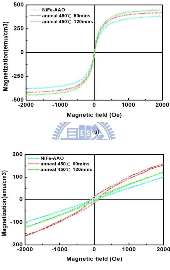
For the synthesis of NiFe-AAO nanocomposite, the as-fabricated AAO temple is DC electroplated in a Ni sulfate based NiFe bath with the formulation listed in Table 2-1 [14]. The plating conditions are 28C and 0.035A/mm2 current density. Fig. 2-3 shows the as-deposited NiFe-AAO nanocomposite. NiFe nanorods are grown within the AAO matrix. Fig.2-4. shows the superconducting quantum interference device (SQUID) measurements of NiFe-AAO nanocomposite; the applied field directions are in plane and out plane. The slope of the M-H curve exhibits the relative permeability, the larger slope lead to the larger permeability. The relative permeability can be calculated as follows:
0
4
1
H
M
r
(1)where M is magnetization and H0 is the applied magnetic field. The relative
7
applied field (at 100 Oe). In addition, the FMR frequency of ferromagnetic film is estimated about as high as 5.72 GHz due to large Hk, which is about 800 Oe.
Compound Concentration Nickel sulfate (g/l) 200 Iron sulfate (g/l) 8 Nickel chloride (g/l) 5 Boric acid (g/l) 25 Saccharin (g/l) 2 Sodium lauryl sulfate 1 cm (g/l) 0.1 Deposition temperature (℃) 28 PH 3 Table 2-1
8
(a)
(b)
9
(a)
(b)
Fig. 2-4. M-H loops of NiFe-AAO nanocomposite with different form of applied magnetic fields. (a) in-plane. (b) out-of-plane.
10
2.2
Inductor FabricationThe spiral inductors of 3.5 and 4.5 turns, that are made of 5-um-thick electroplated Cu and designed with 100 um in inner diameter, 15 um in line width, and 5 um in line space have been utilized for the investigation of inductance enhancement using NiFe-AAO nanocomposite as a magnetic core. Fig.5 illustrates the fabrication process of the on–chip spiral inductors with NiFe nanorods. It begins with wet oxidation at 1050℃ for 0.75 um of thermal oxide, followed by electron-beam-evaporated Ti/Al (0.2 um/1um) deposition on the p-type silicon substrate as shown in Fig.2-5(a), and then AAO template is fabricated using the aforementioned as shown in Fig.2-5(b). The NiFe nanorod arrays were then deposited by DC electroplating shown in Fig.2-5(c). Once the magnetic layer is fabricated, as Fig.2-5(d) shows, a layer of 0.2-um-thick-SiO2 is sputtered on the top of the composite film as an electrical
insulation layer followed by the first thin Cr/Cu (500Å /1000Å ) adhesion/seed layer deposition. For the inductor fabrication, a 6um thick AZ 4620 photo-resist is patterned to define the region for coil fabrication of spiral inductor, as shown in Fig.2-5(e). After the first layer of 5-um-thick Cu plating, another 10um thick AZ 4620 is spun, patterned, and sputtered with 150nm Cu seed layer for the via filling of Cu as shown in Fig.2-5(f). Fig.2-5(g) shows another 10-um AZ 4620 is spun onto the plated structure, patterned, and plated with 5um-thick Cu to define air bridge after via filling. At final, the fabrication of the spiral inductor is done right after the Cu seed layer removal, which is chemically etched away using Cu and Cr etchants as shown in Fig.2-5(h). Fig.2-6. shows an as-fabricated 3.5-turn spiral inductor with magnetic
11
NiFe-AAO nanocomposite core.
(a) (b) (c) (d) (e) (f) (g) (h) Silicon Aluminum Silicon dioxide Seed layer Titanium Copper AAO AZ4620 Nickel iron
12
Fig.2-6 SEM photograph of as-fabricated on chip spiral inductors with NiFe-AAO nanocomposite.
13
Chapter 3 Measurement and discussion
In the experiment, the two-port S-parameters of the inductors are measured in the frequency range of 0.5 to 5 GHz with an on-wafer probe station using the high- frequency probes (Cascade Microtech, Inc., ACP-40-GSG-100μm) and Agilent E8364B PNA network analyzer. After short-open-load-through (SOLT) calibration then we can measured the S-parameters. The parasitic parallel capacitance and series contact resistance between the substrate and the contact pads of the inductor are de-embedded via the measurement using well-designed dummy patterns [1]. The de-embedded S parameters are then transformed into Y-parameter using Agilent ADS software. The equivalent series inductance (L) and quality factor (Q) of the inductors are extracted from the Y-parameters base on the following equation [14], respectively:
L = Im(1/Y11 )/2 π f (3)
Q = Im(1/Y11 )/Re(1/Y11 ) (4)
where f is the signal frequency.
The frequency-dependent inductance and Q-factor of the fabricated inductors are depicted in Fig.3-1(a) and (b) shows that the spiral inductor of 3.5 turns with NiFe-AAO nanocomposite magnetic core can have 25% inductance enhancement than that of inductor without the core up to 1 GHz. Meanwhile, the maximum Q-factor (Qm) decreases from 12 to 6 at 1 GHz, which is about 50%
14
case of the spiral inductor of 4.5 turns. The spiral inductor of 4.5 turns with NiFe-AAO nanocomposite magnetic core can have 23% inductance enhancement than that of inductor without the core up to 1 GHz but the Q decreases from 10.3 to 6.4 at 1 GHz, which is about 38% reduction.
In Fig.3-1 (a) and (c), the spiral inductor with NiFe-AAO nanocomposite magnetic core has a capacitance curve trend and has a worse Q-factor than that of inductor without the magnetic core because of the titanium, in the bottom of NiFe-AAO. Titanium is used as the seed layer for NiFe electroplating, but it would result in the effect of parasitic capacitance increase and eddy current loss on the layer of Ti that further cause poor inductance and Q performance. Therefore, it is critical to eliminate the effect resulted by the Ti layer. Previously,
H.H et al. proposed thermal anneal at the temperature higher than 450 ℃ can
make the formation of an amorphous layer at the interface between the Ti and the SiO2. According to the O concentration profile determined by SIMS, it
suggested that this layer was mainly TiOx [15],shown in Fig.3-2.
15
(a)
16
(c)
(d)
Fig.3-1. Measured high-frequency characteristics of spiral inductors with NiFe-AAO nanocomposite core. (a) Inductance of spiral inductor with N=3.5, din=100um. (b) Q-factor of
spiral inductor with N=3.5, din=100um. (c) Inductance of spiral inductor with N=4.5,
17
In order to verify the influence of thermal anneal on the inductor performance, the spiral inductors with NiFe-AAO nanocomposite magnetic core are annealed for two different time periods for 60 minutes and 120 minutes at 450 ℃, respectively. Fig. 8 shows the frequency dependence of the inductance and
Q-factor of the fabricated inductors with NiFe-AAO nanocomposite magnetic
core annealed for 60 minutes and 120 minutes, and the detailed parameter comparison between the inductor with and without thermal anneal samples as listed in Table 3-1. After annealing 60 minutes, the Qm value of the spiral
inductor of 3.5 turns with NiFe-AAO core has increased 10% (from 5.93 to 6.53), and after annealing 120 minutes, the Qm value has increased 60% (from
5.93 to 9.53). Nevertheless, the inductance is accompanied with 4% decrease
N Types(inductor) Inductance enhancement(up to 1 GHz) fQmax(GHz) Qm 3.5 Air-core 1.3 12.1 NiFe-AAO 25% 1 5.93 anneal for 60 minutes 21.2% 1 6.53 anneal for 120 minutes 21.5% 1.1 9.53 4.5 Air-core 1 10.4 NiFe-AAO 23% 1 6.49 anneal for 60 minutes 16.5% 0.7 8.14 anneal for 120 minutes 16.6% 0.8 14.2 Table 3-1
18
(from 25% enhancement to 21% enhancement, up to 1 GHz). Similar Q enhancement and inductance degradation also occur in the case of the spiral inductor of 4.5 turns. After annealing 60 minutes, the Qm value of the spiral
inductor of 4.5 turns with NiFe-AAO core has increased 25% (from 6.49 to 8.14), and after annealing 120 minutes, the Qm value has increased 118% (from
6.49 to 14.2). But, the inductance accompanies with 7% decrease (from 23% enhancement to 16% enhancement, up to 1 GHz), which the magnetic loss due to the higher coercive force (Hc) of the NiFe-AAO nanocomposite after
annealing, as shown in Fig. 2-4.
As aforementioned, the Q degradation originated in the titanium which induced the effect of parasitic capacitance. By annealing to make a part of Ti (titanium) into TiOx, however, Q-factor is a tradeoff of inductance decrease and
magnetic loss. Although there is at least 23% inductance enhancement up 1 GHz in the work, the Q-factor can be further improved by thinning the layer of titanium and annealing enough time for more Ti into TiOx, from a conducting
layer to an insulation layer.Fig.3-3. and Fig.3-4. show the Smith chart of the inductor for S11.
19
20
21
Chapter 4 Conclusion and Future Work
The ferromagnetic inductors using NiFe-AAO nanocomposite as magnetic
core have fabricated. Incorporated with nanocomposite core, the 3.5 and 4.5-turn inductors can have improved inductance up 1 GHz and the nanocomposite (NiFe) has higher saturation magnetization and anisotropy magnetic field enabling a higher FMR frequency. Although the inductance has been effectively enhanced, the effect of capacitance resulted by titanium seed layer could cause the declination of Q that can be improved using thinner titanium or thermal anneal for the formation of titanium oxide for the effect resistance increase of the seed layer .
22
Reference
[1] I. J. Bahl, “High-performance inductors,” IEEE Trans. Microwave Theory
Tech., Vol. 49, No. 4, pp. 654-664, Apr. 2001.
[2] S. Bantas and Y. Koutsoyannopoulos, “CMOS Active-LC Bandpass Filters With Coupled-Inductor Q-Enhancement and Center Frequency Tuning,”
IEEE Trans. On circuits and systemss, VOL. 51, NO. 2, Feb. 2004.
[3] B.Viala, A.S.Royet, R.Cuchet, M.Aid,P.Gaud, O.Valls, M.Ledieu, and O.Acher,“RF plane ferromagnetic inductors on silicon,” IEEE Trans.Magn., vol. 40, no. 4, pp. 1999–2001, July. 2004.
[4] J.Kim, W.Ni,C.Lee,Edwin C.Kan, Ian D.Hosein, Y.Song, and C.Liddell,
“Magnetic property characterization of magnetite (Fe3O4) nanorod cores
for integrated solenoid rf inductors,” J.Appl.Phys 99. 08R903 (2006)
[5] R.F.Jiang,N.N.Shams,M.T.Rahman, and C. H. Lai, “Exchange-coupled IrMn/CoFe mulitlayers for RF-integrated inductors,” IEEE Trans.Magn., vol. 43, no. 10, pp. 3930–3932, Oct. 2007.
[6] M.C.Hsu, T.Y.Chao, Y.T.Cheng,C.M.Liu, and C.Chen, “The inductance enhancement study of spiral inductor using Ni-AAO nanocomposite core,”
IEEE Trans.Nano., vol. 8. no.3, May 2009.
[7] C.C.Hu and A.Bai, “Influences of the phosphorus content on physicochemical properties of nickel–phosphorus deposits, ” Mater. Chem.
Phys. 77 (2002) 215–225.
[8] B.D. Cullity, Introduction to Magnetic Materials, Addison-Wesley, Reading, MA, 1972, pp. 31–136.
[9] N. Cordente, M. Respaud, F. Senocq, M. Casanove, C. Amiens, and B. Chaudret, “Synthesis and magnetic properties of nickel nanorods,”
Nano Lett., vol. 1, pp. 565–568, 2001.
[10] S. Shingubara, “Fabrication of nanomaterials using porous alumina templates,” J. Nanopart. Res., vol. 5, pp. 17–30, 2003.
[11] M. M. Sinha and J. S. Kim, “Analysis of vibrational modes and phonon density of statesof aluminate spinels,” J. Korean Phys. Soc., vol. 43, no. 2, pp. 237–241, Aug. 2003.
[12] M.Tian, S.Xu, J.Wang, N.Kumar, E.Wertz, Q.Li, P.M.Campbell, M.H.W.Chan and T.E.Mallouk, “ Penetrating the oxide barrier in situ and separating freestanding porous anodic alumina films in one step, ” Nano
23
[13] Rabin,O.;Herz,P.R.;Lin,Y.M. ,Akinwande,A.I,Croniun,S.B. and Dresselhaus,M.S. ”Formation of thick porous anodic alumina films and nanowire arrays on silicon wafers and glass , ”Adv.Funct.Mater.2003,13,631.
[14] F.E Rasmussen, J.T Ravnkilde, P.T Tang, O.Hansen and S.Bouwstra, ” Electroplating and characterization of cobalt-nickel-iron and nickel-iron for magnetic Microsystems applications, ” Sensors and Actuators A 92 (2001) 242-248.
[15] H.Hamamura, H.Itoh, Y.Shimogaki, J.Aoyama, T.Yoshimi, J.Ueda and H.Komiyama, “Structure change of TiN/Ti/SiO2 multilayers by N2
24
Vita
姓 名:許欣富 (Hsin-Fu Hsu) 出生日期:中華民國七十三年二月十一日 出 生 地:新竹市 E - mail:[email protected] 學 歷: 國立新竹高級中學 (2000.9~2002.6) (National HsinChu Senior High School)國立中央大學大氣科學系 (2002.9~2007.6) (Department of Physics, Nation Central University)
國立交通大學電子工程所碩士班 (2007.9~2009.9) (Department of Electronics Engineering & Institute of Electronics,