國
立
交
通
大
學
資訊科學與工程研究所
碩
士
論
文
雙軌的自時管線微處理器實作
A Self-timed Dual-rail Pipelined Microprocessor Implementation
研 究 生:蔡宏岳
指導教授:陳昌居 教授
雙軌的自時管線微處理器實作
A Self-timed Dual-rail Pipelined Microprocessor Implementation
研 究 生:蔡宏岳 Student:Hung-Yue Tsai
指導教授:陳昌居 Advisor:Chang-Jiu Chen
國 立 交 通 大 學
資 訊 科 學 系
碩 士 論 文
A ThesisSubmitted to Department of Computer and Information Science College of Electrical Engineering and Computer Science
National Chiao Tung University in partial Fulfillment of the Requirements
for the Degree of Master
in
Computer and Information Science
June 1997
Hsinchu, Taiwan, Republic of China
雙軌的自時管線微處理器實作
研究生:蔡宏岳 指導教授:陳昌居
國立交通大學 資訊工程學系
摘要
一非同步 PIC18 於 2006 年發表於國立交通大學。這顆命名為「APIC18」的 微處理器乃基於延遲遲鈍 (delay-insensitive)模型開發設計,可廣泛應用於各種不 穩定的環境,諸如工作電壓、溫度或是製程參數等。但受限於延遲遲鈍模型先天 上的限制,此電路在設計上缺乏彈性、易受制肘,亦間接成為效能提升之瓶頸。 此篇論文闡述一全新的管線架構以改善前述之問題,藉由特殊的暫停機制, 僅需少量額外電路即可在效能上獲得相當程度的提升。唯一令人扼腕的,在理論 上它並非理想的延遲遲鈍,尚須滿足額外的時間假設。然而,就現階段的製程技 術而論,要滿足此假設並非難事,故其電路之正確性亦是無庸置疑的。A Self-timed Dual-rail Pipelined
Microprocessor Implementation
Student: Hung-Yue Tsai Advisor: Dr. Chang-Jiu Chen
Department of Computer Science and Information Engineering
National Chial-Tung University
Abstract
In 2006, the asynchronous PIC18[1], APIC18, had been proposed in NCTU. It is a delay-insensitive (DI) implementation, and very robust to the environment, including supply voltage, temperature and processing parameter. However, because of the DI nature, it is inflexible that makes the circuits design difficult. In order to meet the DI constraints, it also limits the performance improvement.
In this thesis, a new pipeline architecture is developed to improve the performance for original APIC18. A stall policy is proposed and added to our previous implementation. The asynchronous PIC18 with stall policy, the APIC18S, has higher performance than APIC18 with just a little overhead. However it slightly violates the DI model, but in practice it still operates correctly with present processing technology.
Acknowledgement
這篇論文的完成要感謝許多人,首先是我的指導教授 陳昌居老師
提供了良好的學習研究環境。其次要感謝博士班學長鄭緯民,提供相
當多寶貴的建議,並細心的替我校正本稿。另外還要感謝實驗室的夥
伴,陪我渡過愉快且充實的研究所生活。最後當然要感謝父母家人的
支持與鼓勵,讓我可以無後顧之憂,全心全力的投入研究。
Contents
摘要……….i Abstract………..……ii Acknowledgement………iii Contents………....iv Chapter1. Introduction………...…1 1.1 Overview………1 1.2 Motivations………21.3 The Organization of This Thesis………2
Chapter2. Background………4
2.1 The 4-Phase Handshake Protocols……….4
2.2 Delay models……….5
2.3 Muller C-element………...……5
2.4 4-Phase Dual-Rail Pipeline………....6
Chapter3. Previous work………8
3.1 Introduction of Microchip’s PIC18 Microcontroller………..8
3.1.1 Data Memory Map………..8
3.1.2 Instruction Set……….9
3.2 Asynchronous PIC18 Implementation – APIC18……….13
3.2.1 Construct the Basic Elements………13
3.2.2 Pipeline Architecture……….14
3.2.3 DeMUX and MERGE ……….….14
3.2.4 Design for Each Stage………...15
3.2.5 Registers………17
3.2.7 Data Hazards and Control Hazard……….19
Chapter4. A High-Performance Implementation – APIC18S ……….……21
4.1 Pipeline Architecture………21
4.2 Stall Policy… ………..………23
4.3 ID Stage………24
4.4 OF Stage……… ..………25
4.5 Registers and Memory feedback problem………26
4.6 Timing Constraints……… ..………28
Chapter5. Simulation Result………....29
5.1 Testing Environment………29
5.2 Area Report………..30
5.2 Timing Report………..31
Chapter6. Conclusion and Future Work………..33
List of Figures
Figure 2.1: 4-Phase Dual-Rail Protocol……….4
Figure 2.2: Quasi-Delay Insensitive Delay Model……….5
Figure 2.3: Transistor-Level Implementation of 2-Input Muller C-element…………..6
Figure 2.4: Alternative Muller C-element Implementation………6
Figure 2.5: Dual-Rail pipeline………7
Figure 3.1: Access bank……….9
Figure 3.2: Format of ALU instructions……….…9
Figure 3.3: The 2-input dual-rail AND gate……….13
Figure 3.4: 4-stage pipeline architecture………..14
Figure 3.5: DeMUX-MERGE pair and its implementation……….15
Figure 3.6: Block diagram of EXE/WB block……….17
Figure 3.7: Register………..18
Figure 3.8: Memory interface……….. …19
Figure 4.1: Pipeline in APIC18S………..22
Figure 4.2: Stall controller………23
Figure 4.3: ID block……….24
Figure 4.4: OF block………26
Figure 4.5: Dual-rail pipeline with WREG………..27
Figure 5.1: The waveform of the functional simulation………..……29
Figrue 5.2: Gate-level implementation of C-element………..30
List of Tables
Table 2.1: 1-bit dual-rail encoding……….4
Table 2.2: Truth Table of 2-Input Muller C-element………..6
Table 3.1: The PIC18 Instruction Set………...11
Table 5.1: The area of basic element………31
Table 5.2: The area of each block of APIC18S………31
Chapter 1: Introduction
1.1 Overview
Most high performances processors are based on synchronous design method. In general, there are several advantages in synchronous design methodology. For example, it is easy to design because all signals are controlled by a global clock. All things need to do is to ensure that all works must be done during a clock period. Furthermore, the CAD tools are plentiful. From high level modeling to back-end testing, it is easy to find the relative tools. However, as long as systems become larger and more complex, some serious problems appear. First, the power consumption has become larger and larger because of the fast transistor switching and large clock distributing circuits. Second, the clock period is bounded by the critical path delay time. It cause the worst case delay time. With system becoming more complex, it is more difficult to balance each pipeline stage; therefore the performance is harder to improve.
Asynchronous circuits design, alternatively, is a good choice for large and complex processor. Instead of the global clock, the synchronization is done via handshaking protocols. Therefore the power consumption is lower than synchronous circuits inherently. On the other hand, its working time is not bounded by the worst-case clock period, and each pipeline stage only communicates with its adjacent stages, regardless of the other stages.
Besides of these advantages, asynchronous circuit design still has other advantages[2], including low EMI, robustness for environment, and no clock skew problems.
Although asynchronous circuit design has so many benefits, only some processors are designed with such methodology. In 2006, a RISC architecture microcontroller,
APIC18[1], had been developed in NCTU. Its instruction set is compatible with Microchip’s PIC18 serious microprocessors. However, APIC18 doesn’t deal control hazard and data hazard with an effective approach.
In this thesis, a novel stall policy is proposed, and is applied to APIC18. The asynchronous PIC18 with the stall policy, APIC18S, is developed. It has higher performance than APIC18, with only a little extra cost. We implemented it with Verilog hardware description language, and verified it with ModelSim. Moreover, we used design compiler to compiler with present processing technology, and measured its performance and area.
1.2 Motivations
Besides APIC18, there are some asynchronous processors have been proposed. AMULET1/2/3[3, 4, 5] are ARM compatible processors developed in University of Manchester. TITAC[6, 7] developed in Tokyo is an asynchronous processor implemented with QDI delay model. Asynchronous MIPS R3000[8] developed in California Institute of Technology is compatible with MIPS R3000 instruction set. Moreover, Lutonium, an asynchronous 8051[9], have better performance and lower power consumption than original synchronous 8051, and it is commercialized by Philips.
1.3 The Organization of This Thesis
In chapter 1, the overview and motivation is presented. In chapter 2, some basic asynchronous circuits design concepts will be introduced. In chapter 3, we introduce our previous implementation, the APIC18, and discuss the bottleneck of its performance. In chapter 4, we describe our new design, APIC18S, and its design methodology and the related constraint in detail. In chapter 5, we show the
performance and area. Finally, the conclusion of this thesis and our future work are shown in chapter 6.
Chapter 2: Background
2.1 The 4-Phase Handshake Protocols
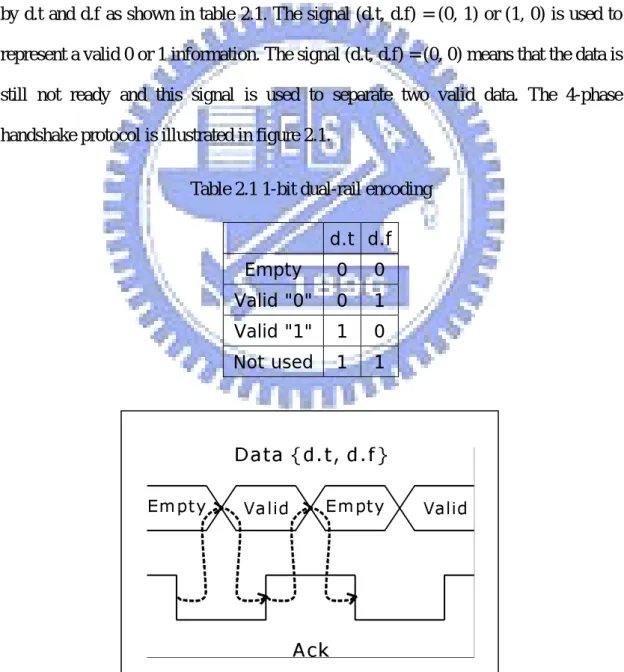
In dual-rail handshake protocols, data signals and timing information are combined by a special encoding mechanism. It can be used to detect whether the signal is ready or not by the encoding signals directly. Therefore this protocol is very robust for delays, and can be applied to variable environments. In the 4-phase dual-rail protocol, two physical wires are needed to encode one-bit information. A data, D, is represented by d.t and d.f as shown in table 2.1. The signal (d.t, d.f) = (0, 1) or (1, 0) is used to represent a valid 0 or 1 information. The signal (d.t, d.f) = (0, 0) means that the data is still not ready and this signal is used to separate two valid data. The 4-phase handshake protocol is illustrated in figure 2.1.
Table 2.1 1-bit dual-rail encoding d.t d.f Empty 0 0 Valid "0" 0 1 Valid "1" 1 0 Not used 1 1
2.2 Delay models
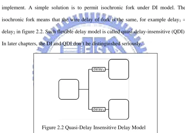
Because data and timing information are combined, the circuits can operate correctly under any gate and wire delay. These circuits are classified as delay-insensitive (DI) circuits. Besides dual-rail, there are still some other encoding techniques, such as 1-of-4. With these coding mechanisms, data and timing information are also combined and the circuits can be delay-insensitive, too.
However, there are too many constraints in pure DI circuits that make it hard to implement. A simple solution is to permit isochronic fork under DI model. The isochronic fork means that the wire delay of fork is the same, for example delay1 =
delay2 in figure 2.2. Such flexible delay model is called quasi-delay-insensitive (QDI).
In later chapters, the DI and QDI don’t be distinguished seriously.
Figure 2.2 Quasi-Delay Insensitive Delay Model
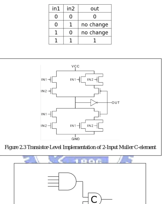
2.3 Muller C-element
The Muller C-element is widely used for asynchronous circuits design. The truth-table of 2-input C-element is shown in table 2.2. The output will change to 1 (or 0) only if both two input are change to 1 (or 0), otherwise the output will hold the previous value. The transistor level implementation of C-element is shown in figure2.3[10]. An alternative costless implementation of C-element is shown in figure2.4, which is used when the number of inputs is large.
Table 2.2 Truth Table of 2-Input Muller C-element
in1 in2 out
0 0 0
0 1 no change
1 0 no change
1 1 1
Figure 2.3 Transistor-Level Implementation of 2-Input Muller C-element
Figure 2.4 Alternative Muller C-element Implementation
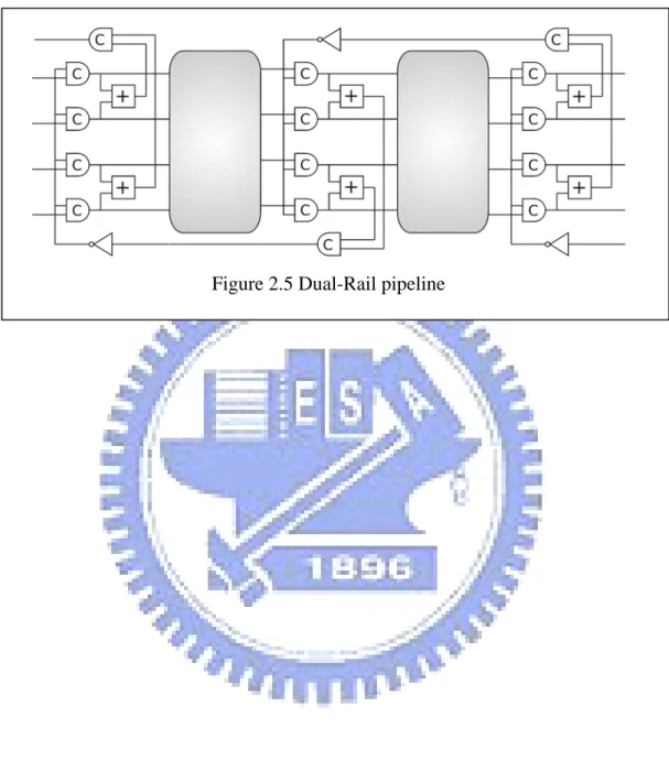
2.4 4-Phase Dual-Rail Pipeline
A 4-phase dual-rail pipeline is based on the Muller Pipeline[11]; however the request signal can be eliminated by the encoding of data. Figure 2.5 shows the three
stage dual-rail pipeline model. Because two valid consecutive data are separated by an empty data in DI circuits, the utilization of the pipeline is only 50%.
Chapter 3: Previous Work
APIC18 is developed by us in NCTU in 2006. The APIC18 is an asynchronous RISC processor which implements most instructions of Microchip’s PIC18. It is based on QDI delay-model and four-phase handshake protocol. It is robust for supply voltage, temperature, and processing parameters.
The instruction set and architecture of Microchip’s PIC18 will be described roughly in this chapter first. Then the design concepts and each function block of APIC18 will be introduced. Most of these features will be used in APIC18S. Finally, the bottleneck of performance will be discussed in section 3.2.7.
3.1 Introduction of Microchip’s PIC18 Microcontroller
The APIC18 is an asynchronous implementation of Microchip’s PIC18 microcontroller. The PIC18 is an 8-bit RISC microcontroller based on the Harvard architecture. It has the separated instruction memory (up to 2MB) and data memory (up to 4MB). The instruction is 16-bit wide, and the data is 8-bit wide. There are 77 instructions provided. Besides, there is a multiplier in PIC18 that makes the multiply execution in a single instruction cycle.
3.1.1 Data Memory Map
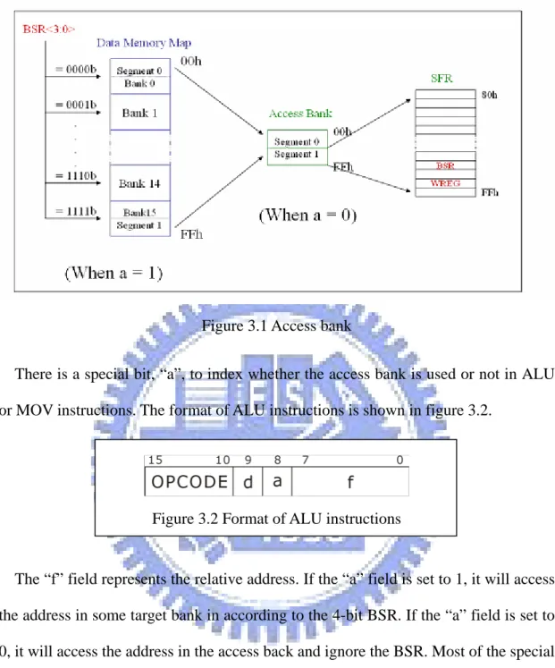
The data memory is 4MB, and each data is 8 bits. That is to say, it needs 12 bits address to access such memory. In PIC18, it has 16 banks of 256 bytes data memory. Corresponsively, a 4-bit base address from BSR and an 8-bit relative offset to generate the 12-bit physical address, as shown in figure 3.1. It should be noted that, a segment of bank0 and a segment of bank15 comprise the “access bank”.
Figure 3.1 Access bank
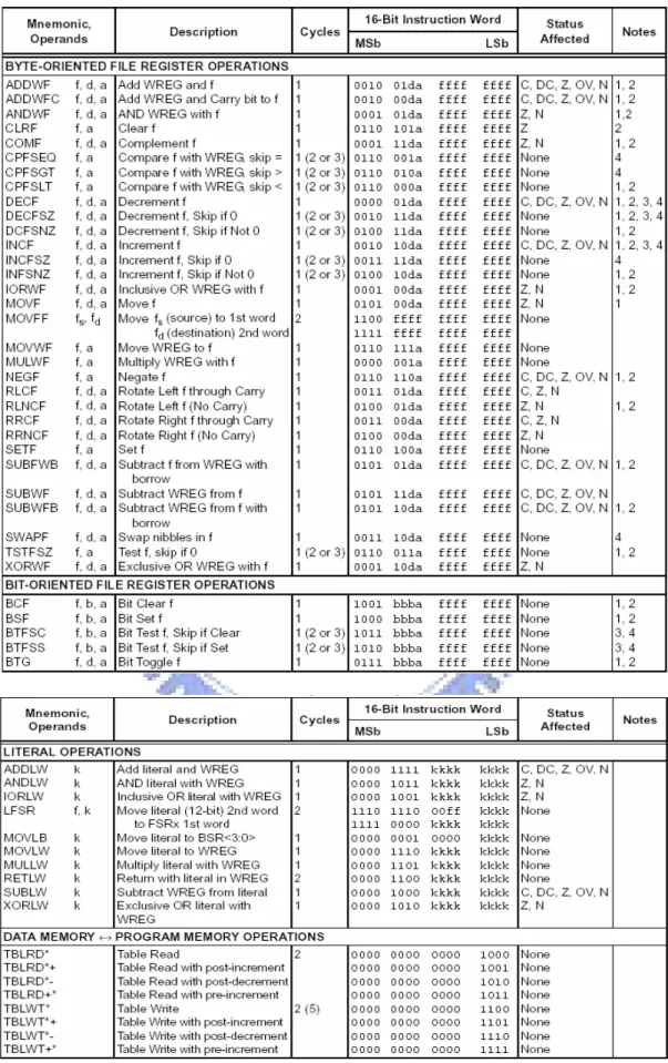
There is a special bit, “a”, to index whether the access bank is used or not in ALU or MOV instructions. The format of ALU instructions is shown in figure 3.2.
Figure 3.2 Format of ALU instructions
The “f” field represents the relative address. If the “a” field is set to 1, it will access the address in some target bank in according to the 4-bit BSR. If the “a” field is set to 0, it will access the address in the access back and ignore the BSR. Most of the special function registers, including BSR, are in the access bank. If the target bank needs to be changed, the BSR in access bank should be modified first.
3.1.2 Instruction Set
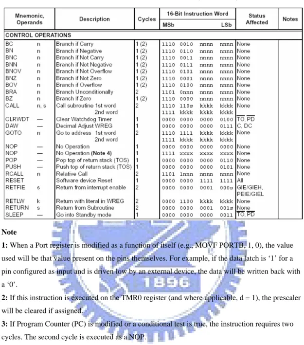
There are 77 instructions available in PIC18 series. Each instruction is a 16-bit word that divided into an opcode and one or more operands.
The instruction set is highly orthogonal and grouped into four basic categories: • Byte-oriented operations
• Bit-oriented operations • Literal operations • Control operations
Most byte-oriented instructions have three operands: 1. The file register (specified by ‘f’)
2. The destination of the result (specified by ‘d’) 3. The accessed memory (specified by ‘a’)
The file register designator ‘f’ specifies which file register is to be used by the instruction. The destination designator ‘d’ specifies where the result of the operation is to be placed. If ‘d’ is zero, the result is placed in the WREG register. If ‘d’ is one, the result is placed in the file register specified in the instruction.
All bit-oriented instructions have three operands: 1. The file register (specified by ‘f’)
2. The bit in the file register (specified by ‘b’) 3. The accessed memory (specified by ‘a’)
The bit field designator ‘b’ selects the number of the bit affected by the operation, while the file register designator ‘f’ represents the number of the file
The literal instructions may use some of the following operands: • A literal value to be loaded into a file register (specified by ‘k’)
• The desired FSR register to load the literal value into (specified by ‘f’) The control instructions may use some of the following operands:
• A program memory address (specified by ‘n’)
Table 3.1: The PIC18 Instruction Set (Continued)
Note
1: When a Port register is modified as a function of itself (e.g., MOVF PORTB, 1, 0), the value
used will be that value present on the pins themselves. For example, if the data latch is ‘1’ for a pin configured as input and is driven low by an external device, the data will be written back with a ‘0’.
2: If this instruction is executed on the TMR0 register (and where applicable, d = 1), the prescaler
will be cleared if assigned.
3: If Program Counter (PC) is modified or a conditional test is true, the instruction requires two
cycles. The second cycle is executed as a NOP.
4: Some instructions are 2-word instructions. The second word of these instructions will be
executed as a NOP unless the first word of the instruction retrieves the information embedded in these 16 bits. This ensures that all program memory locations have a valid instruction.
3.2 Asynchronous PIC18 Implementation – APIC18
APIC18 is a 4-stage pipelined processor based on the 4-phase dual-rail handshake protocol and QDI delay model. In this section, each block of APIC18, including pipeline stages, registers, memory interface, and bypass circuits etc. will be described in detail. The drawback will also be discussed before introducing the new implementation, the APIC18S.
3.2.1 Construct the Basic Elements
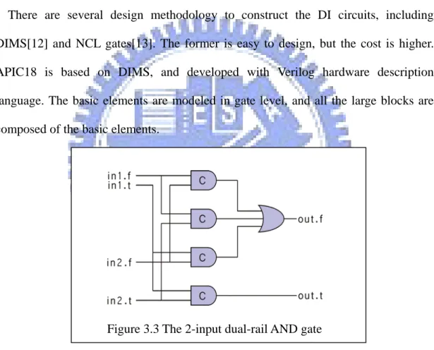
There are several design methodology to construct the DI circuits, including DIMS[12] and NCL gates[13]. The former is easy to design, but the cost is higher. APIC18 is based on DIMS, and developed with Verilog hardware description language. The basic elements are modeled in gate level, and all the large blocks are composed of the basic elements.
Figure 3.3 The 2-input dual-rail AND gate
Figure 3.3 shows the 2-input dual-rail AND gate. Only when both inputs are valid data, the output becomes valid data; only when both inputs are NULL, the output becomes NULL. By using the same concepts, other dual-rail basic elements are constructed, including OR, XOR etc. These basic elements are used to construct the half adder, full adder, 8-bit ripple adder, and ALU block in hierarchical.
3.2.2 Pipeline Architecture
The block diagram of APIC18 is shown in figure 3.4.
Figure3.4 4-stage pipeline architecture
Instructions are executed through 4 stages, namely, IF (Instruction Fetch), ID (Instruction Decode), OF (Operand Fetch), and EXE/WB (Execution & Write Back).
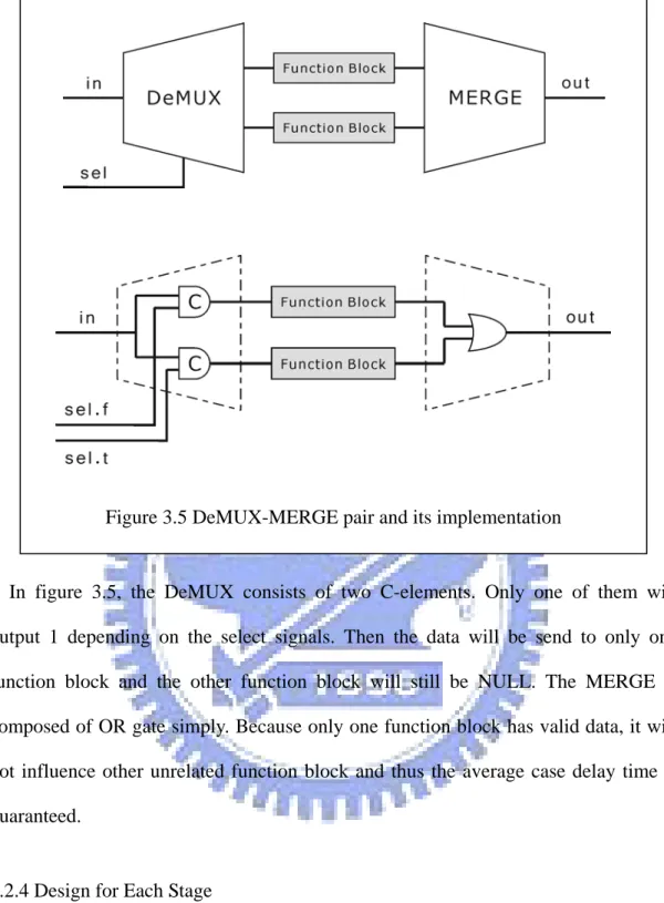
3.2.3 DeMUX and MERGE
In synchronous processor design, data path may have several different works depending on the instruction type. Because the clock period is restricted in worst case delay, designers usually do all the works in parallel and simply use a multiplexer to select one result to output. But in DI circuits, the data and timing signals are combined and it is possible to determine the accurate delay time. It’s possible to design circuits that can operate in different length of time and no longer to let data flow through all function blocks. For this reason, the DeMUX-MERGE pair is proposed to control the data flow. The 1-bit-select DeMUX-MERGE pair is shown in
Figure 3.5 DeMUX-MERGE pair and its implementation
In figure 3.5, the DeMUX consists of two C-elements. Only one of them will output 1 depending on the select signals. Then the data will be send to only one function block and the other function block will still be NULL. The MERGE is composed of OR gate simply. Because only one function block has valid data, it will not influence other unrelated function block and thus the average case delay time is guaranteed.
3.2.4 Design for Each Stage
As introduced in section 3.2.2, APIC18 has four pipelined stages. They are described more detailed as follows.
IF stage:
In the IF stage, the “Read” signal controls the output for valid data or null data. When the Read signal is high, it reads PC value from the PC register and then retrieves the instruction from the program ROM. In addition, the current PC value is
sent to ID stage for calculating the next PC value.
ID stage:
In order to deal with conditional branch instructions simply, the conditional branch instructions are treated as two instruction cycle instructions. The conditional branch instructions are handled in the ID stage. The ID stage mainly consists of four parts, which are described in the following.
Instruction Decode: The Instruction Decode block decodes the input instructions
and generates the control signals to the whole processor. It also requests NPC to generate next PC value directly if the input instruction is not a conditional branch.
Branch Control: If the current input instruction is a conditional branch instruction,
the Instruction Decode requests the Branch Control to deal with it. The Branch
Control reads the value in the STATUS register to decide whether the branch is a
taken or non-taken branch and then request the NPC to generate corresponding next PC value.
Stall Control: If the instruction is a conditional branch instruction and it is executed
the first time, the Stall Control will request the NPC to generate the same PC value again in order to retrieve this instruction again. The mechanism can guarantee that the STATUS register can be correctly updated by the EX/WB stage.
NPC Control: The NPC Control is responsible to generate the correct next PC
value corresponding to the input control signals.
OF Stage:
The OF stage is responsible to prepare source data and destination information for the EXE/WB stage. The address mapping is also done in this stage.
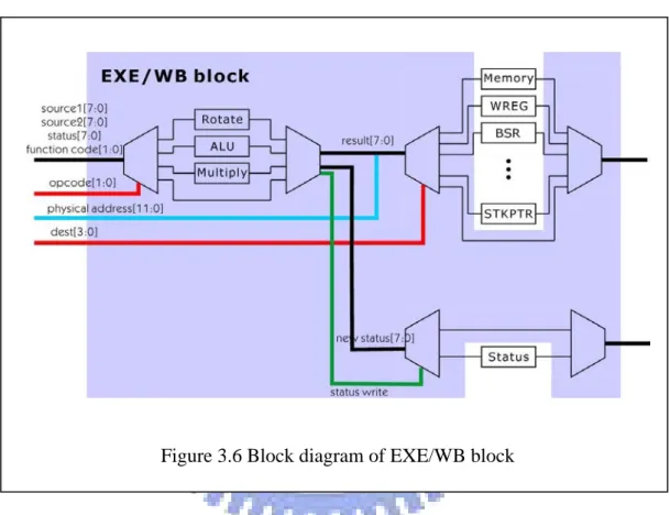
EXE/WB Stage:
from the OF stage. Figure 3.6 is the block diagram of EXE/WB Stage. The DeMUX-MERGE pairs described in section 3.2.3 are widely used to control the data flow to accomplish the average case delay. Besides the top of the stage, we also implemented this model on the all sub-stages of EXE/WB stage. With this model, the EXE/WB stage may exploit data-dependent operations easily. Some operations of each of all the three sub-stages may even be directly bypassed without waste of time.
Figure 3.6 Block diagram of EXE/WB block
3.2.5 Registers
The registers of APIC18 is similar to TITAC’s ones. Figure 3.7 shows a 1-bit dual-rail registers
Figure 3.7 Register
The two NOR gates comprise a latch and is used to hold the value of data. The acknowledgement is set to 1 only when input signals have been saved in the latch. This can be guaranteed by comparing the inputs and outputs of the latch. In APIC18, the registers can be combined with DeMUX-MERGE pairs to make the operation more effective. If the current instruction doesn’t need to write the result to the register, the valid data doesn’t send to the register and the acknowledgement will be NULL. To read the data from the register, the “read” signal is set to 1 and the dout.f and dout.t will be sent back. Finally, it should be pointed out that because the DeMUX-MERGE pairs are only applied to the EXE/WB stage in APIC18 but not to OF stage, it needs an extra OR gate to produce the data0 back to the OF stage that makes the instruction continue to be executed.
3.2.6 Memory Interface
single-rail to dual-rail, and vice verse. Figure 3.8 shows the adapter between instruction memory and the IF stage.
Figure 3.8 Memory interface
3.2.7 Data Hazards and Control Hazard
In order to avoid data hazard, the execution and write back part are combined in EXE/WB stage and adjacent to OF stage. The data memory and WREG register cannot be read and written at the same time, and thus the data hazard never happens.
The control hazard of PIC18 is similar to data hazard because whether the branch is taken or not depends on the status register that is set in the previous instruction. Therefore it must guarantee that the branch instruction must be executed after the
result of previous instruction has been written. Because the branch instruction is handled in the ID stage and status is written in the EXE/WB stage in APIC18, they may be porcessed at the same time. Thus, it may cause some trouble on branch instruction handling in ID stage. In order to simplify the branch instruction handling, if the current instruction is a branch instruction and it is executed the first time, the next program counter will be set to current program counter and this branch instruction is changed to NOP instruction. Then the branch instruction will be retrieved again and the status has been completely written back at this time.
To deal with control and data hazard with this mechanism is simple and it only needs an extra “stall” flag and the cost is very small. However, it may cause serious performance degradation. A new implementation will be proposed in the next chapter.
Chapter 4: A High-Performance
Implementation – APIC18S
Based on our pervious design introduced in chapter 3, some new approaches are proposed in APIC18S to improve the performance observably.
A new stall policy is added into the new implementation, APIC18S, and thus the branch instruction can be handled more effectively. An acknowledge wire is added between the ID and WB stage. If the previous instruction has been finished in the WB stage, the acknowledgement signal will be generated. When a control hazard has been detected, the branch instruction will be stalled at the ID stage until the acknowledgement signal has been pulled up to inform that the previous instruction has been finished. It no longer needs to fetch the instruction twice from memory, and the performance and power consumption can both be improved.
By use of the stall policy, not only branch hazard but the data hazard can be solved easily. The dependent instruction stalls in the ID stage, and simply waits for the previous instruction finished. Because of solving data hazard problem with stall mechanism, the EXE/WB stage doesn’t need to be merged into one stage at all. They can be divided into two separate pipeline stages (EXE stage and WB stage). In other words, the memory (or WREG register) can be read and written at the same time if there is no data dependency among consecutive instructions. It improves the performance by increasing the parallelism of the pipeline stages.
However, this implementation is no longer a pure delay-insensitive circuit. It needs to add a timing constraint and extra circuits to guarantee the correctness of the pipeline. These overheads will be discussed in sections 4.5 and 4.6.
The new pipeline is shown in figure 4.1.
Figure 4.1 Pipeline in APIC18S
There are 5 stages in APIC18S, including instruction fetch (IF), instruction decode (ID), operand fetch (OF), execution (EXE), and write back (WB). The 10-bit program counter is saved in the PC register. Some 8-bit registers, such as WREG (accumulator), STATUS (flag), BSR (address mapping index), and SKTPTR (stack pointer), etc, can be read and written by these pipeline stages. Because the instruction memory and data memory are both single-rail synchronous memory, it needs an additional circuit to deal with the signal transformations from single-rail to dual-rail, and vice versa. This is done by DMEMAdp and IMEMAdp (the IMEMAdp is in IF stage, and omitted in Figure 4.1).
In the IF stage, it reads the program counter from PC, and sends the address to the instruction memory to retrieve the instruction. During the ID stage, instruction is decoded, and the control signals are generated. The stall controller and branch controller are also located in the ID stage. They are responsible for dealing with data
dependency and control dependency. In the OF stage, the operands are fetched from memory and WREG. These two operands are processed in EXE stage, and the result are written back to memory or WREG in the WB stage.
4.2 Stall Policy
The APIC18S has a special stall policy to handle data dependency and control dependency by stalling the dependent instruction. The stall controller is shown in figure 4.2.
Figure 4.2 Stall controller
In figure 4.2, the control signals (single-rail) are shown as dash-line, and the data signals (dual-rail) are shown as bold-line. Because not every instruction has to be stalled, It needs a DeMUX-MERGE pair (as describe in section 3.2.4) to bypass the non-stall instructions.
When the processor is powered on, the two C-elements are initialized to 0 and the output signal (opCode) is NULL. If a non-stall instruction arrives, the DeMUX sends it to MERGE immediately (bypass circuit) and produces the output. If a dependent instruction arrives and has to wait the completion of previous instruction, the DeMUX
sends it to C-element pair (stall circuit). Because C-elements are initialized to 0 and only one input of C-elements is changed to 1, the output is still 0. After the previous instruction is finished and the acknowledge signal (ack) is set to 1, the C-elements pass the signal. Thus the instruction can be continued to execute.
In the pure DI circuits, the output will stay at NULL until all of the inputs are VALID. That is to say that only one bit needs to be stalled in the stall controller. Thus, this control circuit is very small. In order to identify the instruction easily, we modified the original APIC18 ISA a little. In APIC18S, the branch instructions are identified by inst[15:11], and the ALU instructions are identified by inst[15:12]. Thus, the inst[15] (opCode) can be used to control the stall mechanism. If inst[15] is blocked, the result is never produced even if all other signals are ready.
4.3 ID Stage
ID stage is the second stage of APIC18S. It decodes the instruction and generates the control signals to the OF stage. Additionally, it deals with stall mechanism and branch handling. The block diagram of ID stage is shown in figure 4.3.
The ID block receives the program counter (PC) and instruction (inst) from the IF stage, and it produces control signals to the OF stage. It contains the following major blocks:
Stall controller: As described in section 4.2. It blocks the opCode signal when the instruction has to be stalled. The readSTATUS signal is sent out from the stall controller to deal with control hazards.
Adder: There are two adders in ID stage. They are used to calculate the next program counter.
Branch controller: It deals with branch instructions and sends the next program counter to PC. For a non-branch instruction, it sends next program counter immediately. Otherwise, for a branch instruction, it reads the STATUS register, and decides whether the branch is taken or not.
Control signal generator & address mapping: It generates the control signals and the physical address for data memory. It also accepts signals from stall controller and sends signals to the next stage only if the data hazard has been eliminated.
The adders are independent to the stall controller. It can calculate the next program counter when inputs are ready, even if the instruction is stalled.
4.4 OF Stage
The OF stage is similar to our previous implementation except it has DeMUX-MERGE circuits to bypass some signals. It is shown in figure 4.4.
In APIC18, OF stage has no DeMUX-MERGE pair circuits; thus it reads WREG and data memory for every instruction including branch instructions and NOP instructions. Obviously, its performance is not good. In APIC18S, two
DeMUX-MERGE pairs are added. If the current instruction does not require the source operand, the signals will be bypassed directly.
The “Complement” is used for SUB instruction. It produces a 2’s complement value for source2.
Figure 4.4 OF block
4.5 Registers and Memory feedback problem
In the Muller pipeline, there is no feedback signal between adjacent stages. But in our processor design, the storage elements such as WREG and data memory need some feedback signals. It will make the circuits fault, and must be dealt carefully. In APIC18, the EXE and WB stage are combined in one EXE/WB stage and adjacent to the OF stage. Thus, the data memory and WREG register cannot be read and written at the same time. However, the EXE and WB stage are separated in the new APIC18S core. It is possible to read and write data at the same time.
Figure 4.5 shows the dual-rail pipeline with WREG. In the original Muller pipeline, there is no feedback circuits, data may pass through each stage as fast as possible if
the front stages are not full. If there are two paths from OF to WB, they can flow independently. The shorter path can send data to next stage without waiting the longer path to be finished in the same stage. Based on this mechanism, the performance will be the average case delay, not the worst case delay. For example, if there are two paths P1 and P2, and their delays of each stage are t1OF, t1EXE, t1WB and t2OF, t2EXE, t2WB
respectively, the delay will be
max(t1OF + t1EXE, + t1WB , t2OF + t2EXE, + t2WB), not
max(t1OF,t2OF) + max(t1EXE,t2EXE) + max(t1 WB,t2WB).
Figure 4.5 Dual-rail pipeline with WREG
However, it will become very complex if there are any feedback circuits. In the new APIC18S core, the operand is fetched from WREG in the OF stage and sent to the EXE stage. Then in the EXE stage, the results of the operands are calculated and sent to the WB stage. If a ripple adder is implemented in the EXE stage, because of the propagation delay, the lower bits of result will be generated earlier than the higher bits. Thus, it may cause that the lower bit is written back to the WREG register, even if the higher bits are still in EXE stage. Under this situation, the lower bit in WREG is changed and sent back to OF stage for next instruction execution then to the EXE
stage again. It cause very serious fault.
A simple solution is to give up the average-case delay profit. Thus in the WB stage, the result doesn’t be written back until all of the signals in EXE stage have been completed.
4.6 Timing Constraint
In the pure DI circuits, both wires and gates can have arbitrary delay. However, it must have an extra timing constraint to keep the correctness of the circuits in the APIC18S core. That’s because it needs synchronization between the ID stage and WB stage. There is no global clock and the ID stage and the WB stage are not adjacenct. If a dependent instruction is sent to the ID stage, the previous instruction may have three possible states. It may have been completed; it may totally be incomplete; it may be in execution. If an instruction is stalled and the previous instruction has been completed, the acknowledgement will never be returned. The stalled instruction will always be stalled and the circuits will break down.
A timing constraint must be added to the stall policy. Assuming that the delay time from IF to stall controller is td and the delay time from OF to WB is tp, we must
ensure that td is always smaller than tp.
Although the timing constraint cannot be guaranteed theoretically, it is easy to achieve in practice. That’s because it depends on a relative value, not an absolute value. Furthermore, only the instruction followed by an ALU instruction has to be stalled. Thus, tp includes the data read from data memory, ALU operation and write
back; it isn’t simply the bypass delay time. In fact, in current VLSI technology, td is
Chapter 5: Simulation Result
5.1 Testing Environment
In order to verify the correctness of the design, ModelSim 6.0 is used to verify the correctness of the functionality. Figure 5.1 shows the waveform of the functional simulation. Furthermore, we also tried to synthesize our gate-level deign with Design Compiler. The transistor-level of C-element has been shown in previous chapter. An alternative implementation in gate-level is shown in Figure5.2 and Figure5.3. They are used for synthesis with cell-library, the TSMC .13 process library.
Figrue 5.2 Gate-level implementation of C-element
Figure 5.3 C-element with reset
5.2 Area Report
With TSMC .13 process, the area of basic element is shown in table 5.1. The area of each block of APIC18S is shown in table 5.2.
Table 5.1 The area of basic element
element area(um2
) original OR gate 6.8
C-element 25.5
C-element with reset 27.2 dual-rail OR gate 112
2-way DeMUX-MERGE 109
ripple adder ( 8 bits ) 13008
Table 5.2 The area of each block of APIC18S
area(um2 ) % IF stage 552 0.648 ID stage 43151 50.7 (stall) (169) (0.198) OF stage 4062 4.77 EXE stage 31505 37.0 WB stage 3711 4.36 MEMAdp 630 0.74 Registers 1569 1.84 (WREG) (480) (0.564) (STATUS) (480) (0.564) (PC) (609) (0.715) total 85180 100
The DI elements consist of lots of C-elements and are much larger than single-rail ones. So the area of non-DI part, such as “MEMAdp” and “Registers”, is smaller. The ID stage consists of decoder circuits, stall controller, branch controller and two adders for next-program-counter, and its area is the largest of overall design. Besides, it is noticed that the area of stall controller is very small and only 0.198% of whole circuits.
5.2 Timing Report
stage is shown in Table 5.3
Table 5.3 The worst case delay time of each stage Delay time (ps) C-element 131 IF 550 ID 3378 OF 5382 EXE 25497 WB 3086
The memory access time is ignored in Table 5.3. Because the delay time of IF stage is smaller than other stages, we can ensure that the timing problem discussed in section 4.6 will not happen.
Chapter6: Conclusion and Future Work
In this thesis, we proposed a stall policy for dual-rail 4-phase processor and applied it to our pervious asynchronous PIC processor. With this design method, the data hazard and control hazard can be solved more effectively. It no longer fetches branch instruction twice and the memory reads and writes can be done at the same time when there is no data dependency. Therefore the parallelism of pipeline will be increased. We also synthesis the design with TSMC 0.13 process to make sure that it will work correct. It should be noticed that the extra cost is just only 0.198%.
The dependent instruction should be stalled in the ID stage, and wait for finish execution of the previous instruction. In addition, the result is written to registers (WREG and STATUS) or memory in the WB stage. In fact, the register write is faster than memory write. There are two benefits if the register is written in the EXE stage. First, branch instructions that wait for STATUS can be executed quickly. Second, some ALU instructions that wait WREG finished doesn’t need to stall at all, because the OF stage and EXE stage are adjacent. However it will increase the complication of the design and also introduce the higher cost.
We will increase the utilization of our pipeline if we add some latches between two stages. In the original 4-phase dual-rail pipeline, the utilization is only 50% and only the dependence between two adjacent instructions needs to be checked. If the latches are added, we need to check the four adjacent instructions and it will also make the stall circuits hard to design.
Besides that, there are still other interesting topics for research in the future. Although there is a complete-detect policy in DI circuits, in most situations the delay time is still the worst case delay rather than average case delay. For example, we always need to wait for the sum and carry signals of highest bit in an 8-bit ripple
adder to complete, even if the addition is only 4 bits. A simple solution is to add DeMUX-MERGE pairs to the adder. The adder is separated into two parts. If the addition is less than 4 bits, the DeMUX will bypass the higher part of the adder, and then the execution time can be reduced to only half of original one. Moreover, the area of DeMUX-MERGE pair is very small, as shown in table 5.1 and it can be widely used in dual-rail circuits to improve the performance.
The cost of dual-rail circuits is too high to be commercialized. In practice it may mix with bundled data circuits to reduce the cost. Only the critical path is designed with dual-rail to make the timing correct and others are designed with single-rail. With this design methodology, we don’t need to spend lot of time to adjust the matching delay and the area doesn’t become too large. Moreover, the DeMUX-MERGE pairs can be applied to improve the performance, too.
Reference
[1] Jen-Chien Wu, “Decoder design of the asynchronous PIC microcontroller”, National Chiao Tung University, 2006
[2] J. SparsØ and S. Furber, Principles of asynchronous circuit design – a systems prospective, Kluwer Academic Publishers, London, 2001
[3] S. B. Furber, et.al, “AMULET2e: an asynchronous embedded controller,” in Third International Symposium on Advanced Research in Asynchronous Circuits and Systems, April 1997, pp. 290 – 299.
[4] S. B. Furber, et.al,“AMULET2e:An Asynchronous Embedded Controller,” Proceedings of the IEEE Vol. 87, Issue 2, Feb. 1999, pp. 243 – 256.
[5] S. B. Furber, et.al, “AMULET3: a 100 MIPS Asynchronous Embedded Processor”, in Proceedings of the International Conference on Computer Design, 2000, pp. 329-334.
[6] T. Nanya, et.al, “TITAC: Design of a Quasi-Delay-Insensitive Microprocessor”, IEEE Design & Test of Computer, Summer 1994, pp. 50-63
[7] A. Takamura, et.al, “TITAC-2: A 32-bit Asynchronous Microprocessor based on Scalable-Delay-Insensitive Model,” in Proceedings of the International Conference on Computer Design, Oct. 1997, pp. 288-294.
[8] A J. Martin, et.al, “The Design of an Asynchronous MIPS R3000 Microprocessor,” Proceedings of the 17th Conference on Advanced Research in VLSI (ARVLSI '97), September 15-16, 1997, p.164,
[9] A. J. Martin, et.al, “The Lutonium: a sub-nanojoule asynchronous 8051 microcontroller,” in Proceedings of the Ninth International Symposium on Asynchronous Circuits and Systems, May 2003, pp. 14-23.
[10] G. E. Sobelman and K. Fant, “CMOS circuit design of threshold gates with hysteresis,” in Proc. IEEE Symp. Circuits and Systems, vol. 2, 1998, pp. 61-64.
[11] D. Muller and W. Bartky, “A theory of asynchronous circuits,” in Proceedings of an International Symposium on the Theory of Switching, April 1959, pp. 204-243.