Surface band-bending effects on the optical properties of indium gallium
nitride multiple quantum wells
L.-H. Peng,a)C.-W. Shih, and C.-M. Lai
Department of Electrical Engineering and Institute of Electro-Optical Engineering, National Taiwan University, Taipei, Taiwan, Republic of China
C.-C. Chuo and J.-I. Chyi
Department of Electrical Engineering, National Central University, Chung-Li, Taiwan, Republic of China 共Received 10 December 2002; accepted 28 April 2003兲
We report the use of selective wavelength excitation to examine the surface band-bending effects on the optical properties of 3.0-nm-thick indium gallium nitride 共InGaN兲 multiple quantum wells 共MQWs兲. Under a 355-nm excitation, the In0.18Ga0.82N well emission exhibits a linear dependence on the injected carrier density (Ninj) with a coefficient of共i兲 8.5⫻10⫺18meV cm3 for the spectral blueshift and 共ii兲 3⫻10⫺14V cm2 for the change of internal field at a density up to Ninj ⬃1019cm⫺3at 77 K. When excited by a shorter wavelength at 248 nm, the emission from the thin GaN cap layer quenches, but that from the InGaN wells prevails. These observations are attributed to the transportation of photogenerated carriers from the bent GaN surface and redistribution in the InGaN wells. By solving the rate and Poisson equations with a Fermi-level pinning in the band-structure analysis, the emission from the InGaN/GaN MQWs is shown dominant by the recombination between the high-lying subbands and the screening of internal field effects. © 2003
American Institute of Physics. 关DOI: 10.1063/1.1583869兴
From recent developments in the material growth and device processing on aluminum indium gallium nitride 共Al-InGaN兲, this material system has emerged as a promising light source spanning a wide spectral range from ultraviolet to red.1Commercialization of candela-class InGaN quantum-well 共QW兲 blue/green light-emitting diodes,2 and long-lifetime violet and blue laser diodes3 are examples of such exciting achievements. Despite the progress that has been made in active layer design,4 many of its peculiar optical properties still remain a great mystery to be solved.5A pre-vailing theory ascribes the emission mechanism to the local-ized states6from the growth of InGaN layer.7Alternatively, a characteristic internal field distribution, arisen from the dis-continuity of piezoelectricity ( Ppz) and spontaneous polar-ization ( Psp) at the nitride interface,
8
can also respond to the change of oscillator strength in spectral analysis.9
A general assumption is that the recombination is gov-erned by the localized states at low temperature, whereas at high temperature, it is controlled by the extended states. A recent study,10 however, reveals a drastic reduction in the stability of localized exciton due to the large internal field11 and carrier screening effects12 in the InGaN/GaN QW. This makes the treatment of field distribution inside the nitride multiple QWs 共MQWs兲 an important consideration for the optical analysis.13 The discontinuity of Psp and Ppz at the cap/air interface also imposes a disturbance on the boundary condition. The resultant surface charge, which can be as large as 2⫻1013 cm⫺2, constitutes another issue to be re-solved in the band-structure analysis.14
In this letter, we report a series of photoluminescence 共PL兲 experiments by selective wavelength excitation at
vari-ous temperatures to examine the surface band-bending ef-fects on the optical properties of InGaN/GaN MQWs. We find it essential to include a Fermi-level pinning in the GaN cap layer15 to quantify the carrier redistribution effects. Our analysis indicates the emission properties of the 3.0-nm In-GaN MQWs can be attributed to the dominant transitions between the high-lying subbands and the screening of inter-nal field effects.
Samples used in this study were grown by the metalor-ganic chemical vapor deposition technique.16 The sample structures consisted of, in sequence, an undoped 30- or 50-nm GaN cap layer with three pairs of silicon doped 3.0-nm (Lw) InxGa1⫺xN/GaN MQWs at a concentration of 1018 cm⫺3, followed by a 1.5-m-thick GaN buffer layer of ⬃1017-cm⫺3background doping on the共0001兲 plane of sap-phire substrates. The In composition (x⫽0.15 and 0.18兲 in the well and thickness in the GaN barrier (Lb⫽10 and 7 nm兲 were varied to examine the distribution of internal field ef-fect on the optical properties. The selective wavelength ex-citation experiments were performed by using a third-harmonic generation 共355 nm兲 of neodymium: yttrium-aluminum-garnet 共Nd:YAG兲 laser 共New Wave, USA兲 and a 248-nm KrF excimer laser共TuiLaser, Germany兲. The PL sig-nals were collected from the sample surface, dispersed by a grating spectrometer, and detected by a CCD array.
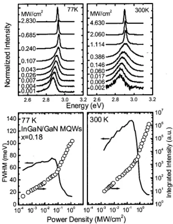
Illustrated in Fig. 1 are the emission spectra measured at 共a兲 77 and 共b兲 300 K from the 3.0-nm In0.18Ga0.82N/GaN MQWs as excited by the 355-nm Nd:YAG laser. Note the peak emission energy remains nearly stationary in the low-density excitation regime (⬍10⫺3 MW/cm2, not shown here, but will be seen in Fig. 4兲 but blueshifts (⬃70 meV) with the increase of pump intensity until a threshold (⬃0.1 and 1 MW/cm2, respectively, for the 77 and 300 K measure-ments兲 is reached. Thereafter, one resumes a spectral redshift a兲Electronic mail: [email protected]
APPLIED PHYSICS LETTERS VOLUME 82, NUMBER 24 16 JUNE 2003
4268
0003-6951/2003/82(24)/4268/3/$20.00 © 2003 American Institute of Physics
(⬃15 meV) with further increase of carrier injection density due to a dominant band-gap renormalization effect.17 The integrated peak emission intensity, as inferred from Fig. 1, exhibits an abrupt change from a linear into square power dependence on the excitation intensity as the latter exceeds the threshold. In concurrence with this, we observe a line-width narrowing, which is followed by a slight broadening due to a contribution from the electron–hole plasma effect.18 The revealing of constant emission peak energy in the low-density excitation (⬍10⫺3MW/cm2) regime, which is independent of the measurement temperature, suggests the state of localization has been minimized in the samples under study. Were this not the case, momentum space filling of the localized or band-tail states by the photogenerated carriers would quickly raise the emission energy. A similar phenom-enon has also been recently reported on the room-temperature emission spectra of a wider 4-nm-thick In0.15Ga0.85N/GaN MQWs.19We further note the temperature dependence of the peak energy shift, as measured in the low-density excitation experiments, reaches only half of the value that would be expected from the Varshni effect. Including the localization effect, however, would enhance rather than com-pensate the energy difference.20 Moreover, referring to the inset of Fig. 2, one notes the emission intensity from the GaN cap layer is two orders of magnitude lower than that from the InGaN wells when excited by a 355-nm laser. By changing the excitation source to a 248-nm laser, we find emission from the GaN cap layer ceases, but that from the InGaN well remains.
To resolve these problems, we adapt a finite difference
method in the band structure analysis21that incorporates so-lutions from the rate and Poisson equations to describe the photo-excitation and carrier redistribution processes at the nitride interface. Since Fermi-level (EF) pinning represents a genuine situation occurred to the undoped n⫺-GaN surface,22 this phenomenon is assessed by a donor-like sur-face state with density ⬃1013cm⫺2 to ensure a pinning of
EFat 0.4 eV below the conduction band edge of n⫺-GaN.23 We let the Roosbroeck–Shockley radiative recombination coefficient of GaN be the only fitting parameter, with a tem-perature dependence following that in Ref. 24. The rest of material parameters are taken as linear interpolations from those in Ref. 25, and a bowing factor of 2.05 eV is used for calculating the band-gap energy of InGaN.
The band-edge profiles shown in Fig. 2 correspond to the boundary condition of 共a兲 periodical field distribution (Fw) ⬀(Pb⫺Pw)•Lb/(Lw⫹Lb)26with a flat surface, and共b兲 sur-face Fermi-level pinning with polarization-induced charge of ⫺“•(Psp⫹Ppz) at each of the nitride interface, respectively. In thermal equilibrium charge neutrality associated with the lineup of Fermi level in 共b兲 determines the amount of free carrier that could be released from the ionized surface state. A nonzero surface electric field in the GaN cap layer (⫺0.17 MV/cm) reflects one such effect and can facilitate the transportation of photogenerated carriers into the adja-cent InGaN wells.
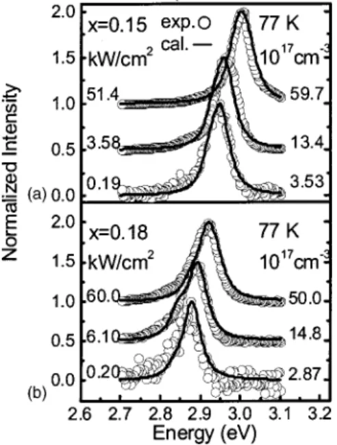
We further note the field strength (⬃2 MV/cm) in the nitride QW, as inferred from the slope of the potential profile shown in Fig. 2, far surpasses that required for the dissocia-tion of localized exciton.27 Under a strong field action, not only can one encounter a reduced oscillator strength, but also a relaxation of parity-selection rule; that is, ⌬n⫽0 among the interband transitions. As a result, one would expect the emission spectra of InGaN MQWs dominated by the 共i兲 high-lying subband transitions whose wave-function overlap in space is less susceptible to the field action and thus leads to larger momentum matrix elements, and 共ii兲 screening of internal field due to the Fermi-level pinning and carrier re-distribution effects. We illustrate in Fig. 3 the normalized emission spectra of 共a兲 x⫽0.15 and 共b兲 x⫽0.18 InxGa1⫺xN/GaN MQWs to elucidate such a principle. The calculation is based upon absorption of photogenerated car-FIG. 1. PL spectra of the 3.0/10.0-nm In0.18Ga0.82N/GaN MQWs excited by
a 355-nm Nd:YAG laser at共a兲 77 and 共b兲 300 K. The spectra have been vertically shifted for comparison.
FIG. 2. Band-edge profiles of the InGaN/GaN MQWs analyzed with and without Fermi-level pinning at the GaN cap layer. Inset: emission spectra of the InGaN MQWs under an excitation of a 248-nm and a 355-nm laser.
4269
Appl. Phys. Lett., Vol. 82, No. 24, 16 June 2003 Penget al.
riers in the thin GaN cap layer and their transportation and redistribution into the InGaN MQWs by substituting a Roosbroeck–Shockley coefficient of 2.73⫻10⫺9 cm3s⫺1 at 77 K and solutions from the rate and Poisson equations to the band structure analysis. Note the agreement with experimen-tal data can extend over three decades of power excitation up to ⬃0.1 MW/cm2 (Ninj⬃1019cm⫺3) and cover a spectral range of 0.2 eV.
Shown in Fig. 4 are data of the measured and calculated peak emission energy of the 3.0 nm 共a兲 x⫽0.15 and 共b兲 x ⫽0.18 InxGa1⫺xN/GaN MQWs, revealing the evolution of spectral blueshift with carrier injection. Further information can be gathered from the inset of Fig. 4, from which one can resolve a linear dependence of the 共i兲 peak energy shift and 共ii兲 decrease in the internal field (Fw) of sample 共b兲 on the carrier injection density (Ninj). The underlying physics is that the originally saw-tooth-like band-edge profile can pro-vide a nonvanishing, first-order correction in the interband transition energy when a perturbation, such as carrier injec-tion, to the internal field occurs. A linear dependence (⬃3 ⫻10⫺14V cm2) of F
w can thus be obtained over two de-cades of density variation in Ninj. Although this coefficient is half of what would be obtained by a simplified slab-like charge model analysis, that is, ␦Fw⬃␦n•Lw/0r, it does reveal the sensitivity of field screening due to the combined effects of surface Fermi-level pinning and carrier redistribu-tion. Such a linear relationship, in turn, translates into a peak energy shift with⬃8.5⫻10⫺18meV cm3 on Ninjdue to the nonzero first-order perturbation on the field screening effect. In summary, we report the use of low-temperature, se-lective wavelength excitation technique to examine the sur-face bending effects on the emission properties of InGaN/ GaN MQWs. The linear dependence of spectral blueshift and emission intensity can be correlated with the decrease of in-ternal field with carrier injection. These observations are as-cribed to the GaN surface Fermi-level pinning and the carrier transportation and redistribution effects in the InGaN wells.
The authors acknowledge S.-M. Fan-Chiang and C.-W. Chang for assistance in the PL measurement. This research was supported by the NSC, Grant Nos. 90-2215-E-002-017 and 023.
1T. Mukai, M. Yamada, and S. Nakamura, Jpn. J. Appl. Phys. 38, 3976 共1999兲.
2S. Nakamura, M. Senoh, N. Iwasa, and S. I. Nagahama, Appl. Phys. Lett.
67, 1868共1995兲.
3
S. Nakamura, M. Senoh, S.-I. Nagahama, N. Iwasa, T. Matsushita, and T. Mukai, Appl. Phys. Lett. 76, 22共2000兲.
4S. Nakamura, Science 281, 956共1998兲.
5F. Ponce and D. Bour, Nature共London兲 386, 351 共1997兲. 6
Y. Narukawa, Y. Kawakami, S. Fujita, and S. Nakammura, Phys. Rev. B
59, 12083共1999兲.
7I.-H. Ho and G. B. Stringfellow, Appl. Phys. Lett. 69, 2701共1996兲. 8F. Bernardini, V. Fiorentini, and D. Vanderbilt, Phys. Rev. B 63, 193201
共2001兲. 9
P. Waltereit, O. Brandt, J. Ringling, and K. H. Ploog, Phys. Rev. B 64, 245305共2001兲.
10M. S. Minsky, S. Watanabe, and N. Yamada, J. Appl. Phys. 91, 5176 共2002兲.
11
G. Traetta, R. Cingolani, A. D. Carlo, F. D. Sala, and P. Lugli, Appl. Phys. Lett. 76, 1042共2000兲.
12S. P. Łepkowski, T. Suski, P. Perlin, V. Yu. Ivanov, M. Godlewski, N.
Grandjean, and J. Massies, J. Appl. Phys. 91, 9622共2002兲.
13J. L. Sa´nchez-Rojas, J. A. Garrido, and E. Mun˜oz, Phys. Rev. B 61, 2773 共2000兲.
14O. Mayrock, H.-J. Wu¨nsche, and F. Henneberger, Phys. Rev. B 62, 16870 共2000兲.
15J. P. Ibbetson, P. T. Fini, K. D. Ness, S. P. DenBaars, J. S. Speck, and U.
K. Mishra, Appl. Phys. Lett. 77, 250共2000兲.
16
C.-C. Chuo, C.-M. Lee, and J.-I. Chyi, Appl. Phys. Lett. 78, 314共2001兲.
17S.-H. Park and S.-L. Chuang, Appl. Phys. Lett. 76, 1981共2000兲. 18S. Bidnyk, T. J. Schmidt, B. D. Little, and J. J. Song, Appl. Phys. Lett. 74,
1共1999兲.
19
E. Kuokstis, J. W. Yang, G. Simin, M. A. Khan, R. Gaska, and M. S. Shur, Appl. Phys. Lett. 80, 977共2002兲.
20P. G. Eliseev, P. Perlin, J. Lee, and M. Osinski, Appl. Phys. Lett. 71, 569 共1997兲.
21
L.-H. Peng, C.-W. Chuang, and L.-H. Lou, Appl. Phys. Lett. 74, 795 共1999兲.
22S. J. Pearton, J. C. Zolper, R. J. Shul, and F. Ren, J. Appl. Phys. 86, 1 共1999兲.
23B. Jogai, J. Appl. Phys. 91, 3721共2002兲. 24
A. Dmitriev and A. Oruzheinikov, J. Appl. Phys. 86, 3241共1999兲.
25L.-H. Peng, Y.-C. Hsu, and C.-W. Chuang, IEEE J. Sel. Top. Quantum
Electron. 5, 756共1999兲.
26V. Fiorentini, F. Bernardini, F. D. Sala, A. D. Carlo, and P. Lugli, Phys.
Rev. B 60, 8849共1999兲.
27
S. Chichibu, T. Azuhata, T. Soda, and S. Nakamura, Appl. Phys. Lett. 69, 4188共1996兲.
FIG. 4. Measured and calculated peak emission energy of the共a兲 x⫽0.15, and共b兲 x⫽0.18 InxGa1⫺xN/GaN MQWs at 77 K. Inset: a linear dependence of the peak energy shift and change of internal field of sample 共b兲 with carrier injection.
FIG. 3. Measured and calculated emission spectra of the 3.0-nm 共a兲 x ⫽0.15, and 共b兲 x⫽0.18 InxGa1⫺xN/GaN MQWs at 77 K. The spectra have been vertically shifted for comparison.
4270 Appl. Phys. Lett., Vol. 82, No. 24, 16 June 2003 Penget al.