Characterization of AC Hot-Carrier Effects in
Poly-Si Thin-Film Transistors
Horng-Chih Lin, Senior Member, IEEE, Kai-Hsiang Chang, and Tiao-Yuan Huang, Fellow, IEEE
Abstract—In this paper, we employed a new test structure
to characterize the alternating-current (ac) hot-carrier (HC)-induced degradation in poly-Si thin-film transistors. High sen-sitivity in detecting the damage and the capability of directly resolving the damage location are demonstrated due to the unique feature of the test structure. Our results indicate that the major degradation is induced in the turn-off stages of the ac-stress signal when applied to the gate and in the turn-on stages of the ac-stress signal when applied to the drain. The availability and energy relaxation of channel HCs are considered to explain the experimental findings.
Index Terms—Alternating-current (ac) stress, hot carriers
(HCs), reliability, thin-film transistors (TFTs). I. INTRODUCTION
P
OLYCRYSTALLINE-SILICON (Poly-Si) thin-film tran-sistors (TFTs) are important building blocks for system-on-panel products [1] and flexible electronics [2]. Owing to the high carrier mobility, the operation speed of poly-Si circuits greatly surpasses that of amorphous-silicon counterparts. Nev-ertheless, this also raises the concern about the generation of hot carriers (HCs) during circuit operation [3]. These energetic carriers may lead to the occurrence of damage events inside the device and degrade the device performance. Evaluations of HC effects are thus important to understand the degradation mech-anisms and to ensure good reliability for practical applications. Since the damage associated with the HC effect is nonuni-form along the channel of the transistor, it is desirable to resolve and understand the detailed mechanisms responsible at different portions of the stressed channel. In our previous works [4], [5], we employed a new test structure, as shown in Fig. 1, to study the characteristics of poly-Si devices under static HC stress tests. Our results indicated that the major-damage location can be directly resolved by the structure and that the evolution of HC degradation can be easily observed owing to its high sensitivity. In practical operations, high pulsed voltages are applied to the transistors in peripheral circuits andManuscript received February 18, 2009; revised May 28, 2009. First pub-lished September 29, 2009; current version pubpub-lished October 21, 2009. This work was supported in part by the National Science Council of Taiwan under Contract NSC-96-2221-E-009-212-MY3. The review of this paper was arranged by Editor J. Suehle.
H.-C. Lin is with the Department of Electronics Engineering and the Institute of Electronics, National Chiao Tung University, Hsinchu 300, Taiwan, and also with the National Nano Device Laboratories, Hsinchu 300, Taiwan (e-mail: [email protected]).
K.-H. Chang and T.-Y. Huang are with the Department of Electronics Engineering and Institute of Electronics, National Chiao Tung University, Hsinchu 300, Taiwan.
Color versions of one or more of the figures in this paper are available online at http://ieeexplore.ieee.org.
Digital Object Identifier 10.1109/TED.2009.2030871
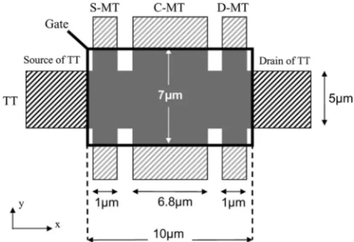
Fig. 1. Top view of the test structure. The slashed regions are n+-doped poly-Si serving as the source or drain of the embedded transistors.
pixel elements [6]. Because the voltage biases are varying with repetitive waveforms during the pulse cycle, HC degradation in such alternating-current (ac) operations behaves differently from that in static operations [6], [7]. In this paper, we study the ac HC effects by taking advantage of the unique feature of the new test structure.
II. DEVICESTRUCTURE ANDAC HC STRESSCONDITIONS
The top view of the test structure is shown in Fig. 1. Details of the device fabrication can be found in our previous reports [4], [5]. In brief, the poly-Si channel was prepared with solid-phase crystallization performed at 600 ◦C in N2 ambient for 24 h. After the definition of the channel regions, an oxide layer was deposited with low-pressure chemical vapor deposition to serve as the gate dielectric. In this paper, the gate oxide thick-ness of the test devices is 30 nm. The test structure actually con-tains several transistors that can be characterized independently. The test transistor along thex-direction, denoted as TT, is de-signed to receive HC stressing. Three monitor transistors (MTs) along they-direction, denoted as S-MT, C-MT, and D-MT, re-spectively, can be characterized independently before and after stressing. With the unique design, damages induced at different portions of the channel can be directly resolved [4], [5].
Two types of stress schemes were employed in this paper. In the first configuration, as shown in Fig. 2(a) and denoted as A-mode stress, the source and drain of TT are applied with 0 V (i.e., grounded) and 15 V, respectively, while a train of voltage pulses with an amplitude of 7.5 V(VG_high) is applied to the gate. The other stress configuration is shown in Fig. 2(b) and denoted as B-mode stress. In this configuration, the source is grounded, the gate is set at 7.5 V, while the drain is applied with
LIN et al.: CHARACTERIZATION OF AC HOT-CARRIER EFFECTS IN Poly-Si THIN-FILM TRANSISTORS 2665
Fig. 2. Configurations of (a) A-mode and (b) B-mode ac stresses. (c) Wave-form of the voltage pulses.Vhighstands forVG_highandVD_highin A- and B-mode stresses, respectively.
a train of voltage pulses with an amplitude of 15 V(VD_high). The waveform of the voltage pulses is shown in Fig. 2(c). The rising time (tr) is defined as the time that the voltage signal rises from 10% to 90% of the amplitude and vice versa for the falling time (tf). For comparison with static HC stress, we define the accumulated stress time as the summation of the durations when the voltage is atVhigh. The duty ratio of the ac signal is defined as the ratio between the time when the voltage isVhigh[thighin Fig. 2(c)] and the cycle time.
III. RESULTS ANDDISCUSSION
A. A-Mode Stress
Fig. 3(a) shows the characteristics of TT before and after receiving A-mode ac stress with a frequency of 500 kHz. For comparisons, the results for static stress underVD= 15 V and
VG= 7.5 V are shown in Fig. 3(b). The total accumulated stress
time is 1000 s for the measurements. In Fig. 3(b), owing to the relatively mild drain and gate voltages used in the stress, the degradation is indeed mild for the device receiving static stress. In the case of ac stress, however, the characteristics are significantly affected. As can be seen in Fig. 3(a), dramatic degradations in subthreshold slope and mobility are observed after ac stress. From the results of density of states (DOS) extracted by the field-effect conductance (FEC) technique [8], [9] (data not shown), we found that the damage mainly comes
from the generation of a large amount of tail states near the conduction-band edge of the poly-Si channel. In Fig. 3(a), we can also see that the deviation inI–V characteristics is larger when measured atVD= 0.1 V, implying that the damage sites are mainly located near the drain side [4]. This implication can be clearly illustrated using the MTs embedded in the test struc-ture. Fig. 4 shows the characteristics of the three MTs contained in the same test sample characterized in Fig. 3(a). Among the three MTs, only the D-MT exhibits dramatic changes after ac HC stress, providing direct evidence of the damage location.
The aforementioned results indicate that additional damage is induced in A-mode ac stress. To further confirm this finding, we also investigated the effect of frequency on degradation, and the results are shown in Fig. 5. Here, the on-current is the drain current of the TT extracted at VG= 10 V and VD= 0.1 V. The degradation of the on-current (in percent) is defined as ΔIon/Ion,0× 100%, where ΔIon= Ion,0− Ion, Ion,0 is the initial on-current and Ion is the on-current after stress. In this figure, it is seen that the current degradation for both TT and D-MT increases monotonically with increasing frequency. In the mean time, the S-MT and C-MT exhibit negligible damage and weak dependence on frequency. It is also worth noting that the D-MT shows higher degradation than the TT, illustrating the enhanced sensitivity of the new test structure.
Fig. 6 shows the degradation in on-current of TT and MTs after stress as a function of duty ratio (thigh/tcycle). In the measurements, the ac-stress time is fixed at 1000 s, which is the summation ofthighaccording to the definition mentioned earlier. The results indicate that the on-current of both TT and D-MT shows a much severe degradation over the case of static stress(duty ratio = 100%). The situation becomes even worse with decreasing duty cycle. Moreover, the D-MT always shows higher degree of degradation as compared with the TT. In contrast, the S-MT and C-MT exhibit negligible degradation and very weak dependence on duty cycle. The trend shown in the figure clearly indicates that the degradation induced in periods other thanVG_highalso contributes to the degradation.
The aforementioned results indicate that additional and ma-jor damages incur during the switching stages, and the damage events are mainly associated with the generation of defects in the channel region near the drain side. The periods when
V = 0 during ac stress are not likely to induce damage in
the device due to the lack of carriers inside the channel. To understand the cause more clearly, we have also investigated the effects of rising and falling times. The results are shown in Fig. 7(a) and (b), where the on-current degradation of TT and D-MT after ac stress is expressed as a function of rising and falling times, respectively. The results indicate that the degradation shows very weak dependence on rising time. In contrast, the degradation worsens significantly when the falling time is reduced.
Based on the aforesaid findings, a scenario for the damage process is proposed. The band diagram shown in Fig. 8(a) corresponds to the situation under static HC stress or ac stress when VG= VG_high. Owing to the high drain voltage, the inversion electrons presenting in the channel are accelerated near the drain side. This leads to the generation of hot electrons and the resultant damage. During the transient period while
Fig. 3. Transfer characteristics of TTs before and after (a) A-mode ac stress with a frequency of 500 kHz and (b) static stress. The accumulated stress time is 1000 s. The rising and falling times of ac stress are both 100 ns.
Fig. 4. Transfer characteristics of the (a) S-MT, (b) C-MT, and (c) D-MT contained in the same test sample characterized in Fig. 3(a) before and after ac stress.
Fig. 5. Degradation of on-current after A-mode ac stress is expressed as a function of frequency. The rising and falling times of ac stress are both 100 ns.
VG is turning off fromVG_highto zero, the inversion electrons remaining in the channel are attracted by the positive drain voltage and will be accelerated toward the drain. Moreover, the
Fig. 6. On-current degradation of the testers after HC stressing as a function of duty ratio.
potential difference between the gate and the drain increases as the gate voltage is reduced, as shown in Fig. 8(b). As a result, the population of “hot electrons” is expected to increase as well.
LIN et al.: CHARACTERIZATION OF AC HOT-CARRIER EFFECTS IN Poly-Si THIN-FILM TRANSISTORS 2667
Fig. 7. Effects of (a) rising time and (b) falling time on the on-current degradation of TT and D-MT after A-mode ac HC stress.
As the falling time shortens, there is less time for the electrons to relax, so excessive HCs would have more impact on the region in the channel near the drain, leading to a higher level of damage. In the present case, the damage is found to be related to the generation of tail states in the poly-Si layer with the effective DOS distribution extracted by the FEC technique [8]. The results are similar to those observed for devices under static HC stress [9]. This indicates that energetic carriers presenting in the channel near the drain tend to create new defects therein by breaking some weak bonds at or near the grain boundaries [10]. On the other hand, there are few free electrons presenting in the channel whenVG is zero, so it is unlikely that a major HC-induced damage will occur at the stage as VG is rising. This explains well the weak dependence on rising time shown in Fig. 7(a).
B. B-Mode Stress
The transfer I–V characteristics of a device before and after B-mode ac stress are shown in Fig. 9. As mentioned in Section II, in this case, a train of pulse voltages withVD_high= 15 V is applied to the drain while the gate voltage is fixed at 7.5 V. The total accumulated stress time is 1000 s, which is identical to that of the A-mode stress performed in Fig. 3(a). It can be seen that, in the present case, a much reduced damage
Fig. 8. Conduction-band(Ec) diagrams under A-mode stress corresponding
to the stages (a) whenVG= VG_highand (b) whenVGis switched off from
VG= VG_high(dashed line). Valence-band level(Ev) in the source is also
shown for reference.
Fig. 9. Transfer characteristics of TTs before and after B-mode ac stress with a frequency of 500 kHz. The accumulated stress time is 1000 s. The rising and falling times of ac stress are both 100 ns.
Fig. 10. Transfer characteristics of the (a) S-MT, (b) C-MT, and (c) D-MT contained in the same test sample characterized in Fig. 9 before and after ac stress.
Fig. 11. Effects of (a) rising time and (b) falling time on the on-current degradation of TT and D-MT after B-mode ac HC stress.
results with B-mode stress. Fig. 10 shows the characteristics of MTs. Still, the major-damage location is near the drain of the TT. However, unlike the situation encountered in A-mode
Fig. 12. Conduction-band diagrams under B-mode stress corresponding to the stages (a) whenVD= 0 and (b) when VD is switched on fromVD= V0
(dashed line). The valence-band level(Ev) at the source is also shown for reference.
stress, the damage is found to be closely related to the rising time rather than the falling time. This is evidenced by the results shown in Fig. 11. In Fig. 11(a), we can see that the degradation in drain current after B-mode stress decreases with increasing rising time. In Fig. 11(b), basically, the damage is found to be independent of the falling time for all three types of MTs.
These observations can be explained with the schemes shown in Fig. 12. Fig. 12(a) shows the band diagram during the stage
LIN et al.: CHARACTERIZATION OF AC HOT-CARRIER EFFECTS IN Poly-Si THIN-FILM TRANSISTORS 2669
when VD is set to zero. The inversion electrons presenting are expected to not cause damage in the channel because the lateral field (i.e., parallel to the channel) is not sufficiently high to accelerate them. During the transient period while VD is switched from low to high level, as shown in Fig. 12(b), the inversion electrons remaining in the channel are attracted by the positive drain voltage and thus tend to be accelerated toward the drain, resulting in additional damages. Moreover, as the rising time is shortened, a faster change in the difference between gate and drain voltages results in the generation of extra hot electrons, so the damage is enhanced.
IV. CONCLUSION
In summary, in this paper, we have employed a new test structure to characterize the ac HC effects. The test structure has been demonstrated to exhibit high sensitivity and the unique capability of directly resolving the damage location. It is also interesting to observe that ac stress would result in additional damage as compared with static stress. In addition, the transient stage that is responsible for the additional damage is identified to be dependent upon the configuration of ac stress. Specifically, our results indicate that the major degradation is induced in the turn-off stages of the ac stress signal when it is applied to the gate, while it is induced in the turn-on stages of the ac stress signal when it is applied to the drain.
REFERENCES
[1] S. Uchikoga, “Low-temperature polycrystalline silicon thin-film transistor technologies for system-on-glass displays,” MRS Bull., vol. 27, pp. 881– 886, Nov. 2002.
[2] M. C. McAlpine, R. S. Friedman, S. Jin, K. H. Lin, W. U. Wang, and C. M. Lieber, “High-performance nanowire electronics and photonics on glass and plastic substrates,” Nano Lett., vol. 3, no. 11, pp. 1531–1535, Nov. 2003.
[3] J. R. Ayres and N. D. Young, “Hot carrier effects in devices and circuits formed from Poly-Si,” Proc. Inst. Elect. Eng.—Circuits Devices Syst., vol. 141, no. 1, pp. 38–441, Feb. 1994.
[4] H.-C. Lin, M.-H. Lee, and K.-H. Chang, “Spatially resolving the hot carrier degradations of poly-Si thin-film transistors using a novel test structure,” IEEE Electron Device Lett., vol. 27, no. 7, pp. 561–563, Jul. 2006.
[5] M. H. Lee, K. H. Chang, and H. C. Lin, “Spatially and temporally re-solving the degradation of n-channel poly-Si thin-film transistors under hot-carrier stressing,” J. Appl. Phys., vol. 101, no. 5, pp. 054518–054522, Mar. 2007.
[6] Y. Uraoka, T. Hatayama, T. Fuyuki, T. Kawamura, and Y. Tsuchihashi, “Reliability of high-frequency operation of low-temperature polysilicon thin film transistors under dynamic stress,” Jpn. J. Appl. Phys., vol. 39, no. 12A, pp. L1 209–L1 212, Dec. 2000.
[7] Y. Toyota, T. Shiba, and M. Ohkura, “A new model for device degra-dation in low-temperature N-channel polycrystalline silicon TFTs under AC stress,” IEEE Trans. Electron Devices, vol. 51, no. 6, pp. 927–933, Jun. 2004.
[8] G. Fortunato and P. Migliorato, “Determination of gap state density in polycrystalline silicon by field-effect conductance,” Appl. Phys. Lett., vol. 49, no. 16, pp. 1025–1027, Oct. 1986.
[9] M. H. Lee, K. H. Chang, and H. C. Lin, “Effective density-of-states dis-tribution of polycrystalline silicon thin-film transistors under hot-carrier degradation,” J. Appl. Phys., vol. 102, no. 5, pp. 054508-1–054508-6, Mar. 2007.
[10] M. Hack, A. G. Lewis, and I. W. Wu, “Physical models for degradation effects in polysilicon thin-film transistors,” IEEE Trans. Electron Devices, vol. 40, no. 5, pp. 890–897, May 1993.
Horng-Chih Lin (S’91–M’95–SM’01) was born in I-lan, Taiwan, on August 1, 1967. He received the B.S. degree from the Department of Physics, Na-tional Central University, Jhongli City, Taiwan, in 1989 and the Ph.D. degree from the Institute of Elec-tronics, National Chiao Tung University (NCTU), Hsinchu, Taiwan, in 1994.
From 1994 to 2004, he was with the National Nano Device Laboratories, Hsinchu, where he was engaged in the research projects of nanoscale device technology development. He joined the faculty of NCTU in 2004, where he is currently a Professor with the Department of Electronics Engineering and the Institute of Electronics. He has authored or coauthored over 200 technical papers in international journals and conferences in the aforementioned areas. His research interests include thin-film-transistor fabrication and characterization, reliability of CMOS devices, and nanowire device technology.
Dr. Lin served on the Program Committee of the International Reliability Physics Symposium (2001 and 2002) and the International Conference on Solid State Devices and Materials (2005–2008).
Kai-Hsiang Chang was born in Tiachung, Taiwan, on November 11, 1981. He received the B.S. degree from the Department of Physics, National Chung Hsing University, Taichung, Taiwan, in 2004 and the M.S. degree from the Institute of Electronics, National Chiao Tung University (NCTU), Hsinchu, Taiwan, in 2008.
He is currently with the Department of Electronics Engineering and the Institute of Electronics, NCTU. His primary research interest is the reliability of poly-Si thin-film transistors.
Tiao-Yuan Huang (F’95) received the B.S.E.E. and M.S.E.E. degrees from National Cheng Kung Uni-versity, Tainan, Taiwan, in 1971 and 1973, respec-tively, and the Ph.D. degree from the University of New Mexico, Albuquerque, in 1981.
After serving for two years in the Taiwanese navy as a fulfillment of his conscription duty, he left for the U.S. in 1977. He had worked in the U.S. semi-conductor industry for 14 years prior to his return to his native country, Taiwan. Since 1995, he has been a Professor with the Department of Electronics Engineering, National Chiao Tung University (NCTU), Hsinchu, Taiwan, where he is also with the Institute of Electronics.
Prof. Huang was a recipient of Semiconductor International’s Technology Achievement Award for his invention and demonstration of the fully overlapped lightly doped drain MOS transistors.