Low-Temperature Activation and Recrystallization of B § and
BF -Implanted LPCVD Amorphous-Si Films
Huang-Chung Cheng, Fang-Shing Wang, Yeong-Fang Huang, and Chun-Yao Huang
Department of Electronics Engineering and Institute of Electronics,
National Chiao Tung University, Hsinchu, Taiwan
Meng-Jin Tsai
United MicroeIectronics Corporation, Science-Based Industrial Park, Hsinchu, Taiwan
A B S T R A C T
L o w - t e m p e r a t u r e (600~ activation a n d recrystallization of the low-pressure chemical v a p o r deposition ( L P C V D ) a m o r p h o u s - S t films B +- a n d B F ~ - i m p l a n t e d with different implantation dosages a n d projection ranges h a v e b e e n investi- gated. T h e b o r o n d o p a n t in the a m o r p h o u s - S t layer can e n h a n c e the recrystallization, resulting in the shorter incubation time a n d smaller grain size then the u n d o p e d specimens. F o r the B F ~ - i m p l a n t e d specimens, the existence of fluorine a t o m s could postpone the grain nucleation, leading to the longer incubation time a n d slower nucleation rate for the heavily d o p e d specimens than the u n d o p e d ones. F o r the B F ~ - i m p l a n t e d specimens, as the implantation p e a k reaches to the ~-SiJSiO2 interface, the recoiled o x y g e n a t o m s f r o m the oxide substrate w o u l d retard the grain nucleation a n d exhibit a significantly large grain size after a long time annealing. H o w e v e r , the recoiled o x y g e n a t o m s a n d the mierodefects in the poly-Si layers w o u l d offset the i m p r o v e m e n t in hole mobility. H i g h e r hole mobilities a n d lower trap state densities w e r e also observed for the B F ~ - i m p l a n t e d specimens with respect to the B+-implanted ones. It is attributed to the passivation effect of fluorine a t o m s within the poly-Si layers.
Introduction
Polycrystalline silicon (poly-Si) deposited b y the low- pressure chemical v a p o r deposition ( L P C V D ) technique is a material of great i m p o r t a n c e in microelectronics technol- ogy. I'2 T h e d o p e d poly-Si film has b e e n e m p l o y e d for a vari- ety of purposes including the intercennection lines be- t w e e n devices, the gate electrode materials for metal oxide semiconductor field effective transistors ( M O S F E T s ) , the resistors or poly-loads for static r a n d o m access m e m o r i e s ( S R A M s ) , the poly-emitter for the bipolar junction transis- tors, 3 a n d the drain/source regions for poly-Si thin film transistors (TFTs), etc. T h e activation of the i m p l a n t e d poly-Si films has b e e n p e r f o r m e d b y using the annealing techniques such as conventional furnace annealing (CFA), 4 rapid thermal annealing (RTA), 5 as well as laser annealing (LA) 6 in high temperature regimes. Recently, in the fabri- cation of three-dimensional (3-D) devices a n d large-area mieroelectrenics, the reduction of the process temperatures for reducing the thermal b u d g e t a n d the d o p a n t redistribu- tion of the underlayer devices b e c o m e s m o r e important. In addition, for the thin-film transistors on glass substrates, the processing temperatures m u s t also m e e t the t e m p e r a - ture tolerance of the substrates. For the a b o v e reasons, the d o p a n t activation at l o w temperature thus needs under- standing.
B o r o n d o p i n g p e r f o r m e d b y B N diffusion source has been used for the p-type d o p a n t in silicon devices. In recent years, ion implantation technique generally replaces tradi- tional furnace diffusion for its precise control of implanta- tion dosage a n d projection range b y properly adjusting the implantation current a n d acceleration voltage. B o t h the B + a n d B F ~ ions are used as the p-type d o p a n t in silicon devices a n d generally activated b y F A or R T A m e t h o d s for the temperature ranging f r o m 700 to ll00~ ~-~ H o w e v e r , the influences of the implantation dosage a n d projection range on the activation a n d grain recrystallization of B + a n d B F ~ - i m p l a n t e d L P C V D a m o r p h o u s - S t (~-Si) films are still u n k n o w n for the lower annealing temperatures. In this paper, l o w temperature activation of B + a n d B F ~ i m p l a n t e d L P C V D ~-Si films with different implantation dosages a n d projection ranges h a v e b e e n studied. T h e B F ~ - i m p l a n t e d specimens exhibit the larger hole mobilities a n d lower acti- vation energies than the B+-implanted ones. Largest grain size can also be obtained for the B F ~ - i m p l a n t e d specimens
as the implantation p e a k reach to the c~-Si/SiQ interface. T h e m e c h a n i s m s for. the d o p a n t activation a n d grain re- crystallization are also p r o p o s e d a n d discussed.
Experimental Procedures
3 in. diameter, (I00) oriented, 4-7 ~l-em, p h o s p h o r u s - d o p e d n-type S f w a f e r s w e r e used in this study. After the initial R C A cleaning, a thermal oxide with 500 n m in thick- ness w a s g r o w n o n the silicon wafers in a s t e a m o x y g e n a m b i e n t to insulate the substrates. U n d o p e d a m o r p h o u s silicon films of i00 n m thickness w e r e then deposited on the oxidized wafers b y using an L P C V D system at 550~ T h e a m o r p h o u s - S t layers w e r e then i m p l a n t e d with B + a n d B~ ions, respectively. Implantation dosages of 4E14, 2E15, a n d I E I 6 i o n / c m ~ with the implantation p e a k to the half thickness of the a m o r p h o u s layer w e r e chosen for the in- spection of dosage effects. To investigate the projection- range effects, implantation depth d o w n to the c~-Si/SiQ interface w a s also p e r f o r m e d with the dosage to be 2 E 1 5 i o n / c m 2. For the B + ions, the corresponding implantation energies to the m i d a n d b o t t o m regions w e r e calculated to be 15 a n d 22 k e V f r o m T R I M simulation. A s for the B F ~ ions, the acceleration voltage of 67 k V w a s a d o p t e d for the half-depth implantation a n d 98 k V for the full-depth case. After the cleaning process, the implanted samples w e r e c a p p e d with a 200 n m p l a s m a - e n h a n c e d chemical v a p o r deposition ( P E C V D ) oxide to prevent the dopants f r o m out- diffusion in the subsequent annealing process. T h e speci- m e n s w e r e annealed in diffusion furnace with N2 a m b i e n t at 600~ for various times. T h e encapsulation oxide w a s then d i p p e d in a diluted H F solution. T h e sheet resistance, effective carrier concentration, a n d hole mobility of the annealed poly-Si films w e r e d e t e r m i n e d b y the four point p r o b e a n d the Hall m e a s u r e m e n t apparatus with v a n der P a u w pattern. T h e crystallinity transformation w a s also inspected b y the x-ray diffraction m e a s u r e m e n t of (iii) silicon peak.~~ Poly-Si resistors with these specimens w e r e also fabricated. T h e d o p a n t profiles of the b o r o n a t o m s w e r e m e a s u r e d b y using a C A M E C A I M S - 4 f secondary ion m a s s spectroscopy (SIMS) with Cs + as the p r i m a r y ion. T h e mierostructure of the poly-Si grains w e r e also observed with transmission electron m i c r o s c o p y ( T E M ) observation. Extraction of the activation energies a n d trap state densi- ties f r o m the t e m p e r a t u r e - d e p e n d e n c e I - V characteristics of the poly-Si resistors w e r e also conducted.
3574 J. Electrochem. Soc., Vet. 142, No. 10, October 1995 9 The Electrochemical Society, Inc.
) unless CC License in place (see abstract).
ecsdl.org/site/terms_use
address. Redistribution subject to ECS terms of use (see
140.113.38.11
<1. Electrochem. Soc.,
Vol. 142, No. 10, October 1995 9 TheElectrochemical Society,
Inc. 3575Results and Discussion
I0<~ Figure l(a) a n d (b) exhibits the S I M S profiles of theboron, oxygen, a n d silicon a t o m s for the 15 a n d 22 k e V i0 ~
B+-implanted specimens with the dosage of 2E15 ion/cm 2,
correspondingly. The higher i m p l a n t a t i o n voltage results i n ~ 1r the deeper i m p l a n t a t i o n depth. The boron tails w i t h i n the = SiOz reveal that boron ions can easily penetrate into the
oxide layer. On the other hand, the SIMS profiles of boron, ~ 1o' fluorine, oxygen, a n d silicon atoms for the BF~-implanted
specimens were shown i n Fig. 2(a) a n d (b). It is found that
the fluorine atoms have the similar distribution like the - ~~ i m p l a n t e d boron atoms. In the inspection of oxygen distri-
bution, a slightly graded oxygen profile near the c~-Si/oxide 10 interface has been observed for the 98 keV i m p l a n t a t i o n
energy with respect to that for the 67 keV one. I n contrast, no significant difference in the oxygen intensity were ob- served between the 15 a n d 22 keV b o r o n - i m p l a n t e d ones. It is a t t r i b u t e d to the higher collision probability of the BF~ ions with SiO~ t h a n that of the B + ones.
After the recrystallization of the i m p l a n t e d specimens, effects of the implantation dosage a n d projection range o n the p h a s e transformation w e r e investigated using the (iii) x-ray diffraction intensities, as s h o w n in Fig. 3. T h e dif- fraction intensities of the u n i m p l a n t e d samples w e r e also
plotted for comparison. Regardless of the i m p l a n t a t i o n 1o '0
dosage a n d energy, all of the B+-implanted specimens dis- play a shorter i n c u b a t i o n time to recrystallize the amor- phous phase t h a n the u n i m p l a n t e d ones, as shown i n Fig. 3. It is reported that the boron dopant can decrease the acti-
i 0 xo l 0 s
7
I 0 ~ .~- 10 4 10 ? 1.0 I q. 0 t l :" B /15keV/2E15cm "z ~ . . . . i . " . S i 2a . A 0.05 , 0.1 0,15 0.2 0 25 0.3 0.35Sputtering Depth (gin) A
0 . 4 I BF +167keV/2E15cm" ~ O" 2 0 I~ D . . . ~ - - ? ' '" ' S .1 s ' "-~( . . . ~ . . . -tr . . . -)( 2-1 . . . . B 11 0.05 0.1 0.15 0.2 0,25 0.3 0.35 0,4
Sputtering Depth (gin) A
BF2
§ 5cm 2 o' ' 1o' [, ... " ' S a s," i 10 6 ~ 10 4 10" 1.0 I . I * i , i . I . I I i , I I 0 0.05 0.1 0.15 0.2 0.25 0.3 0.35 0.4 Sputtering Depth (p.m) BFig. 2. The SIMS profiles of the BF~-implanted specimens with the
implantation energy of (a) 67 and (b) 98 keV, respectively.
vation energy of the epitaxial regrowth a n d enhance the epitaxial regrowth rate3 ~ The faster nucleation rate for the B+-implanted samples is ascribed to the added boron atoms in the ~-Si layers. As for the BF~-implanted specimens, the x - r a y diffraction intensities for the different i m p l a n t a t i o n dosages a n d energies exhibit various time dependence. The medium doped films (the 4E14 ion/cm 2 case) exhibit a faster grain nucleation t h a n the u n i m p l a n t e d ones. How- ever, the longer i n c u b a t i o n times a n d slower transforma-
i0 i~
,o,i
7
" ~ 1 0 ~,I
1 0 4 10 ~ 1.0 B+/22keV/2E15cm': o" - S i ~ S i O , I I /, I i i i i 0.05 0.1 0.15 0.2 0.25 0.3 0.35 0.4 Sputtering Depth (~m) BFig. 1. The SIMS profiles of the B+-implanted specimens with the
implantation energy of (a) 15 and (b) 22 keV, respectively.
250 X-ray Diffraction .*--- _ _ . . - 4 200 / " ,4 / / . 0 ]50 j ' j 3 - / 8B . . . . --m 100 ~ - - - - I - U n i m p l a n t e d ~ -- t - B+ - i m p l a n t e d --ll--1BF~ / 6 7 k e V / 4 E 1 4 c m 4 ~ 50 ~ , : ' ~ : / D , - - - I - B F ~ / 6 7 k e V / 2 E 1 5 c m - ' 9 6 - - o - B F z + / 6 7 k e V / I E l 6cm 4 i' #j~/C3 / / ' - - - * - B F z / 9 g k e V / 2 E 1 5 c m 4 0 ~ I . . . . t . . . . i , , , , I , , , , 5 10 15 20 25 Annealing Time (hr)
Fig. 3. The x-ray intensities of Si(! i 1 ) peak for the different anneal-
ing times.
3576 J. Electrochem. Soc., Vol. 142, No. 10, October 1995 9 The Electrochemical Society, Inc.
Fig. 4. Bright field (BF) micrograph of the undaped amorphous-Si
for 24 h 600~ annealing.
tion rates w e r e attained for the heavily d o p e d specimens (the 2 • i0 TM a n d 1 • 1016 i o n / c m 2 ones). It implies that the
increase of fluorine dose w o u l d postpone the grain nucle- ation. O n the other hand, the deeply i m p l a n t e d case (the 98 k e V one) exhibits the longest incubation time. Moreover, these specimens with slower recrystallization rates will re- sult in higher x-ray intensities d u e to the larger grain size. To u n d e r s t a n d the effects of the implantation dosage a n d energy on the recrystallization of the (~-Si films, these spec- i m e n s annealed for 24 h w e r e also e x a m i n e d with T E M observation. For comparison, the microstructure of the un- d o p e d L P C V D a-St layer w a s also exhibited. T h e dendritic grain structure with average grain size of about 0.2-0.3 txm has b e e n observed for the u n d o p e d specimens, as s h o w n in Fig. 4. T h e microstructure of the s p e c i m e n B+-implanted at 15 k e V to the dosage of 2 E 1 5 i o n / c m 2 w a s also presented in Fig. 5(a). T h e dendritic grains with the average grain size about 0.15-0.2 ~tm w e r e observed. T h e grains for the 4 E 1 4 a n d I E 16 i o n / c m 2 cases also reveal the similar structure but slightly smaller grain size for the higher dose. A s can be seen, all of these B+-implanted samples possess smaller av- erage grain size than the u n d o p e d film. A s for the 22 keV, 2 E 15 i o n / c m 2 sample, it is f o u n d that no m a r k e d difference in the grain microstructure f r o m the 15 keV, 2 E 1 5 i o n / c m 2 one, as s h o w n in Fig. 5(b). It m e a n s that the b o r o n projec- tion range does not significantly influence the grain g r o w t h of the B+-implanted specimens. F o r the solid-phase recrys- tallization, the grain g r o w t h starts at nuclei formation a n d stops w h e n the adjacent grains c o m e into contact with each other. Hence, the lower incubation time a n d the faster nu- cleation rate for the B+-implanted specimens w o u l d cause the smaller grain size than the u n d o p e d ones.
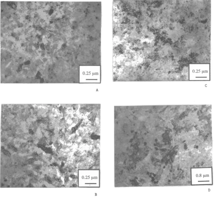
T h e grain structure of the B F ~ - i m p l a n t e d specimens with the implantation dosage ranging f r o m 4 x I0 I~, 2 x 10 ~5, a n d 1 • i016 c m -2 w e r e also s h o w n in Fig. 6(a)-(c), respec- tively. In contrary to the B+-implanted cases, the g r o w n grains reveal the larger grain size for the higher doses a n d a m b i g u o u s grain boundaries for the IE 16"ion/cm 2 case. A s for the specimens i m p l a n t e d at 98 kV, the g r o w n grains reveal the typical grain size of 0.8-1.2 tim in length, as s h o w n in Fig. 6(d). It is significantly larger than those for all the other cases. It also agrees to the x-ray diffraction results, w h i c h s h o w the best crystallinity for the specimens B F ~ - i m p l a n t e d at 98 keV. T h e o x y g e n i m p l a n t e d arnor- p h o u s - S i layers h a v e b e e n reported to possess the high acti- vation energy a n d lower epitaxial g r o w t h rate32 Since the implantation p e a k will reach to the c~-Si/SiO.~ interface for the 98 k e V implantation, it is therefore conjectured that the recoiled o x y g e n a t o m s will incorporate with the p h a s e transformation of the a-St film during the recrystalliza- tion. Therefore, the lower nuclei formation for the deeply B F ~ - i m p l a n t e d specimens is ascribed to the recoiled oxy-
gen a t o m s f r o m the oxide substrate. Similar results w e r e also observed for the deeply Si+-implanted specimens. I~
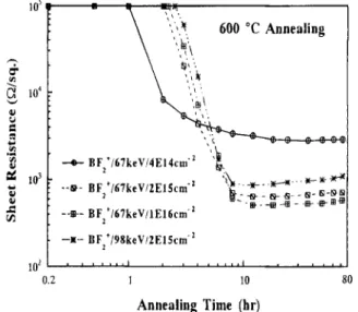
Figure 7 s h o w s the sheet resistances of the B+-implanted samples with the annealing times f r o m 12 m i n to 72 h. It is seen that the sheet resistance decreases dramatically with- in the initial 4 h. After reaching the m i n i m u m value, a slight increase for the further long annealing t i m e s . w a s observed. T h e sheet resistances of the B F ~ - i m p l a n t e d speci- m e n s w e r e also s h o w n in Fig. 8. Different f r o m the B + - i m - planted cases, the sheet resistances still stay at m u c h higher value until the annealing times over i h. It implies that the fluorine a t o m s in the ~-Si layers will postpone the b o r o n activation in the c~-Si layers. In addition, the recoiled o x y g e n a t o m s resulting f r o m the higher implanta- tion energy also lead to longer time delay for the d o p a n t activation.
For a uniformly d o p e d thin film, the sheet resistance (Rs) can be expressed as
l.'.Rs = I I ( N . x q x ~of~ x t) [1] w h e r e q is the electronic charge, Na is the average carrier concentration, ~e~ is the effective carrier mobility, a n d t is the film thickness. A c c o r d i n g to the carrier trapping model, 14 the resistivity (p) a n d the grain b o u n d a r y potential barrier Eb can be expressed as
Fig. 5. BF micrographs of the 600~ annealed B§
speci-
2
mens with dosage of (a) 2E15 ion/cm at 15 keV, and (b) 2E15 ion/
2
cm at 22 keV for 24 h annealing.
) unless CC License in place (see abstract).
ecsdl.org/site/terms_use
address. Redistribution subject to ECS terms of use (see
140.113.38.11
J, Electrochem. Soc,,
Vol. 142, No. 10, October 1995 9 The Electrochemical Society, Inc. 3577Fig. 6. BF micrographs of the 600~ annealed BF~-implanted specimens with dosage of (a) 4E 14 ion/cm 2, (b) 2E 15 ion/cm 2, (c) 1E 16 ion/cm 2
at 67 keV, and (d) 2E15 ion/cm 2 at 98 keV for 24 h annealing.
p = k T • exp ( E J k T ) / ( q 2 • L • N~ • Vc) [2] where k is the B o l t z m a n n constant, T is the measuring tem- perature (in K), L is the grain size, a n d Vc is the collective ve]ocity. As the carrier concentration Na is higher t h a n the trap state density Nt, the potential barrier Eb can be ex- pressed as
Eb = (q2 X N~)/(8 X es, • N~)
[3]
Hence, the trap state density Nt can thus derive f r o m the carrier concentration Na a n d the grain b o u n d a r y potential barrier E~. For convenience, the temperature d e p e n d e n c e of the poly-resistor current expressed as
I = Io • exp ( - E b / k T ) [4] w a s used for the extraction of potential barrier. Then, the trap state density is derived as the Na value is d e t e r m i n e d b y the Hall m e a s u r e m e n t .
T h e sheet resistance (Rs), carrier concentration (N~), hole mobility (F), potential barrier (Eb) , trap state density (Nt) , a n d average grain size (L) for the 24 h annealed specimens are listed in Table I. For the B+-implanted specimens, the carrier concentration increases, but the hole mobility de- creases with increasing implantation dosage. Similar do-
sage d e p e n d e n c e w a s also observed for the B F ~ - i m p l a n t e d samples. It m e a n s that the impurity scattering b e c o m e s the d o m i n a n t factor to influence the carrier transport. T h e trap state density for the B+-implanted samples slightly de- creases with increasing d o p i n g concentration. It implied that the b o r o n d o p a n t could slightly passivate the trap states. A s for the B F ~ - i m p l a n t e d ones, a larger reduction in Nt than the B+-implanted ones w a s observed. It has b e e n reported that the existence of fluorine a t o m s can passivate the poly-Si trap states b y f o r m i n g the Si-F bonds, resulting in the better T F T s characteristics. I~ T h e lower trap state density for the B F ~ - i m p l a n t e d specimens than the B + - i m - planted ones is thus conjectured to the passivation effect of fluorine atoms. O n the other hand, the carrier concentra- tion of the B F ~ - i m p l a n t e d specimens also exhibit a smaller value than the B+-implanted ones w i t h the s a m e implanta- tion dosage. T h e Si-F b o n d formation m i g h t capture s o m e of the activation sites, leading to the lower carrier concen- tration a n d higher sheet resistance than the b o r o n im- planted ones.
A s for the different projection ranges, a lower carrier concentration w a s observed for the deeply i m p l a n t e d ones. It can be realized f r o m the larger b o r o n tails into the oxide substrate for the higher implantation energies, as s h o w n in Fig. 1 a n d 2. F o r the B+-implanted specimens,
3578
J. Electrochem. Soc.,
Vol. 142, No. 10, October 1995 9 The Electrochemical Society, Inc. lO s 104 0 1~ 10 ~ ~k~ 6 0 0 ~ A n n e a l i n g B+/15keV/4E14cm "' "L - - S . - B'/15keV/2El5cm "2 '~ -.~.- B*/15keV/1E16cm "~ -~.- B*/22keV/2E15cm "~ : ~ " ~--s- - d ~ - : ~---~- :~-- -~- -~ ~-~ "~ .-$ _ m- t~-. m. - $- ~-. ~ - fl ~-~ I 0 2 ' , . . . ! , , , , , , , , l . . . 0.2 1 10 80 A n n e a l i n g T i m e (hr)Fig. 7. The sheet resistance of the B+-implanted specimens an-
nealed at 600~ for different annealing times.
lo 5- ",,~. 600 ~ A n n e a l i n g '~ __~ BF2+/67keV/4E14cm'Z "~ ~e 103 ~ . _~_..~.4~... ~-- ~ , ~ .-~-- B F ~ / 6 7 k e V / Z E 1 5 c m "~ ~. - ~ - ~- ~- - ~- ~-~,~ ~ " ~ . . - ~ - 4 ~ - - l i p - ~ - m ~ -'J'- BF ~/67keV/IE16cm 2 --~.- BFz+/98keV/2E15cm2 102 . . . t , , , , , , , , I , . . . 0.2 I 10 80 A n n e a l i n g T i m e (hr)
Fig. 8. The sheet resistance of the BF~-implanted specimens an-
nealed at 600~ for different annealing times.
t h e different i m p l a n t a t i o n energies do n o t e x h i b i t m a r k e d difference in t h e g r a i n s t r u c t u r e a n d e l e c t r i c a l c h a r a c - teristics. As for t h e B F ~ - i m p l a n t e d samples, a s i g n i f i c a n t l y l a r g e g r a i n size w a s o b s e r v e d f o r t h e d e e p l y i m p l a n t e d ones, as s h o w n in Fig. 6(d). It has b e e n e x p l a i n e d above. However, t h e i m p r o v e m e n t in t h e h o l e m o b i l i t y does n o t c h a n g e correspondingly. It m e a n s t h a t n o t only t h e g r a i n size, b u t also t h e r e c o i l e d o x y g e n a t o m s a n d t h e g r a i n m i - c r o d e f e c t s in t h e p o l y - S i layers w o u l d i n f l u e n c e t h e e l e c t r i - cal c h a r a c t e r i s t i c s .
Summary and Conclusions
F o r t h e B + - i m p l a n t e d specimens, t h e b o r o n d o p a n t in t h e L P C V D a - S t l a y e r c a n a c c e l e r a t e t h e g r a i n n u c l e a t i o n , r e - s u l t i n g in a s h o r t e r i n c u b a t i o n t i m e a n d s m a l l e r g r a i n size t h a n t h e u n d o p e d ones. As for t h e B F ~ - i m p l a n t e d samples, t h e f l u o r i n e a t o m s w i l l p o s t p o n e t h e g r a i n n u c l e a t i o n a n d d o p a n t a c t i v a t i o n , r e s u l t i n g in t h e l o n g e r i n c u b a t i o n t i m e a n d s l o w e r g r a i n g r o w t h r a t e for t h e h e a v i l y d o p e d ones. S i g n i f i c a n t l y large g r a i n size has b e e n o b s e r v e d for t h e d e e p l y B F ~ - i m p l a n t e d samples a f t e r a l o n g t i m e annealing. It is c o n j e c t e d t h a t t h e o x y g e n a t o m s r e c o i l e d f r o m t h e o x - ide s u b s t r a t e w i l l cause s l o w e r n u c l e i f o r m a t i o n b u t l a r g e r f i n a l g r a i n size. T h e c a r r i e r c o n c e n t r a t i o n increases b u t t h e h o l e m o b i l i t y decreases w i t h i n c r e a s i n g i m p l a n t a t i o n dosage, r e f l e c t i n g t h a t t h e i m p u r i t y s c a t t e r i n g is t h e d o m i - n a n t f a c t o r i n f l u e n c i n g t h e c a r r i e r t r a n s p o r t . The h i g h e r h o l e m o b i l i t y a n d l o w e r t r a p state d e n s i t y for t h e BF~-im- p l a n t e d s p e c i m e n s w i t h respect to t h e B § ones are a t t r i b u t e d to t h e p a s s i v a t i o n effects of f l u o r i n e a t o m s in t h e p o l y - S i layers.
Acknowledgments
This r e s e a r c h w a s s u p p o r t e d in p a r t by t h e R e p u b l i c of China N a t i o n a l S c i e n c e C o u n c i l (ROC NSC) u n d e r t h e C o n - t r a c t No. N S C - 7 9 - 0 4 0 4 - E 0 0 9 - 0 0 1 . The t e c h n i q u e s u p p o r t s f r o m t h e N a t i o n a l N a n o D e v i c e L a b o r a t o r y of ROC N S C a n d S e m i c o n d u c t o r R e s e a r c h C e n t e r of N a t i o n a l Chiao T u n g U n i v e r s i t y w e r e also a c k n o w l e d g e d . M a n u s c r i p t s u b m i t t e d Oct. 17, 1994; r e v i s e d m a n u s c r i p t r e c e i v e d J u l y 24, 1995.The National Chiao Tung University assisted in meeting
the publication costs of this article.
R E F E R E N C E S
1. T. K a m i n s ,
PolycrystaUine Silicon for Integrated Cir-
cuit Application,
K l u w e r A c a d e m i c Publishers, A m - s t e r d a m (1988).2. S. Wolf a n d R. N. Taauber,
Silicon Processing for the
VLSI Era,
p. 161, L a t t i c e Press, S u n s e t Beach, CA (1986).3. T. H. N i n g a n d R. D. Isaac,
IEEE Trans. Electron
Devices,
E D - 3 2 , 242 (1980).4. E. G. L e e a n d H. B. Im,
This Journal,
138, 3465 (1991). 5. R. A. P o w e l l a n d R. Chow,ibid.,
132, 194 (1985). 6. M. H. J u a n g a n d H. C. Cheng,Appl. Phys. Lett.,
6 0 ,2092 (1992).
7. A. A l m a g g o u s s i , J. Sicart, J. L. Robert, G. Chaussemy, a n d A. Laugier,
J. Appl. Phys.,
6 6 , 4301 (1989). 8. S . R . Wilson, R. B. Gregory, W. M. P a u l s o n , S. J. K r a u s e ,J. D. Gressett, A. H. H a m d i , E D. Mcdaniel, a n d R. G. D o w n i n g ,
This Journal,
132, 922 (1985).9. T. M a k i n o a n d H. N a k a m u r a ,
Solid-State Electron.,
24, 49 (1981).10. K. T-Y. K u n g a n d R. Reif,
J. Appl. Phys.,
59, 2422 (1986).11. L. Cepregi, E. F. Kennedy, T. J. Gallagher, J. W. Mayer, a n d T. W. S i g m o n ,
ibid.,
48, 4234 (1977).12. G. Foti, J. C. Bean, J. M. Poate, a n d C. W. Magee,
Appl.
Phys. Lett.,
36, 840 (1980).13. I.-W. Wu, A. Chiang, M. Fuse, L. Ovecoglu, a n d T. Y. H u a n g ,
J. Appl. Phys.,
65, 4036 (1989).14. G. B a c c a r a n i , B. Ricco, a n d G. S p a d i n i ,
ibid.,
49, 5565 (1978).15. H. N. Chern, C. L. Lee, a n d T. F. Lei,
IEEE Trans. Elec-
tron Devices,
E D - 4 1 , 698 (1994).Table I. The sheet resistance (R,), carrier concentration (No), hole mobility {Ix), potential barrier (Bo),
trap state density {Nt), and average grain size (L) of the specimens annealed for 24 h.
s
~
Rs
(a/[]) B*/15 keV/4E14 cm -2 2783 B§ keV/2E15 cm -2 818 B+/15 keV/1E16 cm -2 437 B§ keV/2E15 cm -2 1000 BF~/67 keV/4E14 cm -2 2860 BFJ67 keV/2E15 cm -2 840 BF~/67 keV/1E16 cm -2 480 BF~/98 keV/2E15 cm -2 1040N. (i/cm 3)
IX (cm2/V. s)
Eb (eV)
Nt (I/cm 2)
Grain size L (ixm)
2.9E19 7.8 0.1 1.23E13 0.15 - 0.2 1.27E20 6.0 0.002 1.16E13 0.15 - 0.2 3.60E20 4.1 0.006 1.07E13 0.1 - 0.15 1.0E20 6.3 0.026 1.17E13 0.15 - 0.2 2.7E19 8.1 0.08 1.07E13 0.15 - 0.2 1.14E20 6.5 0.009 7.35E12 0.2 - 0.3 3.0E20 4.4 0.0026 6.41E12 0.2 - 02 9.1E19 6.7 0.008 6.20E12 0.8 - 1.2
) unless CC License in place (see abstract).
ecsdl.org/site/terms_use
address. Redistribution subject to ECS terms of use (see
140.113.38.11