Nonuniform quantum well infrared photodetectors
S. Y. Wang and C. P. LeeCitation: Journal of Applied Physics 87, 522 (2000); doi: 10.1063/1.371893 View online: http://dx.doi.org/10.1063/1.371893
View Table of Contents: http://scitation.aip.org/content/aip/journal/jap/87/1?ver=pdfcov Published by the AIP Publishing
Articles you may be interested in
Quantum well infrared photodetectors hardiness to the nonideality of the energy band profile J. Appl. Phys. 107, 123110 (2010); 10.1063/1.3446093
Magnetic-field tunable terahertz quantum well infrared photodetector J. Appl. Phys. 98, 084509 (2005); 10.1063/1.2085309
Alloy scattering in GaAs/AlGaAs quantum well infrared photodetector J. Appl. Phys. 88, 288 (2000); 10.1063/1.373655
Current–voltage analysis of a tunneling emitter-undoped single quantum well infrared photodetector J. Appl. Phys. 87, 8575 (2000); 10.1063/1.373581
Noise characteristics of quantum-well infrared photodetectors at low temperatures Appl. Phys. Lett. 76, 206 (2000); 10.1063/1.125703
Nonuniform quantum well infrared photodetectors
S. Y. Wang and C. P. Leea)
Department of Electronic Engineering, National Chiao Tung University, Hsinchu, Taiwan, Republic of China
共Received 29 June 1999; accepted for publication 28 September 1999兲
A nonuniform quantum well infrared photodetector共QWIP兲 structure is proposed. By changing the doping concentration and barrier width of each quantum well, the electric field distribution can be tailored. The nonuniform QWIPs show excellent performance compared with conventional uniform structures. The dark current is about an order of magnitude lower and the background limited temperature increases to 77 K. A detectivity of 2.0⫻1010cm Hz1/2/W and a responsivity of 0.25 A/W at 8.2m have been obtained for these devices. A simple picture of electric field distribution within the structure is described to explain the results. © 2000 American Institute of Physics. 关S0021-8979共00兲07701-X兴
I. INTRODUCTION
In the past decade, a great deal of effort has been put into the development of quantum well infrared photodetec-tors共QWIPs兲.1A large focal plane array with 640⫻468 pix-els has recently been demonstrated.2 The promising perfor-mance made QWIPs a good competitor to traditional HgCdTe detectors. However, despite all the advantages of QWIPs, they usually suffer from high dark current. So one is usually forced to operate the QWIPs below 77 K in order to meet the readout circuit requirement and to achieve the back-ground limited operation.
In a conventional QWIP structure, the same quantum well and barriers are repeated many times. The whole ab-sorption region, which consists of 30–50 identical quantum wells, is generally considered as a uniform active region. The optimization of the QWIP structure is usually concerned with the design of the quantum wells and the barriers but not the structure as a whole. However, some recent studies have revealed that the quantum wells cannot be treated the same.3–5A self-consistent model based on the carrier capture probability and the emission probability has shown that the electric field distribution in the quantum well region is not uniform.4 The electric field in the first few barriers is much higher than that in the rest of the region. The depletion of the first few wells was also found, and it is the cause of the power nonlinearity of the responsivity at high voltages.5So, it becomes clear that the electric field distribution can greatly change the QWIPs’ characteristics.
In this work, we purposely use a nonuniform quantum well structure in a QWIP in order to alter the distribution of the electric field. The doping concentration and the barrier width is not the same for all the quantum wells in the new structure. Lower dark currents and higher gains were ob-tained with the new structure.
II. EXPERIMENTS
Samples used in this work were grown by MBE on a 共100兲 semi-insulating GaAs substrate. For the nonuniform
structure, 35 periods of Al0.27Ga0.73As/GaAs quantum wells were used as the active region. As the growth progressed, the barrier width was increased from 150 to 850 Å, while the doping concentration in the well was decreased from 4 ⫻1018to 5⫻1016cm⫺3. The distributions of the doping con-centration in the wells and the barrier width are shown in Fig. 1. Most of the doping concentration change was made in the first few wells 共from 4⫻1018 to 6⫻1017cm⫺3 for the first eight wells兲 and the barrier width changes linearly but more near the center of the active region. The width of all the quantum wells was kept at 45 Å. The Si dopants in each well were put in the center 25 Å region. The upper and bottom contact layers were 1 m n-type GaAs with a doping con-centration of 2⫻1018cm⫺3. For comparison, a standard sample with a uniform quantum well structure was also pre-pared. The barrier height and the well width were kept the same as the nonuniform structure to ensure the same absorp-tion spectrum. The barrier width and the doping concentra-tion of all the quantum wells were 500 Å and 6 ⫻1017cm⫺3, respectively. The total sheet doping concentra-tion and the barrier width were designed to be the same for both structures, so the absorbance of the samples was kept at the same value. The changes made in the nonuniform struc-ture were to adjust the electric field distribution in the device. After the layers were grown, the absorption spectra were measured by a FTIR using a 45° waveguide configuration. Almost the same absorption characteristics were obtained for both samples. After that, 200m square mesas were defined and formed by chemical etching. Based on the absorption spectrum, which has a peak absorption at 8.4 m, stripe gratings with a 2.8m period were fabricated to couple the normal incident infrared radiation. The gratings were etched into the top contact layer to a depth of 0.7 m. Au/Ge was put on the top and the bottom of the mesas for ohmic con-tacts.
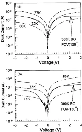
After the devices were fabricated, dark current–voltage (I – V) characteristics at different temperatures and the 300 K background photocurrent at 10 K were measured using a close cycled helium cryostat. In all the measurements, the bottom contact is referenced as ground. As shown in Fig. 2,
a兲Electronic mail: [email protected]
522
0021-8979/2000/87(1)/522/4/$17.00 © 2000 American Institute of Physics
the dark current of the nonuniform QWIP is about an order of magnitude lower than that of the normal structure. But the 300 K background photocurrent is almost the same 共at for-ward bias兲. Because of the lower dark current, the BLIP tem-perature 共with a field of view of 130°兲 of the new nonuni-form QWIP is increased to 77 K, which is significantly higher than that 共72 K兲 measured for the conventional uni-form QWIP prepared side by side.
III. DISCUSSION
To understand why the dark current of the nonuniform QWIPs is lower, we need to know the electric field distribu-tion in the devices. From the concept of current continuity
and by balancing the number of carriers trapped by and the number of carriers escaped from each quantum well, the electric field distribution can be calculated.4 Figure 3共a兲 shows the calculated potential profiles of the nonuniform QWIP under a forward and reverse bias. For comparison, the potential distribution of a uniform structure is shown in Fig. 3共b兲. Because of the nonuniform doping and barrier width, the electric field in the new structure is quite nonuniform. In the highly doped region, the number of free carriers is high so the electric field is low. On the other hand, the lowly doped region has a high electric field.
Both Ref. 3 and 4 have calculated the electric field dis-tribution in conventional QWIPs. Our calculated result on the uniform structure is very similar to that obtained in Ref. 4. In Ref. 3, however, they obtained a field distribution quite nonuniform even in a uniform structure. This is because they used only five wells and a much higher bias field than usual. In our calculation, in order to simulate realistic device opera-tions, we used a realistic device structure under normal bias conditions. The nonuniform electric field can exist even at very small bias voltage for the nonuniform structure.
The effect of nonuniform field distribution on the dark current can be understood in the following way. Suppose the nonuniform structure consists of two regions with different doping concentrations as shown in Fig. 4. The free carrier concentrations 共or the number of carriers that contributes to the dark current兲 in these two regions are n1 and n2 and the
FIG. 1. The distributions of doping concentration and barrier width of each quantum well for the nonuniform sample.
FIG. 2. The dark I – V characteristics at different temperatures and the 300 K background photocurrent for:共a兲 a normal structure and 共b兲 a nonuniform structure.
FIG. 3. The calculated voltage distribution of: 共a兲 a nonuniform sample under positive and negative 1.2 V,共b兲 a uniform sample at 1.2 V.
FIG. 4. The schematic diagram of the two region approximation of the nonuniform sample.
523
J. Appl. Phys., Vol. 87, No. 1, 1 January 2000 S. Y. Wang and C. P. Lee
widths of the two regions are L1 and L2. In the uniform structure, the free carrier concentration is n and the width is
L. n1, n2, and n are obviously proportional to the respective doping concentrations. Since the total sheet doping densities of the two structures are the same, we have
n1L1⫹n2L2⫽nL.
If the total applied voltage is V, we have
V1⫹V2⫽V for L1⫹L2⫽L.
The I – V relationships for the uniform and the nonuniform structures are
I⫽qnV/L
and
I
⬘
⫽qn1V1/L1⫽qn2V2/L2,respectively. Using these relationships, we can easily obtain the ratio between I and I
⬘
, which isI I
⬘
⫽ L1 2 L2⫹ L2 2 L2⫹冉
n1 n2⫹ n2 n1冊
L1L2 L2 . Since n1 n2 ⫹n2 n1 ⭓2, then I I⬘
⭓冉
L1 L ⫹ L2 L冊
2 ⫽1.Therefore, we can see that the dark current of a uniform structure is higher than that of a nonuniform structure if they have the same total sheet carrier density. This is true for both forward and reverse bias conditions. In the simple model presented above, the free carrier concentrations n1and n2are proportional to nW/LB, where nWis the carrier density in the quantum well and LB is the barrier thickness. So, the electric field distribution depends on both nW and LB. However, based on our numerical simulation, the distribution of carrier density in the quantum wells plays a much more important role than the barrier thickness.
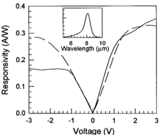
The photoresponse of the devices was measured at 77 K by a Fourier transform IR spectrometer, which was cali-brated by a 1000 K blackbody source. The responsivity spec-trum and the bias dependence of the response are shown in Fig. 5. Similar to the 300 K photocurrent, the bias depen-dence of responsivity is asymmetric. Although the dark cur-rent of this device is much lower, we found that the respon-sivity at forward bias is still very good and is about the same as that of the uniform structure. Normally, the photoresponse is higher for quantum wells with higher doping. In the new structure, the high doping wells are close to the cathode 共in the forward bias case兲. However, as explained above, in this region the electric field is very small. So the electron’s es-cape probability is small and the resulting quantum effi-ciency of these quantum wells also suffers. For the rest of the structure, since the average doping concentration is lower than that of the quantum wells in the uniform structure, the quantum efficiency is lower. Therefore the overall quantum
efficiency of the nonuniform structure should be lower than that of the uniform structure. The reason that we measured very good responsivity for the new structure is due to the increased gain in the device.
We have measured the noise spectral density of the de-vices. From the obtained noise in2and the dark current Id, the gain can be calculated using the following relationship 共as-suming that the G – R noise dominates兲:
gn⫽ in
2 4qId
.
The bias dependence of the noise gain for both samples is shown in Fig. 6. For the nonuniform QWIP, the gain in-creases with bias and saturates at a value of 1.5 at forward bias and 0.55 at reverse bias. For the normal uniform QWIP, the gain saturates at about 0.48. Therefore the new structure has a much higher gain in the forward direction compared to that of the conventional structure.
The increased gain in the nonuniform QWIP can also be understood from the electric field distribution in the device. As shown in Fig. 2, at a forward bias of 1.2 V, the electric field in the first few barriers共near the cathode兲 is nearly zero and then the electric field increases. Near the anode, the elec-tric field becomes very large and is larger than 14 kV/cm.
FIG. 5. The voltage dependence of responsivity of the samples. The solid line represents the responsivity of the nonuniform sample and the dashed line represents the responsivity of the uniform sample. The inset shows the responsivity spectrum of the nonuniform sample.
FIG. 6. The noise gain vs voltage plot for the two samples. The symbols represent the measured results and the lines are the fitting curves.
This strong field can induce impact ionization, which has been observed in n-type quantum wells.6,7 The electrons, which gain enough energy from the field, can interact with the confined electrons inside the quantum well to excite the carriers out of the well. This effect has been found in uni-form QWIPs at large biases.8 Based on theoretical calculations,9the threshold energy to induce impact ioniza-tion is about the same as the activaioniza-tion energy for the carriers in the quantum well and can be even lower if tunneling is taken into consideration. For the quantum well structure that we use, the activation energy is about 130 meV. In the region close to the anode, the barriers are quite thick共see Fig. 2兲. If we take the thickness of those barriers to be 800 Å, the electric field needed to induce ionization is about 16 kV/cm, so the impact ionization happens in this region. Under this situation, we have to re-examine the gain that we found from noise. The noise spectral density with the presence of impact ionization is in 2⫽4qgI d⌬ f
冋
M2冉
2⫺ 1 M冊册
,where M is the multiplication factor and g is the gain without multiplication. If we assume there is no impact ionization for the uniform QWIP 共at least for voltages not too high兲, we can use the g value of the uniform QWIP in the above equa-tion. If we take g to be 0.48, which is the saturated gain of the uniform QWIP, we obtain a multiplication factor of 1.5 at 1.2 V for the nonuniform QWIP using the above equation. For uniform QWIPs, the electric field is much more uniform. Under the same bias voltage of 1.2 V, the electric field is around 8 kV/cm, which is well below the threshold needed for impact ionization. When the nonuniform QWIP is reverse biased, the maximum electric field is also lower than that when it is forward biased. That is why the saturated gain is lower in the reverse direction.
As stated before, the electric field for the nonuniform QWIP under forward bias is nearly zero near the cathode. At such a low field, the electron’s escape probability is around 0.45 for bound to continuum transitions.10 From the doping distribution shown in Fig. 1, the sheet doping density in this low field region is about 6.2⫻1012cm⫺2. The rest of the structure is in the high field region, which has a sheet density of 3.3⫻1012cm⫺2. The escape probability can be assumed to be 1. Since the sheet doping density in the whole structure is 9.5⫻1012cm⫺2 for both the uniform structure and the non-uniform structure, the ratio of the overall quantum efficien-cies for the two devices is
0.45⫻6.2⫻1012⫹3.3⫻1012
9.5⫻1012 ⫽0.64.
Multiplying this number with the multiplication factor of 1.5, we then obtain a responsivity ratio of 0.96. This explains why we obtain a similar responsivity for the nonuniform QWIP 共under forward bias兲 and the uniform QWIP.
So in our new structure, even when the quantum effi-ciency is lower 共than that of the conventional structure兲 un-der forward bias, the responsivity is still good because of a higher gain. At higher biases, the multiplication factor con-tinues to increase and the electron escape probability for higher doping wells also increases, so the responsivity can increase without saturation. This phenomenon can be seen in Fig. 5. We have measured the detectivity of the devices at 77 K. For the new nonuniform QWIP the detectivity is 2.0 ⫻1010cm Hz1/2/W at⫹1 V and maintains the same value to about 2.5 V. But for the normal structure, the detectivity is 1.2⫻1010cm Hz1/2/W at 1 V and decreases to 1.0 ⫻1010cm Hz1/2/W at 1.5 V.
IV. CONCLUSION
In conclusion, a nonuniform QWIP structure is de-scribed. By changing the doping concentration and barrier width of each well, the electric field distribution can be changed. The change in the electric field has a great influ-ence on the detector’s performance. The dark current is about an order of magnitude lower and the gain is significantly higher than those of the conventional uniform structure. The resulting detectivity is also higher and the BLIP temperature is increased to 77 K.
ACKNOWLEDGMENTS
The authors would like to thank Professor C. H. Kuan and M. C. Hsu of National Taiwan University for the noise measurements. This work is supported by the National Sci-ence Council under Contract No. NSC86-2215-E009-010.
1B. F. Levine, J. Appl. Phys. 74, R1共1993兲. 2
S. D. Gunapala, S. V. Bandara, J. K. Liu, W. Hong, M. Sundaram, P. D. Maker, R. E. Muller, C. A. Shott, and R. Carraalejo, IEEE Trans. Electron Devices 45, 1890共1998兲.
3M. Ershov, V. Ryzhii, and C. Hamaguchi, Appl. Phys. Lett. 67, 3147
共1995兲.
4
L. Thibaudeau, P. Bois, and J. Y. Duboz, J. Appl. Phys. 79, 446共1996兲.
5A. Sa’ar, C. Mermelstein, H. Schneider, C. Schoenbein, and M. Walther,
in Intrersubband Transitions in Quantum Wells: Physics and Devices, edited by S. S. Li and Y. K. Su共Kluwer Acadamic, 1998兲, p. 60.
6
F. Capasso, J. Allam, A. Y. Cho, K. Mohammed, R. J. Malik, A. L. Hutchinson, and D. Sivco, Appl. Phys. Lett. 48, 1294共1986兲.
7M. Toivonen, M. Jalonen, A. Salokatve, and M. Pessa, Appl. Phys. Lett.
62, 1664共1993兲.
8B. F. Levine, K. K. Choi, C. G. Bethea, J. Walker, and R. J. Malik, Appl.
Phys. Lett. 51, 934共1987兲.
9S. L. Chuang and K. Hess, J. Appl. Phys. 59, 2885共1986兲.
10B. F. Levine, A. Zussman, S. D. Gunapala, M. T. Asom, J. M. Kuo, and
W. S. Hobson, J. Appl. Phys. 72, 4429共1992兲.
525
J. Appl. Phys., Vol. 87, No. 1, 1 January 2000 S. Y. Wang and C. P. Lee