IEEE ELECTRON DEVICE LETTERS, VOL. 31, NO. 11, NOVEMBER 2010 1233
Novel Symmetric Vertical-Channel Ni-Salicided
Poly-Si Thin-Film Transistors With
High
ON
/
OFF
-Current Ratio
Yi-Hong Wu, Po-Yi Kuo, Member, IEEE, Yi-Hsien Lu, Yi-Hsuan Chen, and
Tien-Sheng Chao, Senior Member, IEEE
Abstract—We have successfully fabricated the symmetric vertical-channel Ni-salicided polycrystalline silicon thin-film tran-sistors (VSA-TFTs) for the first time. The transfer characteristics of VSA-TFTs show a sharp turning between subthreshold and ONstate. TheOFF-state currents can be improved by a modified overetching of oxide, equivalent dual-gate structure, and n+
floating-region length. TheON-state currents can be enhanced by Ni-salicidation. The VSA-TFTs display a good subthreshold swing of 220 mV/dec, steep mobility increase (field-effect mobility of 76 cm2/V· s), and large
ON/OFF-current ratio of more than 109(I
OFF= 4×10⁻¹⁴, ION= 7×10⁻⁵, and Wmask/Lmask=
10 μm/3 μm).
Index Terms—Ni-salicided, polycrystalline silicon thin-film tran-sistors (poly-Si TFTs), symmetric S/D, vertical channel.
I. INTRODUCTION
R
ECENTLY, polycrystalline silicon thin-film transistors (poly-Si TFTs) have attracted considerable attention be-cause of their various commercial applications, such as active-matrix liquid crystal displays, system on panel, nonvolatile memory, and 3-D circuit integration [1]–[4]. However, it is difficult to reduce the device size due to limit of photolitho-graphy resolution. Therefore, vertical-channel thin-film tran-sistors (VTFTs) have been widely developed and studied in many works to overcome the limit of photolithography [5], [6]. In previous works, as the channel lengths are accordingly determined by the thicknesses of poly-Si films instead of the photolithographic limitation, VTFTs show great potentials for 3-D integration. However, their S/D is not symmetric, and the S/D series resistance and contact resistance still remain a problem for device scaling and degrade the device performance. In addition, conventional top-gate poly-Si TFTs suffer from a large OFF-state leakage currents, which are due to a high electric field in the drain depletion region resulting in field emission via grain boundary traps [7], [8]. In order to reduce the leakage currents, many different methods have been proposed to reduce the electric field near the drain region, such as lightly Manuscript received July 2, 2010; accepted July 19, 2010. Date of pub-lication August 30, 2010; date of current version October 22, 2010. This work was supported by the National Science Council, Taiwan, under Contract NSC-97-2221-E-009-152-MY3. The review of this letter was arranged by Editor A. Nathan.The authors are with the Department of Electrophysics, National Chiao Tung University, Hsinchu 300, Taiwan.
Color versions of one or more of the figures in this letter are available online at http://ieeexplore.ieee.org.
Digital Object Identifier 10.1109/LED.2010.2061215
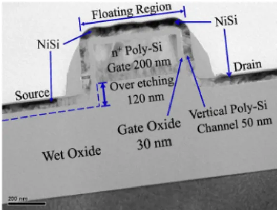
Fig. 1. Cross-sectional TEM microphotograph of the VSA-TFTs.
doped drain, field-induced drain, high-k spacer offset-gated structure, and Si/Ge T-gate structure [9]–[12]. Nevertheless, these structures take additional masks or extra materials (e.g., HfO2, Ge) so that the process will be more complicated. In
this letter, for the first time, the symmetric vertical-channel Ni-salicided polycrystalline silicon thin-film transistors (VSA-TFTs) have been successfully fabricated and demonstrated. The self-aligned silicided S/D, gate, and n+ floating region were formed with Ni, and the offset region was constructed by self-aligned oxide overetching without any additional masks or extra materials. The VSA-TFTs show a sharp turning between subthreshold and ON-state; at the same time, the OFF-state currents can be improved by modifying the oxide overetching depth and n+floating-region length. TheON-state currents can
be enhanced by Ni-salicidation so that the VSA-TFTs display a good subthreshold swing (S.S.), steep mobility increase, and largeON/OFF-current ratio (ION/IOFF) of more than 109.
II. EXPERIMENT
A cross-sectional transmission electron microscope (TEM) microphotograph of the novel VSA-TFTs is shown in Fig. 1. First, bare silicon wafers covered with 550-nm-thick thermal oxide was used as glass substrate. Then, a 200-nm-thick poly-Si thin film was deposited for gate by low-pressure chemical vapor deposition (LPCVD). The gate was implanted with phospho-rous (P+, 70-keV at 5× 1015cm−2) and activated at 600◦C for 12 h in N2 ambient. After gate patterning, the oxide was
overetched to about 120 nm to form the offset region. Then, a 30-nm-thick tetraethoxysilane (TEOS) oxide and a 50-nm-thick undoped amorphous Si (a-Si) were deposited sequentially as 0741-3106/$26.00 © 2010 IEEE
1234 IEEE ELECTRON DEVICE LETTERS, VOL. 31, NO. 11, NOVEMBER 2010
Fig. 2. Schematic cross-sectional view and effective dual-gate structure of the VSA-TFTs.
gate oxide and active region by LPCVD. After the active-region patterning, the a-Si layer was crystallized by solid-phase-crystallization at 600◦C for 24 h in N2ambient.
Then, a 10-nm-thick liner oxide was deposited and 20-keV 5× 1015-cm−2 As+ ion implantations were performed ver-tically to form self-aligned n+ S/D and n+ floating region.
After the As+ ion implantations, a 200-nm-thick TEOS oxide was deposited by LPCVD and etched to form the sidewall spacer. Then, dopants were activated. Next, a stacked 10-nm/ 10-nm TiN/Ni thin film was deposited by sputtering, and Ni-salicidation was carried out at 450 ◦C for 30 s by rapid thermal annealing. The residue Ni was removed by H2SO4:
H2O2 solution. Conventional top-gate horizontal-channel
de-vices with self-aligned n+ S/D and Ni-salicidation were also
fabricated to serve as control ones. Finally, all the devices were fabricated with NH3plasma treatment. We used different NH3
plasma-treatment time (10 min for VSA-TFTs and 30 min for conventional devices) to study the subthreshold characteristics in the exposed poly-Si channels deposited after the gate oxide in the VSA-TFTs and the hidden poly-Si channels under the gate in the conventional devices.
III. RESULTS ANDDISCUSSION
Fig. 2 shows the schematic cross-sectional view and effective dual-gate structure of the VSA-TFTs. The effective channel length (Leff) of the VSA-TFTs with symmetric S/D is defined
by 2× the total thickness of poly-Si gate. The length of the n+floating region is defined by mask channel length (L
mask),
and the mask channel width (Wmask) is equal to the effective
channel width. The offset between the gate and S/D n+edges
was achieved by modifying the wet-oxide overetching. The equivalent dual-gate structure can moderate the lateral electrical field in the drain depletion region, significantly reducing the leakage currents and increasing ION/IOFF[13]. Fig. 3 shows
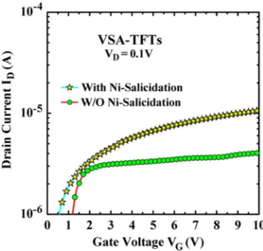
theON-state transfer characteristics of the VSA-TFTs with and without Ni-salicidation. The series resistance of the S/D and the floating n+region can be reduced by Ni-salicidation. Hence, the
ON-state currents can be improved, and they will not be limited with the increase of the gate bias.
Fig. 3. ON-state transfer characteristics of the VSA-TFTs with and without Ni-salicidation.
Fig. 4. Transfer characteristics of the conventional TFTs with W/L = 1 μm/0.35 μm and the VSA-TFTs with Wmask= 1 μm and different Lmask.
The field-effect mobility of the conventional and VSA-TFTs is also shown. Fig. 4 shows the transfer characteristics of conventional TFTs with W/L = 1 μm/0.35 μm and VSA-TFTs with Wmask=
1 μm and different Lmask, and the field-effect mobility of the
conventional TFTs and VSA-TFTs. The VSA-TFTs fabricated with short NH3 plasma-treatment time have higher mobility,
steeper mobility increase, lowerOFF-state currents, better S.S. (∼220 mV/dec.), and approximately equal ON-state currents compared with the conventional TFTs fabricated with long NH3 plasma-treatment time. The improvedOFF-state currents
in the VSA-TFTs are due to oxide-overetching process and equivalent dual-gate structure. The lateral electrical field in the drain depletion region is significantly decreased by S/D n+
offset and equivalent dual-gate structure in VSA-TFTs [13]. The VSA-TFTs with appropriate Lmaskcan moderate theOFF
-state peak lateral electric field in the drain depletion region, and theOFF-state leakage is significantly reduced [14].
Because the floating n+ region was silicided, the series resistance in the floating n+region was effectively diminished, resulting in the maintenance of high ON-state currents with different Lmask. Therefore, ION/IOFF can be enhanced by
increasing the appropriate Lmask(= 3 μm) in the floating n+
region. Moreover, the exposed poly-Si channels deposited after the gate oxide exhibit good interface characteristics resulting
WU et al.: NOVEL SYMMETRIC VSA-TFTS WITH HIGHON/OFF-CURRENT RATIO 1235
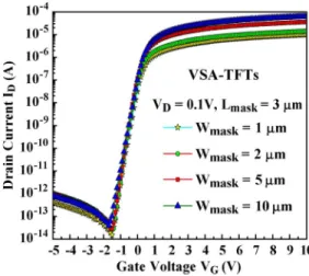
Fig. 5. Transfer characteristics of the VSA-TFTs with Lmask= 3 μm and
different Wmask.
in good S.S. characteristics under short NH3plasma-treatment
time of the VSA-TFTs.
The transfer characteristics of the VSA-TFTs with Lmask=
3 μm and different Wmaskare shown in Fig. 5. TheOFF-state
currents can be suppressed, and the ON-state currents can be enhanced by increasing the Wmask. Hence, ION/IOFFcan be
improved by increasing the Wmask. IONis defined as the drain
current at VG= 10 V and VD= 0.1 V, and IOFFis defined as
the minimum drain current at VD= 0.1 V. The ION/IOFFof
VSA-TFTs with Wmask= 1 μm and 2 μm is about 109, and
the ION/IOFFof VSA-TFTs with Wmask= 5 μm and 10 μm
is more than 109.
IV. CONCLUSION
The novel VSA-TFTs have been presented in this letter. In VSA-TFTs, the poly-Si channels were deposited after the gate oxide and the reversed sequences resulted in good interface characteristics between the gate oxide and poly-Si channels. TheON-state currents can be improved by Ni-salicidation, and theOFF-state currents can be reduced by modifying the oxide overetching, the equivalent dual-gate structure, and the n+ floating-region length without additional mask. The VSA-TFTs have good S.S., high field-effect mobility, and large ION/IOFF
of more than 109.
ACKNOWLEDGMENT
The authors would like to thank the Nano Facility Center of National Chiao Tung University and the National Nano Device Laboratories for providing process equipment.
REFERENCES
[1] S. D. Brotherton, “Polycrystalline silicon thin film transistors,” Semicond.
Sci. Technol., vol. 10, no. 6, pp. 721–738, Jun. 1995.
[2] K. Werner, “The flowering of flat displays,” IEEE Spectr., vol. 34, no. 5, pp. 40–49, May 1997.
[3] T. Y. Chiang, M. W. Ma, Y. H. Wu, P. Y. Kuo, K. T. Wang, C. C. Liao, C. R. Yeh, and T. S. Chao, “MILC-TFT with high- κ dielectrics for one-time-programmable memory application,” IEEE Electron Device Lett., vol. 30, no. 9, pp. 954–956, Sep. 2009.
[4] H. Wang, M. Chan, S. Jagar, Y. Wang, and P. K. Ko, “Submicron super TFTs for 3-D VLSI applications,” IEEE Trans. Electron Devices, vol. 21, no. 9, pp. 439–441, Sep. 2000.
[5] C. S. Lai, C. L. Lee, T. F. Lei, and H. N. Chern, “A novel vertical bottom-gate polysilicon thin film transistor with self-aligned offset,” IEEE
Electron Device Lett., vol. 17, no. 5, pp. 199–201, May 1996.
[6] M. Z. Lee, C. L. Lee, and T. F. Lei, “Novel vertical polysilicon thin-film transistor with excimer–laser annealing,” Jpn. J. Appl. Phys., vol. 42, no. 4B, pp. 2123–2126, Apr. 2003.
[7] J. G. Fossum, A. O. Conde, H. Shichijo, and S. K. Banerjee, “Anomalous leakage current in LPCVD polysilicon MOSFETs,” IEEE Trans. Electron
Devices, vol. ED-32, no. 9, pp. 1878–1884, Sep. 1985.
[8] K. R. Olasupo and M. K. Hatalis, “Leakage current mechanism in sub-micron polysilicon thin-film transistors,” IEEE Trans. Electron Devices, vol. 43, no. 8, pp. 1218–1223, Aug. 1996.
[9] C. T. Liu, C. H. D. Yu, A. Kornblit, and K. H. Lee, “Inverted thin-film transistor with a simple self-aligned lightly doped drain structure,” IEEE
Trans. Electron Devices, vol. 39, no. 12, pp. 2803–2809, Dec. 1992.
[10] K. Tanaka, K. Nakazawa, S. Suyama, and K. Kato, “Characteristics of field-induced-drain (FID) poly-Si TFT’s with highON/OFFcurrent ratio,”
IEEE Trans. Electron Devices, vol. 39, no. 4, pp. 916–920, Apr. 1992.
[11] Z. Xiong, H. Liu, C. Zhu, and J. K. O. Sin, “Characteristics of
high-κ spacer offset-gated polysilicon TFTs,” IEEE Trans. Electron Devices,
vol. 51, no. 8, pp. 1304–1308, Aug. 2004.
[12] P. Y. Kuo, T. S. Chao, P. S. Hsieh, and T. F. Lei, “Characteristics of self-aligned Si/Ge T-gate poly-Si thin-film transistors with highON/OFF
current ratio,” IEEE Trans. Electron Devices, vol. 54, no. 4, pp. 1171– 1176, May 2007.
[13] I. H. Song, S. H. Kang, W. J. Nam, and M. K. Han, “A high-performance multichannel dual-gate poly-Si TFT fabricated by excimer laser irradia-tion on a floating a-Si thin film,” IEEE Electron Device Lett., vol. 24, no. 9, pp. 580–582, Sep. 2003.
[14] Y. C. Wu, T. C. Chang, P. T. Liu, C. W. Chou, Y. C. Wu, C. H. Tu, and C. Y. Chang, “Reduction of leakage current in metal-induced lateral crystallization polysilicon TFTs with dual-gate and multiple nanowire channels,” IEEE Electron Device Lett., vol. 26, no. 9, pp. 646–648, Sep. 2005.