國
國
國
國 立
立
立
立 交
交
交
交 通
通
通
通 大
大
大
大 學
學
學
學
顯示科技研
顯示科技研
顯示科技研
顯示科技研究所
究所
究所碩士班
究所
碩士班
碩士班
碩士班
碩士論文
碩士論文
碩士論文
碩士論文
低溫複晶矽薄膜電晶體背光下之
低溫複晶矽薄膜電晶體背光下之
低溫複晶矽薄膜電晶體背光下之
低溫複晶矽薄膜電晶體背光下之
單位光通量漏電流特性分析
單位光通量漏電流特性分析
單位光通量漏電流特性分析
單位光通量漏電流特性分析
Study on the Mechanism of
Unit-Lux Current Arisen by Back Light
for LTPS TFTs
研
研
研
研 究
究
究
究 生
生
生
生 : 林志融
林志融
林志融 Chih-Jung Lin
林志融
指導教授
指導教授
指導教授
指導教授 : 戴亞翔
戴亞翔
戴亞翔 博士
戴亞翔
博士
博士 Dr. Ya-Hsiang Tai
博士
中華民國 九十九 年 八 月
低溫複晶矽薄膜電晶體背光下之
低溫複晶矽薄膜電晶體背光下之
低溫複晶矽薄膜電晶體背光下之
低溫複晶矽薄膜電晶體背光下之
單位光通量漏電流特性分析
單位光通量漏電流特性分析
單位光通量漏電流特性分析
單位光通量漏電流特性分析
Study on the Mechanism of Unit-Lux Current
Arisen by Back Light for LTPS TFTs
研 究 生 : 林志融 Student : Chih-Jung Lin
指導教授 : 戴亞翔 博士 Advisor : Dr. Ya-Hsiang Tai
國立交通大學
國立交通大學
國立交通大學
國立交通大學
顯示科技研究所
顯示科技研究所
顯示科技研究所
顯示科技研究所碩士班
碩士班
碩士班
碩士班
碩
碩
碩
碩
士
士
士
士
論
論
論
論
文
文
文
文
A Thesis
Submitted to the Display Institute
College of Electrical and Computer Engineering
National Chiao Tung University
in Partial Fulfillment of the Requirements
for the Degree of Master
in
Display Institute
August 2010
Hsinchu, Taiwan, Republic of China
低溫複晶矽薄膜電晶體背光下之
低溫複晶矽薄膜電晶體背光下之
低溫複晶矽薄膜電晶體背光下之
低溫複晶矽薄膜電晶體背光下之
單位光通量漏電流特性分析
單位光通量漏電流特性分析
單位光通量漏電流特性分析
單位光通量漏電流特性分析
學生:林志融 指導教授:戴亞翔 博士
國立交通大學顯示科技研究所碩士班
國立交通大學顯示科技研究所碩士班
國立交通大學顯示科技研究所碩士班
國立交通大學顯示科技研究所碩士班
摘
摘
摘
摘
要
要
要
要
低溫多晶矽薄膜電晶體(LTPS TFTs)已被廣泛研究在平板的應用,例如在主 動式矩陣液晶顯示器(AMLCDs)和主動式矩陣有機發光二極體(AMOLEDs)。高亮 度的背光照明下,光漏電流的存在容易造成畫素電壓的下降而導致串音(Cross talk)的產生。因此,光對低溫薄膜電晶體是值得調查。 在這篇論文中,我們分析了低溫複晶矽薄膜電晶體在背光照明下影響的光漏 電流。我們漏電流在背光下可用一個經驗公式表示。我們也比較了背光和正光條 件下的光行為。定性模型來解釋在熱載子效應(Hot Carrier effect)與自發熱(Self
Heating effect)後產生的缺陷提出相應的光照行為。缺陷中心影響光漏電流的行為
與缺陷陷阱的能級非常相關。在直流偏壓後有兩種缺陷造成。我們提供新的見解 之間的連接缺陷能級和光感應電流,從而進一步確認缺陷的特性。我們相信,這 項研究的背光感應漏電流在設計中考慮是非常有用,並減少漏電流在薄膜電晶體 液晶顯示器中。
Study on the Mechanism of
Unit-Lux Current Arisen by Back Light
for LTPS TFTs
Student:Chih-Jung Lin Advisor:Dr. Ya-Hsiang Tai
Display Institute,
National Chiao Tung University
Abstract
Low temperature polycrystalline silicon (LTPS) thin film transistors (TFTs) have been widely investigated for flat-panel applications, such as for active matrix liquid crystal displays (AMLCDs) and active matrix organic light emitting diodes (AMOLEDs). The high illumination intensity from back light increases the leakage current of LTPS TFTs and results in the decrease of pixel voltage and the increase of cross talk. Therefore, photo effect on LTPS TFTs is worthy of investigation.
In this thesis, we analyze the effect of back light illumination for LTPS TFTs based on the photo leakage current. The leakage current under back light can be expressed by an empirical equation. We also compare the photo behaviors of back light with that of front light condition. Qualitative models are proposed to explain the illumination behaviors corresponding to the defects created after hot carrier stress and self heating stress. Defect center behaviors which influence the photo leakage current are strongly related to the energy level of trap defects. There are two kinds of defects created by DC stress. We provide new insight on the connection between the energy
levels of the defects and the photo induced current, which can further confirm the characteristics of the defects. We believe this study of the backlight induced leakage current can be very useful in the design consideration and the leakage current reduction in the TFT LCD.
Acknowledgements
首先要感謝我的指導教授 戴亞翔博士;感謝老師在這兩年給予我許多的教 導,老師認真做研究的態度和積極的人生觀在這兩年內讓我留下深刻的印象,在 老師出國的這一年,也總是鼓舞我們適時的指導我們,給予我們不同的研究想 法,讓我們用更嚴謹的思考方式去對問題做更進一步的討論。老師也時常告訴我 們許多人生經驗和做事的態度,老師教導的這些經驗累積,讓我在碩士生涯獲益 許多。在此,對老師致上最深的敬意。 此外,還要感謝指導我的彥甫學長,在我研究遇到困難時,不厭其煩的與我 討論,給予我很大的幫助跟建議。感謝畢業的學長姐們,游博、紹文、歐趴、國 珮和耿維不吝的對我伸出援手幫忙,讓我更快的融入這個環境。我更要感謝陪了 我兩年的同學小瓜呆和少宏,在研究的這兩年時常提供知識上的幫助,並對我實 驗上的問題提供解決方法,有你們的幫助讓我的生活也增加了幾分色彩。也要感 謝學弟們:政哲、寬寬、冠銘的幫忙,以及隔壁實驗室的光庭、俊傑、陶莉、敬 儒,碩士兩年的生活有實驗室的所有人陪伴,並且帶來了許多歡笑,讓我的碩士 生活過的更加的充實。 最後,非常感謝我的家人及女友筱薰,在我遇到困難時,總是給我支持和鼓 勵。有我的家人幫助以及你們給我的愛,讓我能無後顧之憂的完成碩士學位,在 此向你們送上我所有的感謝。 志融 2010.08.26Contents
Chinese Abstract
……….………..…………IEnglish Abstract
………..…………..………. IIAcknowledgement
……..………...………...…… IVContents
...………... VTable Captions
………... VIIFigure Captions
……….... VIIIChapter 1 Introduction
1.1 Background ………. 1
1.2 Motivation ………... 1
1.3 Thesis Organization ………. 2
Chapter 2 Characteristics of Photo Leakage Current
2.1 Definition of Unit-Lux Current……
………... 52.2 Experiment Method …………....………... 5
2.3 Behaviors of Unit-Lux Current ..………... 6
2.4 Mechanisms of Unit-Lux Current …..………... 7
2.5 Comparison of Front and Back Light Effects ………... 9
Chapter 3 Effects of the Defects Created by Hot Carrier Stress
3.1 Degradation Mechanism and Stress Condition ……… 223.2 Analysis Unit-Lux Current after Stress ……… 23
3.3 Comparison Front Light with Back Light after Stress .……… 25
Chapter 4 Effects of the Defects Created by Self Heating Stress
4.1 Degradation Mechanism and Stress Condition ……… 344.2 Analysis Unit-Lux Current after Stress …………..……….. 35
Chapter 5 Conclusions
………. 48Table Captions
Chapter 2
Table 2-1 Experiment conditions for VD, VG effects on photo leakage ………12 Table 2-2 The values of fitting factors in equation (2.1) ……….15
Table 2-3 The values of fitting factors in equation (2.4) and (2.5)………..19
Chapter 3
Table 3-1(a) Experiment conditions for hot carriers stress………..28
Table 3-1(b) Measurement conditions for the photo leakage ………..28
Chapter 4
Table 4-1(a) Experiment conditions for self heating stress ……….39 Table 4-1(b)Measurement conditions for the photo leakage …...………39
Figure Captions
Chapter 1
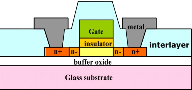
Fig. 1-1 The cross-section views of n-channel LTPS TFTs with LDD structure... 4
Chapter 2
Fig. 2-1 Relationship between leakage current and illumination intensity under Different bias conditions ..………..………..11Fig. 2-2 The cross section of device under back light illumination ……..…………..11
Fig. 2-3 The transmission rate and absorption rate of LED light source.………12
Fig. 2-4 (a) Photo leakage current at Vg= -5V and Vd=0.6V to 15V ……...………..13
Fig. 2-4 (b) Photo leakage current at Vd=5.3V and Vg=-10V to -0.4V ………….…13
Fig. 2-5 (a) Drain bias effect on Unit-Lux Current at different gate biases ………….14
Fig. 2-5 (b) Gate bias effect on Unit-Lux Current at different drain biases ………….14
Fig. 2-6 Second component of Unit-Lux Current (ULCC2) versus drain bias at different gate voltages ………15
Fig. 2-7 Experiment data (symbols) and empirical formula (solid lines) ……….16
Fig. 2-8 (a) Proposed model of ULCC1 mechanism for LTPS TFTs ……….16
Fig. 2-8 (b) Proposed model of ULCC2 mechanism for LTPS TFTs ……….17
Fig. 2-9 Photo leakage current at different temperature ………17
Fig. 2-10 Drain bias dependence of Unit-Lux Current at different temperature ……..18
Fig. 2-11 The second component of Unit-Lux-Current (ULCC2) versus drain bias with different temperatures under back light illumination ………18
Fig. 2-12 Dependence of parameters α and β on temperature ………..19
Fig. 2-13 Experiment data (symbols) and empirical formula (solid lines) ………20
Fig. 2-14 Comparison with Front and Back Light of ULC ………20 Fig. 2-15 Drain bias effect on Unit-Lux Current at different gate biases under front light
Illumination ………21
Chapter 3
Fig. 3-1 Scheme of damage region in a LTPS TFT after hot carrier stress…….…….27
Fig. 3-2 ID-VG curves before and after hot carrier stress for 1000 seconds…...……27
Fig. 3-3 (a) Relationship between leakage current and back light illumination intensity after different H.C. stress times in the forward measurement …...…………28 Fig. 3-3 (b) Relationship between leakage current and back light illumination intensity
after different H.C. stress times in the reverse measurement………29
Fig. 3-4 Drain bias dependence of ULC at different H.C. stress times measured in the
forward mode……….29
Fig. 3-5 Drain bias dependence of ULC at different H.C. stress times measured in the
reverse mode………..30
Fig. 3-6 Gate bias dependence of ULC at different H.C. stress times measured in the
forward mode……….30
Fig. 3-7 Gate bias dependence of ULC at different H.C. stress times measured in the
reverse mode………..31
Fig. 3-8 (a) A proposed model of ULC mechanism for LTPS TFTs after H.C. stress at low drain bias ………31 Fig. 3-8 (b) A proposed model of ULC mechanism for LTPS TFTs after H.C. stress at
high drain bias ………..32 Fig. 3-9 Relationship between ULC and stress time after different H.C. stress
measured in the forward mode ……….32 Fig. 3-10 Drain bias dependence of ULC at different H.C. stress times measured in
the forward mode under front light condition ………33 Fig. 3-11 Tail state enhance photo leakage current after different stress time at
Chapter 4
Fig. 4-1 Scheme of damage region in a LTPS TFT after self heating stress ………..39 Fig. 4-2 ID-VG curves before and after self heating stress ………39 Fig. 4-3 (a) Relationship between leakage current and back light illumination intensity
after different S.H. stress times in the forward measurement ………..40 Fig. 4-3 (b) Relationship between leakage current and back light illumination intensity
after different S.H. stress times in the reverse measurement ………41 Fig. 4-4 Drain bias dependence of ULC at different S.H. stress times measured in the forward mode ……….41 Fig. 4-5 Drain bias dependence of ULC at different S.H. stress times measured in the
reverse mode ………..42 Fig. 4-6 Gate bias dependence of ULC at different S.H. stress times measured in the
forward mode ……….42 Fig. 4-7 Gate bias dependence of ULC at different S.H. stress times measured in the
reverse mod ………43 Fig. 4-8 (a) A proposed model of ULC mechanism for LTPS TFTs after S.H. stress at
low drain bias near drain side ……….43 Fig. 4-8 (b) A proposed model of ULC mechanism for LTPS TFTs after S.H. stress at
high drain bias ……….44 Fig. 4-9 (a) A proposed model of ULC mechanism for LTPS TFTs after S.H. stress near
source side at low drain bias ………44 Fig. 4-9 (b) A proposed model of ULC mechanism for LTPS TFTs after S.H. stress near
source side at high drain bias ………...45 Fig. 4-10 (a) Relationship between leakage current and front light illumination intensity
after different S.H. stress times in the forward measurement ………45 Fig. 4-10 (b) Relationship between leakage current and front light illumination intensity
after different S.H. stress times in the reverse measurement ……….46 Fig. 4-11 Relationship between ULC and stress time after different S.H. stress
measured in the reverse mode ………46 Fig. 4-12 The degradation model for S.H. stress in TFT structure ………47
Chapter1
Introduction
1.1
Background
Low temperature polycrystalline silicon (LTPS) thin film transistors (TFTs) have been widely investigated for flat-panel applications, such as for active matrix liquid crystal displays (AMLCDs) and active matrix organic light emitting diodes
(AMOLEDs) [1]. Compared to amorphous silicon (a-Si) TFTs, LTPS TFTs have
higher mobility and driving current. A mobility of LTPS TFTs over one hundred times larger than that of the conventional amorphous silicon (a-Si) TFTs can be achieved. Increased electron mobility enables the reduction of the TFT dimension. The aperture ratio and resolution of the display can thus be increased significantly. Furthermore, the LTPS TFTs panel can integrate both the pixel array and peripheral circuits on the same glass substrate to realize a system-on-panel (SOP) display and thus reduce the
extra circuit cost [2]. Moreover, the high mobility of LTPS TFTs can provide larger
driving current at low operating voltage, thus are more suitable for active type OLED displays.
1.2
Motivation
The leakage current has a great influence on the image quality of the active-matrix liquid-crystal displays (AMLCDs). The leakage current results in the decrease of pixel voltage and the increase of cross talk. Because LTPS TFTs are top gate structure, as shown in Fig. 1-1, it is all under back light illumination. Exposure to the backlight, the high illumination intensity increases the leakage current of LTPS
TFTs, because of the generation of electron-hole pairs. To understand this leakage current under backlight illumination is very important. The photo leakage current is even more significant when the temperature changes. This thesis aims to propose photo leakage current model of LTPS TFT for the SPICE simulation of pixel and driving circuit design, as well as the mechanisms of the leakage.
We know that DC stresses produce various defects in LTPS TFTs [3]. By
studying the extra defect created by DC stress, we can cross check the relationship between the defect distributions and the photocurrent characteristics, which gives us better understanding in both aspects of DC stress effects and photo induced behaviors.
1.3
Thesis Organization
After the introduction in Chapter 1, the characteristics of photo leakage current will be discussed in Chapter 2. Then, it is followed by the comparison of TFT leakage currents with front light and back light, as well as after hot carrier and self heating stress in Chapter 3 and Chapter 4, respectively. Finally, conclusions will be given in Chapter 5. The section organization of this thesis is listed below:
Chapter 1 Introduction
1.1
Background
1.2
Motivation
1.3
Thesis Organization
Chapter 2 Characteristics of Photo Leakage Current
2.1
Definition of Unit-Lux Current
2.2
Experiment Method
2.4
Mechanisms of Unit-Lux Current
2.5
Comparison of Front and Back Light Effects
Chapter 3 Effects of the Defects Created by Hot Carrier Stress
3.1
Degradation Mechanism and Stress Condition
3.2
Analysis Unit-Lux Current after Stress
3.3
Comparison Front Light with Back Light after Stress
Chapter 4 Effects of the Defects Created by Self Heating Stress
4.1
Degradation Mechanism and Stress Condition
4.2
Analysis Unit-Lux Current after Stress
4.3
Comparison Front Light with Back Light ULCs after Stress
Chapter 5 Conclusions
Chapter2
Characteristics of Photo Leakage Current
2.1
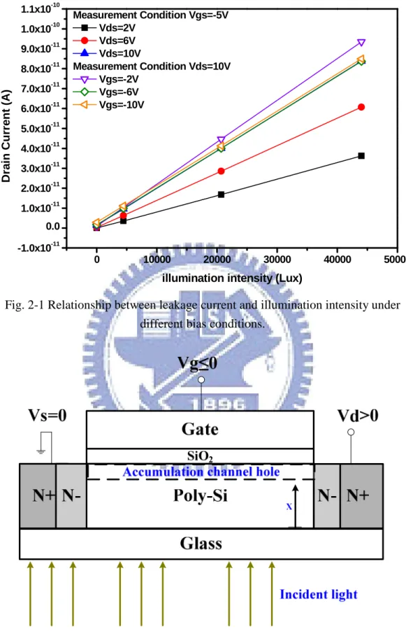
Definition of Unit-Lux Current
The relationships between leakage current and illumination intensity under different bias conditions are shown in Fig. 2-1. They all exhibit good linear dependence. The same linear dependence was observed in the case of front light
illumination in the previous paper [4]. The slope of the current-Lux curve was firstly
named as Unit-Lux Current or ULC in abbreviation, and used as an important index for analyzing the photosensitivity of LTPS TFTs. The meaning of ULC is the photo leakage current induced per unit-photo lux.
In this thesis, we use the same definition of ULC in the analysis for the backlight photosensitivity of LTPS TFTs to study the factors that influence the photo leakage current like bias conditions, temperatures, and defect states of LTPS TFTs under back light illumination in detail. As shown in Fig. 1-1, the channel region is block by the gate metal and not shined by the front light. Thus, we further compare the results of back light illumination to those of front light and discuss their differences.
2.2
Experiment Method
The cross section of the TFT device under back light illumination is shown in Fig. 2-2. Nowadays, the light emitting diode (LED) is more and more used as the backlight source of LCD to reduce the power and module thickness. Therefore, we use LED as the back light source in our experiments. In spite of passing through the glass substrate and probably the buffer oxide, the back light intensity hardly decreases
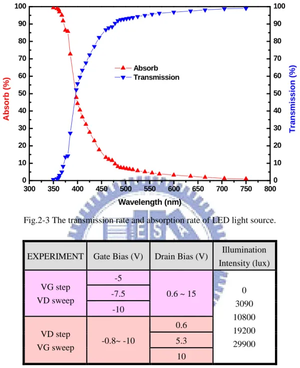
because the effect of the glass substrate and the buffer oxide on transmission is too little. On the other hand, the silicon film can absorb the back light to an amount. Fig. 2-3 shows the transmission and absorption rate of light at different wavelengths after
passing a silicon film with thickness of 65nm according to formula Iv(x) = Ivo exp(-κ
x), where Ivo and Iv(x) are the input intensity and the intensity at distance x,
respectively, κis the absorption coefficient, and x is the propagating distance [5].
Based on the calculation, we know the total intensity decreases up to 10% when the light comes to the channel surface of the TFT. However, the intensity of the short wavelength light, which contributes a lot of the electron-hole pair excitation, decreases drastically. The photo current might reduce more than 10% owing to this fact.
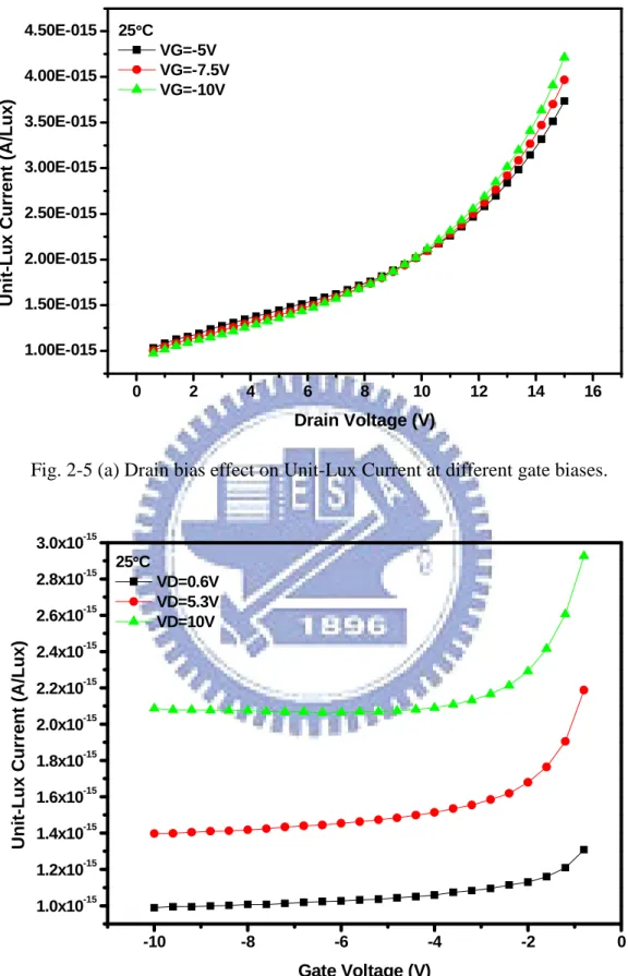
The photo leakage current (Iphoto) is measured at different bias conditions to study its field effect. Table 2-1 lists the measurement conditions of the gate and drain bias in detail. Two types of curves are measured, namely, with fixed the drain voltage (VD) as the gate voltage (VG) sweeping and with fixed VG and changing VD. In addition, the above two cases of measurement is repeated at various temperatures.
2.3
Behaviors of Unit-Lux Current
The relationship between Iphoto and illumination intensity under different drain biases or gate biases are shown in Fig. 2-4. It is clearly seen that the linearity retains whatever the bias condition changes, but only the slope varies, which preserves the privilege of using ULC as the index for our analysis. Fig. 2-5(a) and (b) demonstrate the drain bias effect and gate bias effect on ULC, respectively. It is noticed that drain bias affects the photo leakage current in an anomalous way, but the change of ULC is not obvious with respect to the gate bias. These two behaviors will be further
discussed in Section 2.4.
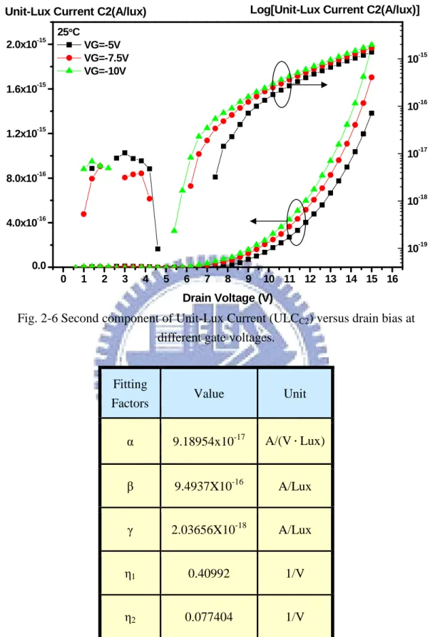
Referring to Fig. 2-5(a), it is observed that when drain voltage VD is lower than
8V, ULCincreases linearly with drain bias [6], and while VD is large enough, ULC
increases with drain bias more rapidly. In the case of front light illumination, this phenomenon was also observed and the front light ULC was separated into two
different parts [4]. Specifically, the first component is defined as ULCC1 which
increases with drain bias and independent of gate bias, and the second component is
defined as ULCC2 which is the total ULC subtracting ULCC1. Here, in a similar way,
we plot ULCC2 in Fig. 2-6. It is apparent that the log [ULCC2] increases with drain
bias linearly, indicating that ULCC2 increases with drain bias exponentially when
drain voltage VD is large enough. Therefore, the back light ULC can be expressed by a linear combination of these two components:
) exp( ) ( 1 2 2 1 VG VD VD ULC ULC ULC C C
η
η
γ
β
α
+ + − = + = (2.1)β
α
+ = VD ULCC1 (2.2) ) exp( 1 2 2 VD VG ULCC =γ η −η (2.3)where α,β,γ,η1 and η2 are all fitting parameters. α and β correspond
to the linear drain voltage dependence and the zero drain bias offset of ULCC1,
respectively. γ is the scaling factor of ULCC2, while η1 and η2 are the parameters
about the exponential dependence on drain bias and negative gate bias of ULCC2. The
values of fitting factors α,β,γ,η1 and η2 are listed in Table 2-2. As shown in Fig.
2-7, the empirical formula fits the experimental data very well.
2.4
Mechanisms of Unit-Lux Current
In this section, we discuss the results of the above two kinds of measurement conditions. When the gate bias is fixed, we figure that the drain region of the TFT is
biased to a situation similar to the abrupt p+n- junction. In this case, the lateral
depletion region increases linearly with drain bias [7]. As the drain bias is fixed, the
lateral depletion region is fixed. The more negative gate voltage can increase the concentration of the channel holes but the junction is hardly changed because the concentration is high enough. Thus the gate bias dependence of Unit-Lux Current is not obvious.
In equation 2.1, we separate the Unit-Lux Current into two parts. As the drain
bias is lower than 8V, which corresponds to ULCC1, the lateral electric field is small.
Referring to Fig.2-8(a), the energy band is almost flat at small VD. The main mechanism is proposed to be the excess carrier diffusion. When device is under the back light illumination, electron-hole pairs are generated. A part of electrons jump to the conduction band from the defects because of the thermionic emission effect.
Therefore, the dominant mechanism of ULCC1 is excess carrier diffusion and
thermionic emission [8]. On the other hand, as drain bias is large enough, which case
corresponds to ULCC2, the lateral electric field is large. Referring to Fig. 2-8(b), the
energy band is steep. The main mechanism is proposed to be the excess carrier drift in
the large electric field, which results in the field emission (or tunneling) [9]. A part of
electrons are tunneling from the trap to the conduction band. Therefore, the dominant
mechanism of ULCC2 is excess carrier drift and field emission (or tunneling).
To further confirm the proposed mechanisms, the temperature effect of ULC is taken into account. We again confirm that the correlation between Iphoto and illumination intensity at different temperature is still linear before the extraction of Unit-Lux Current. Fig. 2-9 shows the relationships between leakage current and
illumination intensity under different temperatures of 25, 35, 45, and 55 oC under the
bias condition of (VD, VG) = (10.2V, -7.5V). As can be seen, all the curves stay linear.
Fig. 2-10 shows drain bias dependences of Unit-Lux Current at different
temperatures. The ULC is significantly offset by temperature. By separating ULCC2
from total ULC, we can plot ULCC2 at different temperatures in Fig. 2-11. As can be
seen, all lines overlap completely in same place, which means that ULCC2 is
temperature independent.
Then, we further analyze on the temperature dependence of ULCC1. Both
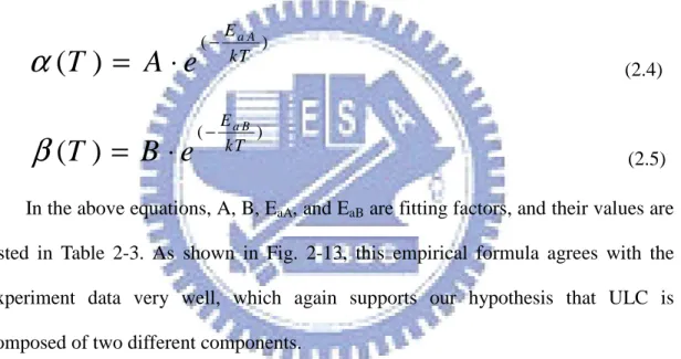
parameters α and β are plotted as the functions of temperature in Fig. 2-12. We find that these two parameters increase with 1/kT exponentially and can be expressed as follow: ( )
( )
a A E kTT
A e
α
=
⋅
− (2.4) ( )( )
a B E kTT
B e
β
= ⋅
− (2.5)In the above equations, A, B, EaA, and EaB are fitting factors, and their values are
listed in Table 2-3. As shown in Fig. 2-13, this empirical formula agrees with the experiment data very well, which again supports our hypothesis that ULC is composed of two different components.
Since the temperature only affects the ULCC1, it is consistent with the
mechanism of thermionic emission. As for the temperature independence of ULCC2, it
is because the field emission dominates the photo current over the thermionic emission.
2.5
Comparison of Front and Back Light Effects
The similar behaviors of the front light ULC and back light ULC indicate that the mechanism is basically the same. However, we can still find some differences. As
shown in Fig. 2-14, the magnitudes of the ULC are different. The main reason is that the sensing regions of illumination are different. The gate metal shields the front light so that the front light sensing region is only in the LDD region. As for the back light sensing, the region includes both the channel and LDD. Therefore, more electron-hole pairs are generated under the back light illumination. The involvement of the channel
region in the back light sensing also explains that the effect of gate voltage on ULCC2
for the front light case is larger than that for the case of back light, as shown in Fig 2-15 and table 2-2.
0 10000 20000 30000 40000 50000 -1.0x10⁻¹¹ 0.0 1.0x10⁻¹¹ 2.0x10⁻¹¹ 3.0x10⁻¹¹ 4.0x10⁻¹¹ 5.0x10⁻¹¹ 6.0x10⁻¹¹ 7.0x10⁻¹¹ 8.0x10⁻¹¹ 9.0x10⁻¹¹ 1.0x10⁻¹⁰ 1.1x10⁻¹⁰ D ra in C u rr e n t (A )
illumination intensity (Lux)
Measurement Condition Vgs=-5V Vds=2V Vds=6V Vds=10V Measurement Condition Vds=10V Vgs=-2V Vgs=-6V Vgs=-10V
Fig. 2-1 Relationship between leakage current and illumination intensity under different bias conditions.
300 350 400 450 500 550 600 650 700 750 800 0 10 20 30 40 50 60 70 80 90 100 0 10 20 30 40 50 60 70 80 90 100 T ra n s m is s io n ( % ) A b s o rb ( % ) Wavelength (nm) Absorb Transmission
Fig.2-3 The transmission rate and absorption rate of LED light source.
EXPERIMENT Gate Bias (V) Drain Bias (V) Illumination
Intensity (lux) VG step VD sweep -5 0.6 ~ 15 0 3090 10800 19200 29900 -7.5 -10 VD step VG sweep -0.8~ -10 0.6 5.3 10
0 10000 20000 30000 40000 50000 0.0 2.0x10⁻¹¹ 4.0x10⁻¹¹ 6.0x10⁻¹¹ 8.0x10⁻¹¹ 1.0x10⁻¹⁰ 1.2x10⁻¹⁰ 1.4x10⁻¹⁰ 1.6x10⁻¹⁰ 1.8x10⁻¹⁰ Ip h o to ( A )
illumination intensity (Lux)
Vg=-5V VD=0.6V VD=3V VD=5.4V VD=7.8V VD=10.2V VD=12.6V VD=15V
Fig. 2-4 (a) Photo leakage current at VG= -5V and VD=0.6V to 15V.
0 10000 20000 30000 40000 50000 0.0 2.0x10⁻¹¹ 4.0x10⁻¹¹ 6.0x10⁻¹¹ 8.0x10⁻¹¹ 1.0x10⁻¹⁰ 1.2x10⁻¹⁰ Ip h o to ( A )
illumination intensity (Lux)
Vd=5.3V VG=-10V VG=-8.4V VG=-6.8V VG=-5.2V VG=-3.6V VG=-2V VG=-0.4V
0 2 4 6 8 10 12 14 16 1.00E-015 1.50E-015 2.00E-015 2.50E-015 3.00E-015 3.50E-015 4.00E-015 4.50E-015 U n it -L u x C u rr e n t (A /L u x ) Drain Voltage (V) 25°°°°C VG=-5V VG=-7.5V VG=-10V
Fig. 2-5 (a) Drain bias effect on Unit-Lux Current at different gate biases.
-10 -8 -6 -4 -2 0 1.0x10⁻¹⁵ 1.2x10⁻¹⁵ 1.4x10⁻¹⁵ 1.6x10⁻¹⁵ 1.8x10⁻¹⁵ 2.0x10⁻¹⁵ 2.2x10⁻¹⁵ 2.4x10⁻¹⁵ 2.6x10⁻¹⁵ 2.8x10⁻¹⁵ 3.0x10⁻¹⁵ U n it -L u x C u rr e n t (A /L u x ) Gate Voltage (V) 25°°°°C VD=0.6V VD=5.3V VD=10V
0 1 2 3 4 5 6 7 8 9 10 11 12 13 14 15 16 0.0 4.0x10⁻¹⁶ 8.0x10⁻¹⁶ 1.2x10⁻¹⁵ 1.6x10⁻¹⁵ 2.0x10⁻¹⁵
Unit-Lux Current C2(A/lux) Log[Unit-Lux Current C2(A/lux)]
Drain Voltage (V) 25°°°°C VG=-5V VG=-7.5V VG=-10V 10-19 10-18 10-17 10-16 10-15
Fig. 2-6 Second component of Unit-Lux Current (ULCC2) versus drain bias at
different gate voltages.
Fitting
Factors Value Unit
α 9.18954x10⁻¹⁷ A/(V.Lux)
β 9.4937X10⁻¹⁶ A/Lux
γ 2.03656X10⁻¹⁸ A/Lux
η1 0.40992 1/V
η2 0.077404 1/V
-1 0 1 2 3 4 5 6 7 8 9 10 11 12 13 14 15 16 5.0x10⁻¹⁶ 1.0x10⁻¹⁵ 1.5x10⁻¹⁵ 2.0x10⁻¹⁵ 2.5x10⁻¹⁵ 3.0x10⁻¹⁵ 3.5x10⁻¹⁵ 4.0x10⁻¹⁵ 4.5x10⁻¹⁵ 25°°°°C VG=-5V VG=-7.5V VG=-10V Fitting VG=-5V VG=-7.5V VG=-10V U n it -L u x C u rr e n t (A /l u x ) Drain Voltage (V)
Fig. 2-7 Experiment data (symbols) and empirical formula (solid lines).
Fig. 2-8 (b) Proposed model of ULCC2 mechanism for LTPS TFTs. 0 10000 20000 30000 40000 50000 0.00E+000 2.00E-011 4.00E-011 6.00E-011 8.00E-011 1.00E-010 1.20E-010 1.40E-010 Ip h o to ( A )
illumination intensity (Lux)
(VD,VG)=(10.2V,-5V)
25°°°°C
35°°°°C
45°°°°C
55°°°°C
0 2 4 6 8 10 12 14 16 1.0x10⁻¹⁵ 1.5x10⁻¹⁵ 2.0x10⁻¹⁵ 2.5x10⁻¹⁵ 3.0x10⁻¹⁵ 3.5x10⁻¹⁵ 4.0x10⁻¹⁵ U n it -L u x C u rr e n t (A /L u x ) Drain Voltage (V) VG=-5V 25°°°°C 35°°°°C 45°°°°C 55°°°°C
Fig. 2-10 Drain bias dependence of Unit-Lux Current at different temperature.
0 2 4 6 8 10 12 14 16 10-18 10-17 10-16 10-15 Drain Voltage (V) VG=-5V 25°°°°C 35°°°°C 45°°°°C 55°°°°C
Log[Unit-Lux Current (A/Lux)] Unit-Lux Current (A/Lux)
0.0 1.0x10⁻¹⁵ 2.0x10⁻¹⁵ 3.0x10⁻¹⁵
Fig. 2-11 The second component of Unit-Lux-Current (ULCC2) versus drain bias with
35.0 35.5 36.0 36.5 37.0 37.5 38.0 38.5 39.0 9.15x10⁻¹⁷ 9.20x10⁻¹⁷ 9.25x10⁻¹⁷ 9.30x10⁻¹⁷ 9.35x10⁻¹⁷ 9.40x10⁻¹⁷ 9.45x10⁻¹⁷ 9.50x10⁻¹⁷ 9.55x10⁻¹⁷ α αα α(A/(V••••Lux)) 1/kT (1/eV) αααα 9.50x10⁻¹⁶ 1.00x10⁻¹⁵ 1.05x10⁻¹⁵ 1.10x10⁻¹⁵ 1.15x10⁻¹⁵ 1.20x10⁻¹⁵ ββββ(A/Lux) ββββ
Fig. 2-12 Dependence of parameters α and β on temperature.
Fitting
Factors Value Unit
A
1.223X10⁻¹⁶ A/(V.Lux)B
1.086X10⁻¹⁴ A/LuxE
aA 0.0071 eVE
aB 0.0626 eV0 2 4 6 8 10 12 14 16 1.0x10⁻¹⁵ 1.5x10⁻¹⁵ 2.0x10⁻¹⁵ 2.5x10⁻¹⁵ 3.0x10⁻¹⁵ 3.5x10⁻¹⁵ 4.0x10⁻¹⁵
U
n
it
-L
u
x
C
u
rr
e
n
t
(A
/L
u
x
)
Drain Voltage (V)
VG=-5V 25°°°°C 35°°°°C 45°°°°C 55°°°°C Fitting 25°°°°C 35°°°°C 45°°°°C 55°°°°CFig. 2-13 Experiment data (symbols) and empirical formula (solid lines).
0 2 4 6 8 10 12 14 16 1.0x10⁻¹⁵ 1.5x10⁻¹⁵ 2.0x10⁻¹⁵ 2.5x10⁻¹⁵ 3.0x10⁻¹⁵ 3.5x10⁻¹⁵ 4.0x10⁻¹⁵ 4.5x10⁻¹⁵ 5.0x10⁻¹⁵ 5.5x10⁻¹⁵ 6.0x10⁻¹⁵ 6.5x10⁻¹⁵ 7.0x10⁻¹⁵ 7.5x10⁻¹⁵ 8.0x10⁻¹⁵ 8.5x10⁻¹⁵ 9.0x10⁻¹⁵ U n it -L u x C u rr e n t (A /L u x ) Drain Voltage (V) FL VG=-5V FL VG=-7.5V FL VG=-10V BL VG=-5V BL VG=-7.5V BL VG=-10V
Fig. 2-15 Drain bias effect on Unit-Lux Current at different gate biases under front light illumination
Chapter3
Effects of the Defects Created by Hot
Carrier Stress
3.1
Degradation Mechanism and Stress Condition
Degradation of the electrical characteristics due to hot carrier effect is an important issue in TFTs application. Extensive investigation has shown that hot carrier induced defect states could be generated at the grain boundaries close to drain
junction [10-12]. In this thesis, we utilize this electric degradation to create defect
states and discuss the characteristics of photo-leakage current after the creation of these extra defects.
Fig. 3-1 shows the damage region after hot carrier stress. When a gate bias slightly greater than threshold voltage and a large drain bias applied on a TFT, a high electric fields from the voltage difference between gate and drain presents in the junction depletion region. This field accelerates the electron-hole pairs to “hot carriers” with high kinetic energy and strike the lattice structure in this region. Avalanche multiplication due to impact ionization takes place at the drain end of the channel, thus leaves large amount of tail state strain bond defects here.
This degradation phenomenon causes severe decrease on the device mobility, as shown in Fig. 3-2. IV curve after stress altered significantly in both on and off region. The leakage current increases because the defects act as a transient transfer centers for carriers conducting. In the on region, however, these defects trap carriers would decrease the amount of carriers which are collected by drain electrode.
In our experiment, we stressed our devices at VG = 3V, and VD = 16V, and measure them at different stress times of 25, 100, 500, 1000 sec. In the later section, we will show how the photo leakage current alters at different stress time. Table 3-1 lists the experiment conditions in detail. The devices are characterized in forward and reverse configurations, in which the damaged regions are put in the drain and source, respectively.
3.2
Analysis Unit-Lux Current after Stress
We again confirm that the correlations between Iphoto and illumination intensity at different stress times are still linear, as shown in Fig. 3-3, before extracting ULC and using it to discuss the results of forward and reverse measurement of ULC. With fixed the gate voltage (VG) as the drain voltage (VD) sweeping in the forward measurement, as shown in Fig. 3-4, we can see that the ULC increases and distorts slightly at lower drain bias with stress times. Compared to the unstressed device, the
ULCC2 of the devices operating at higher enough drain bias becomes less obvious and
the total ULC is smaller. On the other hand, for the reverse measurement, we can see that the ULC before and after stress remain the same, as shown in Fig. 3-5, which confirms the defects are only created near the drain side.
With fixed the drain voltage (VD) as the gate voltage (VG) sweeping, we again discuss the forward and reverse measurement of ULC. As shown in Fig. 3-6, generally speaking, ULC increases with stress time, but at the more negative gate voltages, ULC can be lower than its initial value. In Fig 3-7, the coincidence of the curves in the reverse measurement reconfirm that the source region is not damaged by hot carrier stress. Therefore, we can discuss the mechanism by considering only the drain side.
Fig. 3-8(a) and (b) show the proposed band diagrams along the channel direction near the drain region for a device after hot carrier stress under the condition of VG<0
at low and high drain biases, respectively. As the drain voltage is low, the dominant
conduction mechanism is thermionic emission. Referring to Fig. 3-8(a), when the LTPS TFT devices after hot carrier stress are under optical illumination, the additionally numerous electron-hole pairs from the created shallow tail states are generated in the lateral depletion region (Wd), as indicated by the red arrow. Before H.C. stress, this phenomenon is difficult to occur with the long wavelength light with low energy, because the energy is not enough for electrons to excite to conduction band. After stress, the created tail states locate closely to either conduction band or valance band, as indicated by the black solid line. In this case, the long wavelength light can also generate electron-hole pairs, as indicated by the red solid line arrow. The excess carriers are thermally excited to the conduction band, as indicated by the blue solid line arrow, and move in the conduction band and thus increase ULC.
However, there are mechanisms counteract the increase in the photo current. One of the mechanisms is the lattice scattering and coulomb scattering occurring in the path of conduction. The other mechanism is that a part of carriers can be captured by the shallow traps and then re-excited to the band, as indicated by the blue dotted line. It can slow down the speed of the excess carriers. These mechanisms are less effective than the increase of the photo-induced carriers from the extra states created, therefore, the photo leakage current obviously increases.
As for the high drain voltage, as shown in 3-8 (b), the dominant conduction mechanism is the field enhanced emission (or tunneling). Under illumination, the increment of electron-hole pairs at high VD should be the same as that in low drain, but instead, the reduced ULC is observed. In the unstressed device, most of the carriers excited from the tail states go to the conduction band via the field enhanced
emission, as indicated by the blue solid arrow. Nevertheless, in the H.C. stressed device, the carriers cannot tunneling directly to band because the possibility is be greatly reduced by the nearby tail state, as indicated by the blue dotted arrow.
Therefore, as shown in Fig. 3-4, the ULCC2 vanishes because of the lack of the
tunneling paths. As the stress time goes by, less and less tail states are created, and
thus ULC gently decreases with no trace of ULCC2 to occur.
3.3
Comparison Front Light with Back Light after
Stress
According to the previous paper [4], we know that the front light ULC on also
changes after H.C. stress. For both cases of front light and back light, the result of the reverse measurement after H.C. stress keeps same, which is consistent with the fact the defects are created near drain side.
In section 2.5, we explained that the back light ULC is larger than that of front light by sensing regions of illumination. As shown in Fig. 3-9, during the whole H.C. stress process, this phenomenon preserves at every stress time.
In the previous study of H.C. stress, it is explained that the tail states created in LDD near drain region. We again confirm the effect by comparing the change of ULC under front and back light illumination. If the defects are created in the LDD region, both the front and back lights can shine on them. In section 3.2, we explained that the
back light ULCC2 with respect to the effect of field enhanced emission (or tunneling)
is not obvious because the tail states can reduce tunneling effect. As shown in Fig
3-10, we can also see the ULCC2 under front light condition is not obvious after H.C
stress. Fig.3-11 shows the difference of ULC and fitted initial ULCC1 at different
This difference in ULC corresponds to the defects created by H.C. stress. We can see that the ULC difference for the back light illumination is never larger than that for the front light illumination, which is very different from the comparison of the initial front and back light ULC. For the same device after stress, the amounts and the locations of the created defects are all the same. It depicts that no defects are created in the channel illuminated by the back light. Furthermore, the ULC difference under back light illumination is even smaller than that under front light. It is attributed to the decrease of the back light intensity, especially for short wavelength light, through the silicon film as mentioned in section 2.2.
Fig. 3-1 Scheme of damage region in a LTPS TFT after hot carrier stress. -10 -5 0 5 10 10-16 10-15 10-14 10-13 10-12 10-11 10-10 10-9 10-8 10-7 10-6 10-5 10-4 10-3 D ra in C u rr e n t (A ) Gate Voltage (V) BL VD=16V VG=3V Before Stress VD=0.1V VD=10V After Stress VD=0.1V VD=10V
DC stress Condition :
Hot Carrier Stress VG=3(V), VD=16(V), VS=0(V)
Stress time = 0, 25, 100, 500, 1000 (sec)
Table 3-1(a) Experiment conditions for hot carriers stress
EXPERIMENT Gate Bias (V) Drain Bias (V) Illumination
Intensity (lux) VG step VD sweep -5 0.6 ~ 15 0 3090 10800 19200 29900 -7.5 -10 VD step VG sweep -0.8~ -10 0.6 5.3 10
Table 3-1(b) Measurement conditions for the photo leakage
0 10000 20000 30000 -1.0x10⁻¹¹ 0.0 1.0x10⁻¹¹ 2.0x10⁻¹¹ 3.0x10⁻¹¹ 4.0x10⁻¹¹ 5.0x10⁻¹¹ 6.0x10⁻¹¹ 7.0x10⁻¹¹ 8.0x10⁻¹¹ 9.0x10⁻¹¹ 1.0x10⁻¹⁰ 1.1x10⁻¹⁰ Ip h o to ( A )
illumination intensity (lux)
VG=-5V VD=10.2V Forward (BL) Stress 0s Stress 25s Stress 100s Stress 500s Stress 1000s
Fig. 3-3 (a) Relationship between leakage current and back light illumination intensity after different H.C. stress times in the forward measurement.
0 10000 20000 30000 -1.0x10⁻¹¹ 0.0 1.0x10⁻¹¹ 2.0x10⁻¹¹ 3.0x10⁻¹¹ 4.0x10⁻¹¹ 5.0x10⁻¹¹ 6.0x10⁻¹¹ 7.0x10⁻¹¹ 8.0x10⁻¹¹ 9.0x10⁻¹¹ 1.0x10⁻¹⁰ 1.1x10⁻¹⁰ Ip h o to ( A )
illumination intensity (lux)
VG=-5V VD=10.2V Reverse (BL) Stress 0s Stress 25s Stress 100s Stress 500s Stress 1000s
Fig. 3-3 (b) Relationship between leakage current and back light illumination intensity after different H.C. stress times in the reverse measurement.
0 2 4 6 8 10 12 14 16 1.0x10⁻¹⁵ 1.5x10⁻¹⁵ 2.0x10⁻¹⁵ 2.5x10⁻¹⁵ 3.0x10⁻¹⁵ 3.5x10⁻¹⁵ 4.0x10⁻¹⁵ 4.5x10⁻¹⁵ 5.0x10⁻¹⁵ 5.5x10⁻¹⁵ 6.0x10⁻¹⁵ U n it -L u x C u rr e n t (A /l u x ) Drain Voltage (V) VD=0.6V~10V VG=-5V Forward (BL) Stress 0s Stress 25s Stress 100s Stress 500s Stress 1000s
Fig. 3-4 Drain bias dependence of ULC at different H.C. stress times measured in the forward mode.
0 2 4 6 8 10 12 14 16 1.0x10⁻¹⁵ 1.5x10⁻¹⁵ 2.0x10⁻¹⁵ 2.5x10⁻¹⁵ 3.0x10⁻¹⁵ 3.5x10⁻¹⁵ 4.0x10⁻¹⁵ 4.5x10⁻¹⁵ 5.0x10⁻¹⁵ 5.5x10⁻¹⁵ 6.0x10⁻¹⁵ 6.5x10⁻¹⁵ U n it -L u x C u rr e n t (A /l u x ) Drain Voltage (V) VD=0.6V~10V VG=-5V (BL) Reverse Stress 0s Stress 25s Stress 100s Stress 500s Stress 1000s
Fig. 3-5 Drain bias dependence of ULC at different H.C. stress times measured in the reverse mode. -11 -10 -9 -8 -7 -6 -5 -4 -3 -2 -1 0 3.0x10⁻¹⁵ 3.5x10⁻¹⁵ 4.0x10⁻¹⁵ 4.5x10⁻¹⁵ 5.0x10⁻¹⁵ U n it -L u x C u rr e n t (A /l u x ) Gate Voltage (V) VG=-10~-0.6 VD=10V Forward (BL) Stress 0s Stress 25s Stress 100s Stress 500s Stress 1000s
Fig. 3-6 Gate bias dependence of ULC at different H.C. stress times measured in the forward mode.
-10 -8 -6 -4 -2 0 3.0x10⁻¹⁵ 3.5x10⁻¹⁵ 4.0x10⁻¹⁵ 4.5x10⁻¹⁵ U n it -L u x C u rr e n t (A /l u x ) Gate Voltage (V) VG=-10~-0.6 VD=10V (BL) Reverse Stress 0s Stress 25s Stress 100s Stress 500s Stress 1000s
Fig. 3-7 Gate bias dependence of ULC at different H.C. stress times measured in the reverse mode.
Fig. 3-8 (a) A proposed model of ULC mechanism for LTPS TFTs after H.C. stress at low drain bias.
Fig. 3-8 (b) A proposed model of ULC mechanism for LTPS TFTs after H.C. stress at high drain bias.
0 250 500 750 1000 1.0x10⁻¹⁵ 2.0x10⁻¹⁵ 3.0x10⁻¹⁵ 4.0x10⁻¹⁵ 5.0x10⁻¹⁵ 6.0x10⁻¹⁵ U n it -L u x C u rr e n t (A /l u x ) Stress Time (s)
Hot Carrier Stress (Forward)
FL BL VD=0.6V VD=0.6V VD=4.2V VD=4.2V VD=7.8V VD=7.8V VD=11.4V VD=11.4V VD=15V VD=15V
Fig. 3-9 Relationship between ULC and stress time after different H.C. stress measured in the forward mode.
0 2 4 6 8 10 12 14 16 1.0x10⁻¹⁵ 1.5x10⁻¹⁵ 2.0x10⁻¹⁵ 2.5x10⁻¹⁵ 3.0x10⁻¹⁵ 3.5x10⁻¹⁵ 4.0x10⁻¹⁵ U n it -L u x C u rr e n t (A /l u x ) Drain Voltage (V) VD=0.6V~10V VG=-5V
(FL)
Forward Stress 0s Stress 25s Stress 100s Stress 500s Stress 1000sFig. 3-10 Drain bias dependence of ULC at different H.C. stress times measured in the forward mode under front light condition.
0 2 4 6 8 0.0 4.0x10⁻¹⁶ 8.0x10⁻¹⁶ 1.2x10⁻¹⁵ 1.6x10⁻¹⁵ 2.0x10⁻¹⁵ Er ro r (A /L u x ) Drain Voltage (V) Error=ULC(t)-ULCC1Fit(0)
Front Light Back Light
Stress (25)-Stress(0) Stress (25)-Stress(0) Stress (100)-Stress(0) Stress (100)-Stress(0) Stress (500)-Stress(0) Stress (500)-Stress(0) Stress (1000)-Stress(0) Stress (1000)-Stress(0)
Fig. 3-11 Tail state enhance photo leakage current after different stress time at different illumination in the forward mode.
Chapter4
Effects of the Defects Created by Self
Heating Stress
4.1
Degradation Mechanism and Stress Condition
LTPS TFTs, in most applications, are fabricated on glass substrates with poor thermal conductivity. Therefore, as the applied VG and VD are high, the heat resulting from the high current flow and voltage difference in the channel may be difficult to dissipate. The accumulated heat causes the Si–H bonds to break, which in turn increases the deep states dangling bond in the channel. This degradation is known as
Self Heating effect [13-14].
The thermal degradation phenomenon in the self heating stress may induce a lot
of defect states in the whole poly-Si thin film [15]. However, in this thesis, we use a
model of defect distribution in the thin film as shown in Fig. 4-1 to discuss the photo effect for simplification.
The states created by self heating stress apparently affect the transfer characteristic of the device mainly in on and sub-threshold region. Fig. 4-2 shows the ID-VG curve of LTPS TFT after self heating stress. In addition to the lowered mobility, serious threshold voltage shift is the most important phenomenon induced by the self heating stress. It depicts that there are numerous deep states in the mid gap to be filled before the device is turned on.
In our experiment, we stressed our device at VG = 15V, and VD = 15V, and measured at different stress times of 1, 5, 50, 200, 600, and 1000 sec. Table 4-1 lists
the experiment conditions in detail. In our measurements, the devices are characterized in forward and reverse configurations, in which the damaged regions are put in the different ways.
4.2
Analysis Unit-Lux Current after Stress
We once more confirm that the correlations between Iphoto and illumination intensity at different stress times are still linear, as shown in Fig. 4-3, before extracting ULC and using it to discuss the results of forward and reverse measurement of ULC. With fixed VG as VD sweeping in the forward measurement, the ULC is shown in Fig. 4-4. Compared to the unstressed device, we can see that the ULC
decreases at higher drain bias with stress time, while ULCC1 of the devices does not
change significantly. On the other hand, for the reverse measurement, as shown in
Fig. 4-5, we can see that the ULC increases with stress time and ULCC2 changes
significantly at high drain bias. Based on the previous study [3], the sensing region of
the front light is only in the drain region. The results of back light ULC in reverse measurement suggest the severe degradation after self-heating stress.
With fixed VD as VG sweeping, we again discuss the forward and reverse measurements of ULC. The result of forward measurement is shown in Figure 4-6. It is pointed out that the ULC decreases with stress time and the gate field has little effect on it. Contrarily, for the result of reverse measurement shown in Figure 4-7, which corresponds to the change at the source junction, the photo leakage current increases just like the case of H.C. stress. These results indicate that the defects created by S.H. stress in the source and drain regions are very different. We take them into account to discuss the mechanism of S.H in the following paragraphs by considering the different kinds of the defects on the drain and source sides.
Considering the drain region of the poly-Si TFT after self heating degradation, we propose the band diagrams along the channel direction near the drain region for a device after self heating stress under the condition of VG<0 at low and high drain biases as shown in Fig. 4-8(a) and (b), respectively. During self heating stress, the high temperature makes the poly-Si film release hydrogen atoms and causes plenty of dangling bonds, which is well known as deep states. These deep states located near the middle level in the lateral depletion region can be very helpful to the recombination of the electron-hole pairs generated by irradiation. This is believed to be the reason why the total current is reduced after S.H. stress.
As for the source region, Fig. 4-9(a) and (b) show our proposed band diagrams along the channel direction near the source region for a device after self heating stress under the condition of VG<0 at low and high drain biases, respectively. The additionally numerous electron-hole pairs from additionally created shallow tail states are generated in the lateral depletion region (Wd), as indicated by the red arrow. Before S.H. stress, this phenomenon is difficult to occur for the long wavelength light with low energy. Without these tail states, long wavelength light does not have enough energy to excite the electrons to the conduction band. After stress, the tail states care created near to either conduction band or valance band, as indicated by the black solid line in Fig. 4-9. In such a case, the long wavelength light can also generate electron-hole pairs through the tail states, as indicated by the red solid line arrow, followed by the thermal excitation or tunneling to the conduction band, as indicated by the blue solid line arrow, and move in the conduction band. Therefore, the photo leakage current obviously increases due to the extra photo-induced carriers excited by the lower energy part of light through the states created.
4.3
Comparison Front Light with Back Light ULCs
after Stress
According to the previous paper [5], we know that the front light ULC also
changes after S.H. stress. Here we compare the cases of front light and back light to study the effect of S.H. stress in the poly-Si TFT. For the forward measurement after S.H. stress, both the back light ULC shown in Fig. 4-3(a) and the front light ULC shown in Fig. 4-10(a) decrease with the stress time. Nevertheless, the results of the reverse measurement after S.H. stress are very different, as shown in Fig. 4-3(b) (back light ULC) and Fig. 4-10(b) (front light ULC). Therefore, we focus on the difference of back light and front light ULCs measured in the reverse mode. In Fig. 4-11, we compare the reverse measure of back light ULC with the front light one in the same scale. It is observed that the change of ULC is not obvious under front light illumination with stress time. On the contrary, the ULC increases significantly under back light condition with stress time. It indicates that the back light illumination can shine on the defects to generate the photo current, but those defects cannot be illuminated by the front light.
Even though what the information revealed in the reverse measurement is about the degradation mechanism is only proven for front light ULC, we assume it is also valid for the back light ULC. Therewith, we explain the reason why the ULC increases only under back light illumination rather than front light is that most of the tail states created near the source region locate under gate metal and thus they are only irradiated by the back light instead of the front light.
The degradation model for S.H. stress in TFT structure is proposed as shown in Fig. 4-12 to demonstrate the roles of defects in self heating stress. Self heating stress can create both tail and interface states near source region. High electric fields from
the voltage difference between gate and source presents under gate metal. This field accelerates the carriers to be “hot” with high kinetic energy and strikes the lattice structure in this region, and thus leaves large amount of tail state strain bond defects in this region. The spatial distribution of the interfacial states depends on the intensity of the electric field along channel from source to drain. Therefore, more tail states and interface states created along poly-Si channel near the source region.
This spatial distribution of defects after S.H. stress near the source region is firstly observed by the study of back light ULC. It provides complementary information to the study of the self heating stress.
Fig. 4-1 Scheme of damage region in a LTPS TFT after self heating stress -10 -5 0 5 10 10-15 10-14 10-13 10-12 10-11 10-10 10-9 10-8 10-7 10-6 10-5 10-4 10-3 D ra in C u rr e n t (A ) Gate Voltage (V) BL VD=15V VG=15V Before Stress VD=0.1V VD=10V After Stress VD=0.1V VD=10V
DC stress Condition :
Self Heating Stress VG=15(V), VD=15(V), VS=0(V)
Stress time = 0, 1, 5, 50, 200, 600, 1000 (sec)
Table 4-1(a) Experiment conditions for self heating stress
EXPERIMENT Gate Bias (V) Drain Bias (V) Illumination
Intensity (lux) VG step VD sweep -5 0.6 ~ 15 0 3090 10800 19200 29900 -7.5 -10 VD step VG sweep -0.8~ -10 0.6 5.3 10
Table 4-1(b) Measurement conditions for the photo leakage
0 10000 20000 30000 0.0 2.0x10⁻¹¹ 4.0x10⁻¹¹ 6.0x10⁻¹¹ 8.0x10⁻¹¹ Ip h o to ( A )
illumination intensity (lux)
VG=-5V VD=10.2V Forward (BL) Stress 0s Stress 1s Stress 5s Stress 50s Stress 200s Stress 600s Stress 1000s
Fig. 4-3 (a) Relationship between leakage current and back light illumination intensity after different S.H. stress times in the forward measurement
0 10000 20000 30000 0.0 2.0x10⁻¹¹ 4.0x10⁻¹¹ 6.0x10⁻¹¹ 8.0x10⁻¹¹ 1.0x10⁻¹⁰ 1.2x10⁻¹⁰ Ip h o to ( A )
illumination intensity (lux)
VG=-5V VD=10.2V Reverse (BL) Stress 0s Stress 1s Stress 5s Stress 50s Stress 200s Stress 600s Stress 1000s
Fig. 4-3 (b) Relationship between leakage current and back light illumination intensity after different S.H. stress times in the reverse measurement
0 2 4 6 8 10 12 14 16 1.00x10⁻¹⁵ 1.25x10⁻¹⁵ 1.50x10⁻¹⁵ 1.75x10⁻¹⁵ 2.00x10⁻¹⁵ 2.25x10⁻¹⁵ 2.50x10⁻¹⁵ 2.75x10⁻¹⁵ 3.00x10⁻¹⁵ 3.25x10⁻¹⁵ 3.50x10⁻¹⁵ 3.75x10⁻¹⁵ 4.00x10⁻¹⁵ 4.25x10⁻¹⁵ 4.50x10⁻¹⁵ 4.75x10⁻¹⁵ 5.00x10⁻¹⁵ U n it -L u x C u rr e n t (A /l u x ) Drain Voltage (V) VD=0.6~15V VG=-5V BL Forward Stress 0s Stress 1s Stress 5s Stress 50s Stress 200s Stress 600s Stress 1000s
Fig. 4-4 Drain bias dependence of ULC at different S.H. stress times measured in the forward mode
0 2 4 6 8 10 12 14 16 1.0x10⁻¹⁵ 2.0x10⁻¹⁵ 3.0x10⁻¹⁵ 4.0x10⁻¹⁵ 5.0x10⁻¹⁵ 6.0x10⁻¹⁵ 7.0x10⁻¹⁵ 8.0x10⁻¹⁵ U n it -L u x C u rr e n t (A /l u x ) Drain Voltage (V) VD=0.6~15V VG=-5V BL Forward Stress 0s Stress 1s Stress 5s Stress 50s Stress 200s Stress 600s Stress 1000s
Fig. 4-5 Drain bias dependence of ULC at different S.H. stress times measured in the reverse mode -10 -8 -6 -4 -2 0 2.25x10⁻¹⁵ 2.50x10⁻¹⁵ 2.75x10⁻¹⁵ 3.00x10⁻¹⁵ 3.25x10⁻¹⁵ U n it -L u x C u rr e n t (A /l u x ) Gate Voltage (V) VG=-10~-0.6V VD=10V BL Forward Stress 0s Stress 1s Stress 5s Stress 50s Stress 200s Stress 600s Stress 1000s
Fig. 4-6 Gate bias dependence of ULC at different S.H. stress times measured in the forward mode
-10 -8 -6 -4 -2 0 2.0x10⁻¹⁵ 3.0x10⁻¹⁵ 4.0x10⁻¹⁵ 5.0x10⁻¹⁵ 6.0x10⁻¹⁵ 7.0x10⁻¹⁵ 8.0x10⁻¹⁵ U n it -L u x C u rr e n t (A /l u x ) Gate Voltage (V) VG=-10~-0.6V VD=10V BL Reverse Stress 0s Stress 1s Stress 5s Stress 50s Stress 200s Stress 600s Stress 1000s
Fig. 4-7 Gate bias dependence of ULC at different S.H. stress times measured in the reverse mode
Fig. 4-8 (a) A proposed model of ULC mechanism for LTPS TFTs after S.H. stress at low drain bias near drain side
Fig. 4-8 (b) A proposed model of ULC mechanism for LTPS TFTs after S.H. stress at high drain bias
Fig. 4-9 (a) A proposed model of ULC mechanism for LTPS TFTs after S.H. stress near source side at low drain bias
Fig. 4-9 (b) A proposed model of ULC mechanism for LTPS TFTs after S.H. stress near source side at high drain bias
0 10000 20000 30000 40000 50000 0.0 2.0x10⁻¹¹ 4.0x10⁻¹¹ 6.0x10⁻¹¹ 8.0x10⁻¹¹ 1.0x10⁻¹⁰ 1.2x10⁻¹⁰ Ip h o to ( A )
illumination intensity (lux)
VG=-5V VD=10V Forward (FL) Stress 0s Stress 1s Stress 5s Stress 50s Stress 200s Stress 600s Stress 1000s Fig. 4-10 (a) Relationship between leakage current and front light illumination