國
立
交
通
大
學
電機學院 IC 設計產業研發碩士班
碩 士 論 文
低電壓製程之電荷幫浦電路設計
Charge Pump Design in Low-Voltage CMOS
Process Technology
研 究 生:翁怡歆
指導教授:柯明道 教授
低電壓製程之電荷幫浦電路設計
Charge Pump Design in Low-voltage CMOS Technology
研 究 生:翁怡歆 Student:Yi-Hsin Weng
指導教授:柯明道 Advisor:Prof. Ming-Dou Ker
國 立 交 通 大 學
電機學院 IC 設計產業研發碩士班
碩 士 論 文
A Thesis
Submitted to College of Electrical and Computer Engineering National Chiao Tung University
in partial Fulfillment of the Requirements for the Degree of
Master in
Industrial Technology R & D Master Program on IC Design
July 2009
Hsinchu, Taiwan, Republic of China
i
低電壓製程之電荷幫浦電路設計
學生: 翁 怡 歆 指導教授: 柯 明 道 教授
國立交通大學 電機學院產業研發碩士班
摘要
電荷幫浦(charge pump circuits)能夠產生比輸入電壓(supply voltage)還要高的電位 以及比基準電位(GND)還要低的電位。現今電荷幫浦主要用於非揮發性記憶體中 (nonvolatile memory),用來抹除資料或者是寫入資料,此外,為了能夠符合一般家用電 規格,在LCD面板上同時也需要電荷幫浦來提高電壓以驅動面板的開關來達到色彩輸 出。
因此,此篇論文提出一個新的電荷幫浦的架構,其目的是為了在沒有受到閘極可 靠度(gate-oxide reliability)的影響之下,能夠減少漏電流(return-back leakage current)的產 生,同時透過模擬以及實做來實現電路。透過量測可以驗證新的電路架構是否能正常工 作以及是否有不錯的輸出效果。在1.8V的輸入電壓下,量測的輸出電位為8.8伏,此項結 果可以驗證新的電路架構比傳統的電荷幫浦有較好的效能。同時也驗證在減少漏電流的 情況以及沒有受到閘極可靠度的影響下,可以有效的提高輸出電壓。因此,新的電路架 構是適合在現今的低電壓以及低功率的積體電路上。
ii
Charge Pump Design in Low-voltage CMOS
Technology
Student: Yi-Hsin Weng
Advisor: Prof. Ming-Dou Ker
Industrial Technology R & D Master Program of
Electrical and Computer Engineering College
National Chiao Tung University
ABSTRACT
Charge pump circuits are usually used to generate voltages higher than the available supply voltage. It is applied widely in EEPROM or flash memories to program the floating-gate device.
A new charge pump circuit has been proposed to suppress the return-back leakage current without suffering the gate oxide reliability issue in low-voltage CMOS process. A test chip has been implemented in a 65-nm CMOS process to verify the proposed charge pump circuit with four pumping stages. By inserting a short turn-off period into the circuit operation of charge pump circuit, the return-back leakage current during the clock transition can be successfully suppressed in the new proposed charge pump circuit. The measured output voltage is around 8.8V with 1.8V supply voltage, which is better than the conventional charge pump circuit with the same pumping stages. Because of reducing the return-back leakage current and without suffering gate oxide reliability issue, the new proposed charge pump circuit is suitable for the applications in low-voltage and low-power CMOS IC products.
iii
introduces design background for charge pump circuit used in memories. Chapter 3 introduces the prior arts of charge pump circuits, and the summary is summarized all the problems solved and not solved. In Chapter 4, a new charge pump circuit, without the gate oxide reliability issue, reducing the return-back leakage current is presented, and the simulated results is also shown in this chapter. Finally, the efficiency and the return charge are introduced at the last. In chapter 5, the layout view and the measured result is displayed. At the final chapter, Chapter 6, recapitulates the major consideration of this thesis and concludes with suggestions for future investigation.
iv
A
CKNOWLEDGEMENTS致謝
兩年的碩士生涯,就這麼的過去了。曾經以為自己沒有辦法走過這一段,如今卻也 已要邁入結束。剛進入時的雄心壯志,早已被因不同的領域而遭受到的挫折消滅殆盡, 然僅存的是同學及學長的鼓勵與支持,以及父母背後默默的關心和男友貼心的扶持。 最感謝的還是柯明道柯教授,他是唯一第一個去找他面談之後就直接表達願意收我 的教授,同時,對我這個門外漢不厭其煩的細心指導,讓我收穫良多。請學長帶領我, 使我減少走冤枉路的時間,讓我能夠在兩年內順利的畢業。同時,幫我選擇適合我的論 文題目,除了可以讓我很容易上手外,更能隨時應用於工作上。如果說,我能夠順利的 畢業,最大的推手仍然是──老師。 在實驗室裡往往要耗上許多時日,感謝同學:Wuhuhu、佳琪、筱妊、彥良、溫董、 哲綸、小昀昀、昕爺、天哥、Kitty、阿黛爾、彥偉、育祥平時的搞笑讓我放鬆心情; 給我意見,讓我有一個穩定的方向及想法;難忘的生日驚喜,讓我突然驚覺,曾何幾時, 大家的感情已經這麼好。愛搞笑的學弟:佑達跟思漢,常常讓我啼笑皆非。貼心的學妹: 宛彥,在我忙碌的時候總能適時的伸出援手。若沒有這些同學、學弟妹,這兩年就會枯 燥無味。 遇上專業的問題,就要靠學長的幫忙。感謝 307 顏承正學長、林群佑學長、陳穩義 學長、小胖學長、竹立煒學長、帶我的小王學長、以及大小事都找他的小州哥,還有其 他 group 的學長:小凡學長、威文學長、罰三萬學長,以及其他我老是記不起來名字的 學長,不計其數,感謝讓我問白癡問題以及細心的提醒這個迷糊的我。謝謝這些學長平 時的幫忙,貼心的提醒以及幫我準備口試餐點,除了不好意思讓學長費盡心思的幫忙, 也不知道該如何去回報這些讓我的路途走個更平順的學長們。 在人生地不熟的地方,難得遇上高中同學,玉函及青玉,一起努力奮鬥。更要感謝 男友,黃彬,在我生活上的幫助,當搬家工人、當司機、當保母、當 GPS、當顧問、當 垃圾桶,儼然就是一個全方位專人執秘,讓我父母可以放心的讓我在新竹念書。最後要 感謝父母,翁勝義、黃秀菊,支持我的理想,提供想法以及三不五時怕我營養不良特地 從屏東用小黑貓宅配愛心;妹妹,依璇,在我分身乏術時,代替我回家陪伴父母,以及 即將要接手照顧我的寵物;我的寵物,髒髒,是在我回到無人的房間時,等我回家的…… 人,以及在我孤立無援時,勉強幫我壯膽子,雖然她只是一隻小老鼠。如今,即將要邁 向人生的另一個階段,也是我回饋社會,報答這些在我人生旅途上給我援助及支持的親 友! 出生之犢不畏虎,論文雖然力求完善,但謬誤之處在所難免,尚祈各位讀者不吝惜 賜予寶貴意見,使本論文能更加完善。 翁 怡 歆 謹 致 於 交大竹塹 已 丑 夏v
Index
摘要…… ... i ABSTRACT ... ii ACKNOWLEDGEMENTS ... iv Index…… ... vTable Captions ... vii
Figure Captions ... viii
Chapter 1 ... 1 Introduction ... 1 1.1 Motivation ... 1 1.2 Organization ... 2 Chapter 2 ... 3 Background ... 3
2.1 Introduction of Charge Pump Circuits ... 3
2.2 Applications of Charge Pump Circuits ... 5
Chapter 3 ... 7
Prior Arts of Charge Pump Circuits ... 7
3.1 Dickson Charge Pump Circuit ... 7
3.2 Charge Pump Circuit with Boostrapped Circuit ... 9
3.3 Floating Well Charge Pump Circuit (FWCP) ... 12
3.4 Charge Transfer Switches (CTS’s) Charge Pump ... 14
3.5 Charge Pump Circuits with Auxiliary Circuits ... 16
3.5.1 The Charge Pump Circuit with an Auxiliary Circuit ... 16
3.5.2 Charge Pump Circuit Using Auxiliary Circuits ... 19
3.6 Charge Pump Circuit Using Auxiliary MOSFET ... 20
3.7 New Four-Phase Charge Pump Circuit ... 21
3.8 Charge Pump Circuit Using All PMOS Devices ... 24
3.8.1 Charge Pump Circuit with Four-Phase Clock ... 24
3.8.2 The Six-Phase Charge Pump Circuit ... 27
3.9 The Charge Pump Circuit Without Gate Oxide Reliability Issue ... 29
3.10 Summary ... 32
Chapter 4 ... 33
vi
4.1 Introduction ... 33
4.2 The Operation of The New Proposed Charge Pump Circuit ... 33
4.3 Simulated Results ... 36
4.3.1 Simulations and Comparisons with the Prior Art [16] ... 36
4.3.2 Simulation of the Efficiency ... 41
4.3.3 Simulations for Different VDD ... 42
Chapter 5 ... 45
Measured Results of the New Proposed Charge Pump Circuit... 45
5.1 The Prior Art Circuit [16] ... 46
5.2 The New Proposed Charge Pump Circuit (this Work) ... 51
Chapter 6 ... 58
Conclusions and Future Works ... 58
6.1 Conclusions ... 58
6.2 Future Works ... 58
簡歷(vita) ... 62
vii
Table Captions
Table 3.1 The variation of the clock logic. ... 11
Table 3.2 The states of clocks in the different intervals. ... 22
Table 3.3 The clock logic table of the charge pump circuit using PMOS devices. ... 26
Table 3.3 The clock logic table for six-phase clock. ... 28
Table 4.1 The clock logic table. There are four periods of circuit operation in this new design. ... 35
viii
Figure Captions
Fig. 2.1 The method of the Cockcroft-Walton voltage multiplier [1]. ... 4
Fig. 2.2 It is Cockcroft-Walton voltage multiplier, and s, t, x, y, and z are the input impedances from their nodes [2]. ... 5
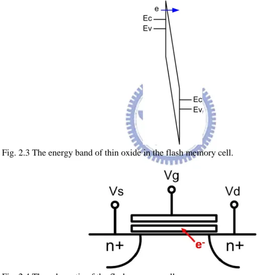
Fig. 2.3 The energy band of thin oxide in the flash memory cell. ... 6
Fig. 2.4 The schematic of the flash memory cell. ... 6
Fig. 3.1 Dickson charge pump circuit [2]. ... 9
Fig. 3.2 Dickson charge pump circuit realized with NMOS [6]. ... 9
Fig. 3.3 (a) A charge pump circuit without body effect, and (b) its clock waveforms. ... 12
Fig. 3.4 The boostrapped circuit in the charge pump circuit. ... 12
Fig. 3.5 (a) The floating-well charge pump circuit, (b) the cross section view of the one stage in this charge pump circuit, and (c) the variation waveform of clocks and the voltage potential of relative nodes. ... 14
Fig. 3.6 (a) The CTS’s charge pump circuit, and (b) a high-voltage clock generator. ... 16
Fig. 3.7 (a) The positive and (b) the negative charge pump circuits with an auxiliary circuit. (c) The steps of the first stage and (d) its cross section view. ... 19
Fig. 3.8 The waveforms of n1 node and the output voltage on the negative pump circuit. The supply voltage is 1.8V, pumping capacitor is 10pF, loading capacitor is 20pF, and the other devices are the same with this paper [10]... 19
Fig. 3.9 The charge pump circuit with two small circuits. ... 20
Fig. 3.10 The charge pump circuit by using auxiliary MOSFET. ... 21
Fig. 3.11 (a) The four-phase charge pump circuit, and (b) the clock waveforms. ... 23
Fig. 3.12 (a) The four-phase clock generator, (b) the delay circuit, and (c) high-voltage circuit (HVC). ... 24
Fig. 3.13 (a) The block diagram of the charge pump circuit using all PMOS devices, (b) The one stage of this charge pump circuit, and (c) its clock waveforms. ... 27
Fig. 3.14 (a) The six-phase charge pump circuit with four-stage, (b) the one stage circuit of this charge pump circuit, and (c) its clock waveforms. ... 29
Fig. 3.15 The charge pump pump circuit with no gate oxide reliability issue. ... 31
Fig. 3.16 The leakage path during the clock transitions. ... 31
Fig. 3.17 The simulation waveforms of the leakage currents. ... 31
Fig. 4.1 (a) New proposed charge pump circuit, and (b) the corresponding clock waveforms. ... 36
Fig. 4.2 The simulated voltage waveforms at the nodes 1~8 and the output (Vout) in the new proposed charge pump circuit with VDD of 1.8V. ... 38
Fig. 4.3 The leakage currents of the new proposed charge pump circuit. ... 38
ix
Fig. 4.5 The method used to estimate the return charge during the clock transition in the charge pump circuit. In this figure, two cases with rise/fall time of 1ns and 12 ns are demonstrated to approximately calculate the return charge with the formula of triangle
area. ... 39
Fig. 4.6 The estimated return charge of the charge pump circuits under with different rise/fall time in the clock signals (f=10MHz, VDD=1.8V). ... 40
Fig. 4.7 The simulated output voltage of the charge pump circuits under with different rise/fall time in the clock signals (f=10MHz, VDD=1.8V). ... 40
Fig. 4.9 The efficiencies of this work and the prior art circuit are in different supply voltages VDD with the 1MegΩ loading resistance. ... 43
Fig. 4.10 The output ripples of this work and prior art circuit are in different supply voltages VDD and without loading resistance (Rout). ... 44
Fig. 4.11 The output voltage decreases when the supply voltages are decreasing and without loading resistance (Rout). ... 44
Fig. 5.1 (a) The chip photograph about Bulk and DNW for the prior art circuit, and (b) the new proposed charge pump circuit, fabricated in a 65-nm CMOS process. ... 46
Fig. 5.2 The measurement setup of the prior art circuit. ... 47
Fig. 5.3 The clock waveforms of the prior art circuit. ... 48
Fig. 5.4 The measured outputs of the prior art circuit. ... 48
Fig. 5.5 The measurement results of each chip in (a) bulk process and (b) DNW process. ... 49
Fig. 5.6 The average output voltages about the prior art circuit with bulk process, DNW process, and simulation. ... 50
Fig. 5.7 The output voltages in different supply voltages VDD and without loading resistance (Rout). ... 50
Fig. 5.8 The measurement setup of this work. ... 52
Fig. 5.9 (a) The clock waveforms of this work, and (b) the time intervals in a clock period with 2ns of T_2 and T_4 time. ... 53
Fig. 5.10 The measured outputs of this work. ... 53
Fig. 5.11 The measured results of each chip in (a) the bulk process and (b) DNW process. ... 54
Fig. 5.12 The average output voltages about this work with bulk process, DNW process, and simulation. ... 55
Fig. 5.13 The output voltage in different supply voltages VDD and without loading resistance (Rout). ... 55
Fig. 5.7 The comparison of this work and the prior art circuit in the (a) bulk process and (b) DNW process (f=10MHz, VDD=1.8V, rise/fall time of ~2ns), with different loading resistance (Rout) at the output node. ... 56
Fig. 5.15 The comparison of the prior art circuit and this work in different supply voltages VDD and without loading resistance (Rout). ... 57
x
Fig. 5.16 The variations of the output voltage in different rise/fall times of the clocks and without loading resistance (Rout). ... 57 Fig. 6.1 The feedback loop of the charge pump circuit. ... 59
1
Chapter 1
Introduction
1.1
M
OTIVATIONCharge pump circuits are usually designed to generate voltage higher than the power supply voltage (VDD) or lower than the ground voltage (GND) in a chip. They are frequently used to provide a voltage higher than a power supply because high voltage level in a charge pump is generated by transferring charges to a capacitive load without any amplifiers or regular transformers. Most modern charge pump circuits are designed according to Dickson charge pump circuit, and the MOS transistors are utilized to transfer the charges from stage to stage.
Charge pump circuits are suitable for applications in low-voltage CMOS integrated circuits. It can be applied to the nonvolatile memories, such as EEPROM or flash memories, to write or to erase the floating-gate devices. Moreover, charge pump circuits are also used in power management blocks, the driver ICs for liquid-crystal-display (LCD) panels, and USB OTG (on-the-go).
Some problems of conventional charge pump circuit, such as threshold drop, body effect, junction breakdown, and gate-oxide reliability issues had been studied. Nevertheless, it suffered the return-back leakage current during the clock transitions.
In this work, by reducing the return-back leakage current, the new proposed charge pump circuit is suitable for the applications in low-voltage and low-power CMOS IC products without suffering gate oxide reliability issue.
2
1.2
O
RGANIZATIONThis thesis is organized into six chapters and this introduction is the first one. Chapter 2 introduces design background for charge pump circuit used in memories. Chapter 3 introduces the prior arts of charge pump circuits, and the summary is summarized all the problems solved and not solved. In Chapter 4, a new charge pump circuit, without the gate oxide reliability issue, reducing the return-back leakage current is presented, and the simulated results is also shown in this chapter. Finally, the efficiency and the return charge are introduced at the last. In chapter 5, the layout view and the measured result is displayed. At the final chapter, Chapter 6, recapitulates the major consideration of this thesis and concludes with suggestions for future investigation.
3
Chapter 2
Background
2.1
I
NTRODUCTION OFC
HARGEP
UMPC
IRCUITSThe first charge pump circuit is called the Cockcroft-Walton voltage multiplier with the purpose of generating steady potential nearly 800,000 volts to power the particle accelerator, performing the first artificial nuclear disintegration. Fig. 2.1 shows the method of Cockcroft-Walton voltage multiplier [1]. K1, K2, K3, X1, and X2 are the capacitors to storage
charges. S1, S1’, S2, S2’, S3, and S3’ are utilizedto transfer charges between the capacitors, and
VDD is the supply voltage. When connecting the switches of S1, S2, and S3, it is expected that
the voltage of n1 is VDD. After that, connecting switches of S1’, S2’, and S3’, the voltage of n1is
2VDD and the voltage of n2 is 2VDD. In the next reversal of the switches, the voltage of n3 is
2VDD. Finally, when it is connected with S1’, S2’, and S3’, the voltage of n4, which is equal to n3,
is 3VDD.From this method, Fig. 2.2 shows the basic Cockcroft-Walton voltage multiplier composed of capacitors (C), where Cs is the parasitic capacitor, diodes, and clocks (CLK and CLKB) to form the voltage multiplier [2].
When CLKB is low and the CLK is high,
D
V VDD
a= − . (2.1) At the next half period, CLKB is high and the CLK is low,
C x C VDD V VDD a D + × + − = , and (2.2) D V a b= − . (2.3) Next at another new period, CLKB is low and the CLK is high,
D
V VDD
4 D V 2 C s C C x C 1 VDD b ⎟− ⎠ ⎞ ⎜ ⎝ ⎛ + + + + = , and (2.5) D V b c= − . (2.6) And the next, CLKB is high and the CLK is low,
C x C VDD V VDD a D + × + − = , (2.7) D V a b= − , (2.8) D V 3 C y C C x C C s C C x C 1 VDD c ⎟⎟− ⎠ ⎞ ⎜⎜ ⎝ ⎛ + + + + + + + = , and (2.9) D V c d= − . (2.10) Finally, CLKB is low and the CLK is high,
D V VDD a= − , (2.11) D V 2 C s C C x C 1 VDD b ⎟− ⎠ ⎞ ⎜ ⎝ ⎛ + + + + = , (1.12) D V b c= − , (1.13) D V 4 C t C C s C C y C C x C C s C C x C 1 VDD d ⎟⎟− ⎠ ⎞ ⎜⎜ ⎝ ⎛ + + + + + + + + + + = , and (1.14) D V d e= − . (1.15) Hence, the input impedance increases in each node with the number of multiplying stages, it means the output voltage is decreased as the number of stage is increased. Therefore, the Cockcroft-Walton voltage multiplier is inefficient, when integrated into the chip, due to its large stray capacitance and high output impedance.
5
Fig. 2.2 It is Cockcroft-Walton voltage multiplier, and s, t, x, y, and z are the input impedances from their nodes [2].
2.2
A
PPLICATIONS OFC
HARGEP
UMPC
IRCUITSCharge pump circuits can generate the voltage higher than the power supply voltage (VDD) or lower than the ground voltage (GND) in a chip, usually used to write or erase data in nonvolatile memory[3]-[4]. Moreover, charge pump circuits are also used in power management blocks and the driver ICs for liquid-crystal-display (LCD) panels [5]. In mixed-mode circuit, it also needs to the charge pump circuit to generate higher voltage or negative voltage because there are more different supply voltage and VSS to be used.
Three main methods of programming and erasing data are Fowler-Nordheim tunneling (FN), band-to-band hot electron (BBHE), and channel hot-electron injection (CHEI).
In the program mode for NMOS, FN is that the gate terminal with the high voltage, where the source terminal is 0V and the drain terminal is floating, generate a high electron field to let the energy barrier of thin oxide like in Fig. 2.3, then the electron in the conduction band can tunnel through the triangular energy barrier to the floating gate shown in fig. 2.4. CHEI is that the device, where the gate terminal is the high voltage, the source terminal is 0V, and the drain terminal is a positive voltage smaller than the gate terminal, is turned on and then pinched up such that the hot-electron in the depletion region tunnel to the floating gate from the pinch up region. BBHE is that the drain terminal with the high voltage, where the gate terminal is
6
negative voltage and the source terminal is floating, let the energy band of the thin oxide be liked in Fig. 2.3 and make the electron tunneling to the floating gate.
In the erase mode for NMOS, there is only one way, FN, to erase. When the gate terminal is the negative voltage and the drain terminal is the small positive voltage, the electron in the floating gate will be rejected to tunnel to back the drain terminal. In another method, only the well of the cell with the high voltage let the electron in the floating gate tunnel to the well because of positive-negative electrode attracting.
Fig. 2.3 The energy band of thin oxide in the flash memory cell.
7
Chapter 3
Prior Arts of Charge Pump Circuits
3.1
D
ICKSONC
HARGEP
UMPC
IRCUITSince the Cockcroft-Walton voltage multiplier is inefficient, when it integrated into the chip due to its large stray capacitance and high input impedance. The Dickson charge pump circuit has been proposed to create a new voltage multiplier with higher efficiency, as shown in Fig. 3.1 [2], where CLK and CLKB are out of phase clocks, C is the pumping capacitor, Cs is the parasitic capacitor, Cout is the output capacitor loading, and RL is the output loading. When
the CLK is low (CLKB is high), the even-number diodes are turned off, and the odd-number diodes are turned on to transfer the charge from VDD to node a and node b to node c. Hence, the voltage of a, b, c, and d is Vd VDD a= − , (3.1) Vd 2 C C C 2 1 VDD b s − ⎟⎟ ⎠ ⎞ ⎜⎜ ⎝ ⎛ + + = , (3.2) Vd b c= − , and (3.3) Vd 4 C C C 4 1 VDD d s − ⎟⎟ ⎠ ⎞ ⎜⎜ ⎝ ⎛ + + = , (3.4)
where Vd is the voltage drop of diodes.
When the CLKB is low (CLK is high),the odd-number diodes are turned off, and the even-number diodes are turned on to transfer the charge from node a to node b and node c to node d. Hence, the voltage of a, b, c, and d is
s C C C VDD Vd VDD a + + − = , (3.5) Vd a b= − , (3.6) Vd 3 C C C 3 1 VDD c s − ⎟⎟ ⎠ ⎞ ⎜⎜ ⎝ ⎛ + + = , and (3.7)
8 Vd c
d= − . (3.8) Finally, the output voltage is shown in (3.9),
(
C C)
f NI Vd Vd VDD C C C N VDD Vout s out s + − − ⎥ ⎥ ⎦ ⎤ ⎢ ⎢ ⎣ ⎡ ⎟⎟ ⎠ ⎞ ⎜⎜ ⎝ ⎛ − + + = , (3.9)where the voltage drop in each stage due to the output current is
(
C C)
f NI ' V s out + = , (3.10)where N is the stage number, Iout is the output current, and f is the clock frequency [6].
Fig. 3.2 is shown the Dickson charge pump circuit realized with NMOS, and the diode-connected NMOS is utilized to transfer charge from input to output in each stage [6]. When the CLK is low (CLKB is high), m1, m3, and m5 are turned on (m2 and m4 kept off), the charge is transferred from VDD to node1, the charge in node 2, which is pumping higher by CLK, is transferred to node 3, and the charge in node 4 pumping to higher voltage is transferred to Vout. On the other hand, when the CLK is high (CLKB is low), m2 and m4 are turned on (m1 and m3 kept off), the voltage of node 1 and node 3 become higher. At this moment, the charge is transferred from node 1 to node 2, and charge in node 3 is transferred to node 4. Therefore, the output voltage of Dickson charge pump circuit is
∑
+ = ⎟⎟⎠ ⎞ ⎜⎜ ⎝ ⎛ − + = 1 1 N i ti s V C C C VDD Vout , (3.11)where Vti denotes the threshold voltage of the diode-connected NMOS in the ith stage, and N is the stage number. If the Cs is too small to ignore, the output voltage becomes
(
)
∑
+ = − = 1 1 N i ti V VDD Vout . (3.12)However, when each node is pumped higher, the threshold voltage in each NMOS becomes larger due to the body effect. Therefore, the efficiency of this circuit is decreased as the stage increases. Besides, it suffers overstress voltage across the gate oxide of devices when the voltages at each stage nodes are pumping higher. To avoid the gate-oxide overstress issue, the high-voltage device with thick gate oxide can be utilized for implementing such Dickson
9
charge pump circuit. However, the thick gate-oxide NMOS often has a high threshold voltage which somehow degrades the pumping efficiency.
Fig. 3.1 Dickson charge pump circuit [2].
Fig. 3.2 Dickson charge pump circuit realized with NMOS [6].
3.2
C
HARGEP
UMPC
IRCUIT WITHB
OOSTRAPPEDC
IRCUITTo restrain the body effect, Fig. 3.3(a) shows the charge pump circuit using boostrapped circuit [7], Fig. 3.3(b) shows its clock waveforms, and Table 3.1 shows the state of the clocks in different interval. This charge pump circuit is used PMOS to be the charge transfer device, as it has smaller leakage current than NMOS and its body and source can connect without extra masks.
The operations of this charge pump circuit are as following:
These four phases clock can be separated to six intervals, where the odd-number stages transfer charge at interval (1), (2), and (3), and even-number stages transfer charge at interval (4), (5), and (6).
At the interval (6) and (4)
10
turned off. Hence, the voltage of the n1 node is VDD-Vt0, where Vt0 is the threshold voltage of M0, and the voltage of the n2 node is 4VDD-Vt0.
At the interval (1) and (3)
When CLK2 is low and others are high, M0 is turned off, the voltage of n1 is rose to 2VDD-Vt0, but n2 is dropped to 3VDD-Vt0, M4 is turned on to transfer charge from n3 to the gate of M3, and other devices are turned off. The voltage of n1 is 2VDD-Vt0.
At the interval (2)
When CLK1 and CLK4 are high, and CLK2 and CLK3 are low, M1 is turned on to transfer charge from node 1 to node2, and M2 is turned off. At the same time, the voltage of node 1 still kept 2VDD-Vt0, and the voltage of node 2 is the same with node 1.
At the interval (5)
When CLK1 and CLK4 are low, and CLK2 and CLK3 are high, M0 is still turned on, n1is kept at VDD-Vt0, and n2 is also kept at 4VDD-Vt0. Moreover, M3 is turned on to transfer the voltage at n2 to n3, and others are kept off expect the transfer devices, M3, M5 and so on, at the even stage.
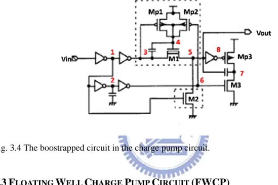
The boostrapped circuit is shown in Fig. 3.4. Using the boostrapped circuit can turn on the trsnsfer device certainly as the clocks connecting to the boostrapped circuit are at logic 0.
In the boostrapped circuit, when the input (Vin) is at logic 0, CLK is at logic 0, node 1 and node 6 are at logic 1, node 2 and node 3 are at logic 0, M3 is turned on to make node 7 be logic 0, Mp1 is turned on to let node 4 be at logic 1, and M1 will be turned on to transfer logic 0 from node 3 to node 5, where the capacitor storage charges since the difference voltages are at the two terminal of this capacitor. M2 is turned on to make node 5 be at logic 0 quickly, and then node 8 is at logic 1 to turn off Mp3.Therefor, the output voltage is at the mode of logic 0.
When the input is at logic 1, CLK is at logic 1, node 1 and node 6 are at logic 0, node 2 and node 3 are at logic 1, the M2 is turned off to cut off the current path from node 5, and Mp2 is turned on to keep the node 4 to hold at logic 1. Because node 3 becomes to logic 1, node 4
11
raises the voltage potential to the higher voltage and turn on M1 such that node 5 is with higher voltage potential. Therefore, Mp3 is turned on since node 8 is at logic 0; node 7 is at logic 1. Finally, the output voltage is with higher voltage than VDD.
In the Dickson charge pump circuit, the voltage gain at i stage is given by
(
)
( ) , ti bs s i gain V V C C VDD C V − + • = , (3.13)where Vti (Vbs) is the threshold voltage with Vbs bias at the i stage. This equation indicates that
the voltage gain is decreased and output voltage is not increased through using more stages due to the body effect. Although this prior art circuit can reduce the influence of the body effect, a threshold drop is still hold at NMOS and an extra circuit is used.
Table 3.1 The variation of the clock logic. Interval (1) (2) (3) (4) (5) (6) CLK1 1 1 1 0 0 0 CLK2 0 0 0 1 1 1 CLK3 1 0 1 1 1 1 CLK4 1 1 1 1 0 1 (a)
12
(b)
Fig. 3.3 (a) A charge pump circuit without body effect, and (b) its clock waveforms.
Fig. 3.4 The boostrapped circuit in the charge pump circuit.
3.3
F
LOATINGW
ELLC
HARGEP
UMPC
IRCUIT(FWCP)
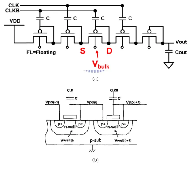
This charge pump circuits based on the Dickson charge pump circuit had been reported to enhance the pumping efficiency. Fig. 3.5(a) shows the floating-well charge pump circuit using the diode-connected PMOS as the charge transfer device [8].The operation of this charge pump circuit is similar to the Dickson charge pump circuit, and the only difference is that the bulks of device in this charge pump circuit are floating. From the formula of the threshold voltage,
[
bs f f]
0 t
t V V 2 2
V = +γ + φ − φ , (3.14) where Vt0 is the threshold voltage without body effect, γ is the body effect coefficient, Vbs is
the bias of the bulk and the source, and φf is the Fermi level. Since Vbs in all devices of the
13
Fig. 3.5 (b), and the threshold voltage is
[
diode f f]
0 t
te V V 2 2
V = +γ + φ − φ , (3.15) where Vdiode is the built-in potential of P+ to n-well diode. There are the parasitic diodes from
the diffusion layer (P+) and n-well in PMOS, and these diodes are always turned on, so the voltage of the bulks (n-well) changes during the clock transition. The relative illustration is shown in Fig. 3.5 (c). If the D voltage is higher than the S voltage, the Vbulk is D voltage-Vdiode.
On the other hand, if the S voltage is higher than the D voltage, the Vbulk is S voltage-Vdiode.
Although FWCP can reduce the influence of the body effect, it also induces the substrate current to disturb other circuits in the same chip.
(a)
14
(c)
Fig. 3.5 (a) The floating-well charge pump circuit, (b) the cross section view of the one stage in this charge pump circuit, and (c) the variation waveform of clocks and the voltage potential of relative nodes.
3.4
C
HARGET
RANSFERS
WITCHES(CTS’
S)
C
HARGEP
UMPFig. 3.6 (a) shows a charge pump circuit that can be assigned to control the CTS’s dynamically by using pass transistors MN’s and MP’s [9]. The CTS’s in this circuit can be turned off completely when clock transfers and be turned on easily by the backward control.
First, when CLK is low (CLKB is high), MD1 is turned on to transfer VDD to node 1, and then the voltage of node 1 is VDD-Vt1, where Vt is the threshold voltage of MD1. And the same
time, node 2 is pulled high to turn on MP1 (MD2is turned off), so MS1 is turn on to transfer charge to let the voltage of node 1 become VDD without the threshold drop. In this moment, MN2 is turned on to cut off MS2.
Second, when CLK is high (CLKB is low), the first stage is turned off and the second stage is turned on. Node 1 is pulled high to 2VDD, and MD2 is turned on to transfer charge from node 1 to node 2 (2VDD-Vt2, where Vt2 is the threshold voltage of MD2). In addition,
15
completely. Besides, MN2 and MP1 are turned off, and MN1 is turned on to close the switch MS1 to avoid the current returning back to the forward node.
Following this operation step by step, it has high efficiency in this charge pump circuit, but there is a threshold drop at the last stage due to the body effect. To overcome this limitation, this circuit is added another circuit, in Fig. 3.6 (b), at the last stage to compensate the threshold drop.
In this clock generator, when CLK is low, the voltage of node b is VDD to turn on M1 and M3, then the voltage of node a is VDD and CLKBh is VDD. At the next time, when CLK is high,
the voltage of node b is 0 and node a is pulled high to 2VDD to turn on M2, then the potential of node b becomes VDD from low; hence, M3 is turned off and M4 is turned on to discharge CLKBh to low. At the next period, CLK is low, the voltage of node a is back to VDD and the
voltage of node b rise to 2VDD to turn on M3, and the potential of CLKBh is 2VDD. And after
this period, CLKBh oscillates at 0 to 2VDD with 2VDD amplitude.
This charge pump circuit utilizes switches to transfer charge without the threshold drop, but it will has the threshold drop at the last stage without using the clock generator. However, it is a consideration where the bulk of M3 is connected, if using the clock generator in this charge pump circuit.
16
(b)
Fig. 3.6 (a) The CTS’s charge pump circuit, and (b) a high-voltage clock generator.
3.5
C
HARGEP
UMPC
IRCUITS WITHA
UXILIARYC
IRCUITS3.5.1 The Charge Pump Circuit with an Auxiliary Circuit
This charge pump circuit used small pump circuit to control the gate terminal of devices in the major pump circuit and used switches to control the bulk of the major device to avoid the body effect [10]. Fig. 3.7 (a) shows the negative pump circuit to generate the negative voltage, and Fig. 3.7 (b) shows the high positive pump circuit to generate the positive voltage.
For the small pump circuit
When CLKB=0 (CLK=1), Mu1 is turned on to let the potential of node 1 be GND+ |Vtp| and without the body effect, because Mus1 is turned on to connect bulk of Mu1 and node 1. When CLKB=1 (CLK=0), all the devices in the first stage are turned off, the voltage of node 1 is –VDD, and Mu2 and Mus2 are turned on to work the same function like the first stage. For the major pump circuit
In the ideal situation, when CLKB=0 (CLK=1), the M1 is turned on to make the potential of node n1 be GND+ |Vtp| due to the gate terminal of M1 is connected to negative voltage. At the same time, Ms1 is turned on to connect the bulk of M1 and node n1. However, in Fig. 3.7 (c), when CLK=1 (CLKB=0), M1 is turned on to let the potential of n1 be GND+ |Vtp|, and the
17
voltage of node n1 is dropped to –VDD+ |Vtp| instantly through clock transition, and then M1
still kept on charging node n1 to GND due to the negative bias at the gate terminal of M1, where
Ms1 are turned off. At the next period (CLK=1 and CLKB=0), node n1 does not become GND
yet, M1 and Ms1 are turned on again, and the voltage of n1 is charged to the positive voltage higher than GND because B1 (GND+|Vtp|) charges n1 to increase the potential of n1 and
decrease its potential by itself. Hence, at the steady state, the potential of B1 and n1 will become to GND. In addition, it is due to the small pump circuit that the voltage gain is still held at the certain value. The relative simulation is shown in Fig. 3.8. Therefore, the pumping speed of this charge pump circuit is slow due to the small size devices of the small pumping circuit.
Another disadvantage of this negative circuit is the substrate leakage current. When the bulk of device becomes negative potential, the parasitic diode (p-sub to n-well) will turn on to charge the bulk to GND. Consequently, the negative major pump circuit is difficult to keep the negative potential.
18
(b)
(c)
19
Fig. 3.7 (a) The positive and (b) the negative charge pump circuits with an auxiliary circuit. (c) The steps of the first stage and (d) its cross section view.
Fig. 3.8 The waveforms of n1 node and the output voltage on the negative pump circuit. The supply voltage is 1.8V, pumping capacitor is 10pF, loading capacitor is 20pF, and the other devices are the same with this paper [10].
3.5.2 Charge Pump Circuit Using Auxiliary Circuits
Fig. 3.9 shows the charge pump circuit by using two small circuits, a new small pump circuit and body bias circuit [11], and its performance is better than the prior art [10]. The new small circuit is used to control the potential of the gate terminal of the charge transfer devices in the major circuit, and the body bias circuit is used to reduce the leakage generated by the parasitic P-N junction.
When the CLK is high and CLKB is low, Ms1 and Ms2 are turned on to transfer charge from node 1, GND+ |Vtp| to GND, and M1 is turned on to let node n1 to GND in the major circuit since the gate terminal is connected to negative potential. At the same time, Mb1 is turned on to transfer charge from node b1, GND+ |Vtp|, to GND to control the body bias of the device in the major circuit.
When the CLK is low and CLKB is high, node 1 becomes –VDD+ |Vtp|, n1 is –VDD, and b1 is drop to –VDD+ |Vtp|. All the devices in the first stage of three circuits are turned off, and all the devices in the second stages are turned on to transfer charge from the next nodes to the
20
forward nodes. During the clock transition, two capacitors in the third stage have to charge Cs2, so the speed of voltage drop will slow down. This influence will slow down the speed of voltage drop of the gate bias, and reduce the reverse current.
This circuit could solve the problem the forward charge pump generating, but it has the body effect issue in three circuits. In addition, it is used more circuits and devices to occupy more area of charge pump circuit.
Fig. 3.9 The charge pump circuit with two small circuits.
3.6
C
HARGEP
UMPC
IRCUITU
SINGA
UXILIARYMOSFET
By using auxiliary MOSFET to eliminate the body effect, shown in Fig. 3.10, this charge pump circuit has not bad efficiency [12]. When CLK is low and CLKB is high, M1 is turned on to transfer charge from VDD to node 1, and then the voltage of node 1 is VDD-|Vtp|. In the meanwhile, Ma2 is turned on to connect the charge transfer device (M1) to node 1 so that this device is not the body effect issue. At the next half period, CLK is high and CLKB is low, M1 and Ma2 are turned off, Ma1 is turned on to connected the bulk of M1 to VDD, and the charge transfer devices in the second stage is turned on to transfer charge from node 1 to node 2. Hence, the output voltage is
21 VDD |) V | VDD ( N Vout = × − tp + . (3.16) The bulk of charge transfer devices are always connected to the higher voltage through controlling the turn on time of auxiliary MOSFET dynamically. However, it increases the parasitic capacitance due to use extra MOSFET connected to the pumping capacitors.
Fig. 3.10 The charge pump circuit by using auxiliary MOSFET.
3.7
N
EWF
OUR-P
HASEC
HARGEP
UMPC
IRCUITThis circuit is based on the Dickson charge pump circuit with four-phase clock to achieve its function more effectively [13]. Fig. 3.11 (a) shows the four-phase charge pump circuit, Fig. 3.11 (b) shows the clock waveforms, and Table 3.2 shows the states of the clocks in different interval.
At the T_1 and T_7
CLK1, CLK2, CLK3, and CLK4 are 0, 0, 1, and 0, so Ms1 is turned on to transfer charge from VDD to node s1, where the voltage of s1 is VDD. At this moment, node 1 are rose to 2VDD from VDD.
At the T_2 and T_6
CLK1, CLK2, CLK3, and CLK4 are 1, 0, 1, and 0, so Ms1 is still turned on and Ms2 are turned on to transfer charge from node 1 to s2, where node s2 becomes 2VDD. Node 1 and s1 are still hold on VDD and 2VDD.
22
CLK1, CLK2, CLK3, and CLK4 are 1, 0, 0, and 0, so all the devices in first stage and second stage are hold at the forward condition except Ms1, which is turned off.
At the T_4
CLK1, CLK2, CLK3, and CLK4 are 1, 1, 0, and 0, so M1 is turned on to transfer charge from VDD to node 1 because node s1 is rose to 3VDD due to the double amplitude of CLK2. At the T_8
CLK1, CLK2, CLK3, and CLK4 are 0, 0, 1, and 1, so Ms1 is turned on and s1 is fell down to VDD to turn off M1. At the same time, s2 becomes 4VDD to turn on M2 to transfer charge from node 1 to node 2.
From these steps, the charge from input can transfer to the output, but this circuit needs more other circuits to generate the four-phase clock, shown in Fig. 3.12 (a), the delay circuit (b), and the double amplitude (c).
The disadvantage of this charge pump circuit is more additional circuits are utilized for charge pump circuit used and also have large layout area.
Table 3.2 The states of clocks in the different intervals.
T_1 T_2 T_3 T_4 T_5 T_6 T_7 T_8
CLK1 0 1 1 1 1 1 0 0
CLK2 0 0 0 1 0 0 0 0
CLK3 1 1 0 0 0 1 1 1
23
(a)
(b)
Fig. 3.11 (a) The four-phase charge pump circuit, and (b) the clock waveforms.
24
(b)
(c)
Fig. 3.12 (a) The four-phase clock generator, (b) the delay circuit, and (c) high-voltage circuit (HVC).
3.8
C
HARGEP
UMPC
IRCUITU
SINGA
LLPMOS
D
EVICESIn [14]-[15], they utilized the PMOS with lower sensitivity of threshold voltage to temperature and body bias to implement the charge pump circuit without gate oxide reliability issue in a low-voltage CMOS process. However, it also increased parasitic capacitance and degraded the speed of charge pump circuit due to more devices connected to the pumping nodes.
3.8.1 Charge Pump Circuit with Four-Phase Clock
Because the source and bulk can be connected in PMOS without any extra masking, it is used all PMOS device in this charge pump circuit [14], in Fig. 3.13 (a) and (b).
25
off. Simultaneously, P3 is turned off and then turned on to transfer charge from node 1 to node 4. Hence, the voltage of node 1 is a little higher than Vin and node 4 is Vin+|Vtp|. From the upper part, P5 is turned on to transfer Vin+ VDD in the node 2 to Vout, and P6 is turned on to let node 3 become Vin+VDD*, where
⎟ ⎟ ⎠ ⎞ ⎜ ⎜ ⎝ ⎛ + × = paraux aux aux * C C C VDD VDD . (3.17)
At the second interval, P3 and P6 are turned on to transfer charge from node 1 and node 2 to node 3 and node 4, the voltage of node 1 and node 2 are Vin+ VDD, and the potential of node 3 and node 4 are Vin +VDD*.
At the third interval, P3 and P6 are still turned on and P2 is turned on to transfer Vin+VDD from node 1 to Vout. At the same time, the voltage of node 2 is a little higher than Vin and the potential of node 3 becomes Vin+ |Vtp|.
The fourth interval to the sixth interval is similar to the first interval to the third interval, but the turn-on devices in these intervals are symmetrical to the time of the first interval to the third interval to transfer charge from Vin to Vout.
However, this charge pump circuit is its limitation. For example, if P4 is turned on, the voltage difference of source to gate has to becomes
| Vtp | C C 1 1 VDD | Vtp | Vin VDD aux paraux > ⎟ ⎟ ⎟ ⎟ ⎟ ⎠ ⎞ ⎜ ⎜ ⎜ ⎜ ⎜ ⎝ ⎛ + × − + − . (3.18)
On the other hand,
pump out ov fC I | Vtp | 2 VDD V = − − , (3.19)
where Vtp is the threshold voltage of PMOS, Cparaux is the parasitic capacitor at the Caux side,
Caux is the auxiliary capacitor, Iout is the output current, f is the clock frequency, and Cpump is
the pumping capacitor. Therefore, it has the limitation for the lowest supply voltage, so it is unsuitable for low-voltage process.
26
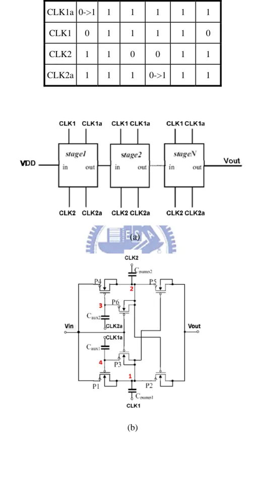
Table 3.3 The clock logic table of the charge pump circuit using PMOS devices. CLK1a 0->1 1 1 1 1 1 CLK1 0 1 1 1 1 0 CLK2 1 1 0 0 1 1 CLK2a 1 1 1 0->1 1 1 (a) (b)
27
(c)
Fig. 3.13 (a) The block diagram of the charge pump circuit using all PMOS devices, (b) The one stage of this charge pump circuit, and (c) its clock waveforms.
3.8.2 The Six-Phase Charge Pump Circuit
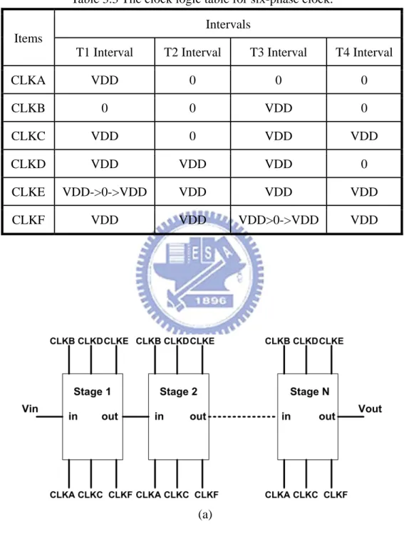
Fig. 3.14 shows the charge pump circuit utilized six-phase clock with four-stage [15]. In Fig. 3.14 (b), it is utilized a voltage level shift in this circuit and has two branched to transfer charge from input to Vout alternately.
At the T1 interval, Ma3 is turn on to let node dr3 become Vin+VDD, Mp3 is turned on to transfer charge to Vout, and other devices are turned off. At this time, the voltage of dr1, dr2, and Net2 are Vin, and dr4 is from Vin to Vin-VDD and then to Vin when CLKE changes from VDD to 0 and the to VDD.
At the T2 interval, Ma3 is still turned on to connect Net 1 and dr3 with the voltage, Vin, and the voltage shift is worked to change the voltage of Ca1 to Vin-VDD as Ma2 is turned on. At the T3 and T4 intervals, the operation is liked to at the T1 and T2 intervals but the difference is the another branch to work, such as Ma4, Mp4, Mp1at T3 interval, and Ma1and Ma4 at T4 interval.
By using this charge pump circuit, it could operate at low-voltage process, because of
(
Vin VDD)
Vtp VDD VtpVin− − > ⇒ > , (3.20) when Ma3 is turned on.
Although these charge pump circuit with all PMOS devices could have better efficiency, but it used much more devices and multi-phase clock to control these circuit. Hence, it can
28
consume extra power at other circuits. In addition, there are larger parasitic capacitors in PMOS than NMOS, and the pumping speed of PMOS charge pump circuits is slower than NMOS.
Table 3.3 The clock logic table for six-phase clock. Items
Intervals
T1 Interval T2 Interval T3 Interval T4 Interval
CLKA VDD 0 0 0 CLKB 0 0 VDD 0 CLKC VDD 0 VDD VDD CLKD VDD VDD VDD 0 CLKE VDD->0->VDD VDD VDD VDD CLKF VDD VDD VDD>0->VDD VDD (a)
29
(b)
(c)
Fig. 3.14 (a) The six-phase charge pump circuit with four-stage, (b) the one stage circuit of this charge pump circuit, and (c) its clock waveforms.
3.9
T
HEC
HARGEP
UMPC
IRCUITW
ITHOUTG
ATEO
XIDER
ELIABILITYI
SSUEDue to the fact that the CMOS technology is continuously scaled down, some modified charge pump circuits based on Dickson charge pump circuit were invented to eliminate the body effect, to overcome the threshold drop, and to improve the efficiency. However, those charge pump circuits are suffered by the gate oxide reliability issue.
Fig. 3.15 shows the charge pump circuit designed with low-voltage devices but without suffering the gate oxide reliability issue because of no overstress voltage across it during the
30
circuit operation [16]. CLK and CLKB are out-of-phase with the amplitude of VDD.
When CLK is low (CLKB is high), mn5 is turned on to transfer charge from VDD to node 5, and mp1 is turned on to transfer charge from node 1 to node 2, the output of the first stage. Furthermore, the voltage of node 1 and node 2 are 2VDD, and node 5 is VDD. At the next half period, CLK is high and CLKB is low, mn1 is turned on to connect input (VDD) and node 1 became to VDD due to the low logic of CLKB, and mp5 is turned on to connect node 5 and output of the first stage, the same with node 2. In the meanwhile, the voltage of node 1 is VDD, node 5 is 2VDD, and the node between of mp5 and mn6 is 2VDD.
This circuit used two branches to avoid the gate oxide reliability, where the voltage difference between the drain/source and the gate in each MOSFET is not over VDD. This circuit has no threshold drop through using switches to transfer charge from input to output. However, in this charge pump circuit, the return-back leakage current during the transition of clocks will cause some degradation on the output voltage (Vout). For example, shown in Fig. 3.16, when CLK from high to low (CLKB from low to high), the voltage of node 1 becomes VDD from 2VDD, the voltage of node 5 becomes 2VDD from VDD, and the voltage of node 2 still holds in 2VDD. Hence, it is expected that mn1 in Fig. 3.15 has to be turned off and simultaneously mp1 in Fig. 3.15 has to be turned on. Actually, mn1 could not be turned off immediately but mp1 was turned on already, so mn1 and mp1 would provide a leakage path such that the voltage at node 2 will return back from 2VDD to VDD through mp1 and mn1 to the input node of VDD.
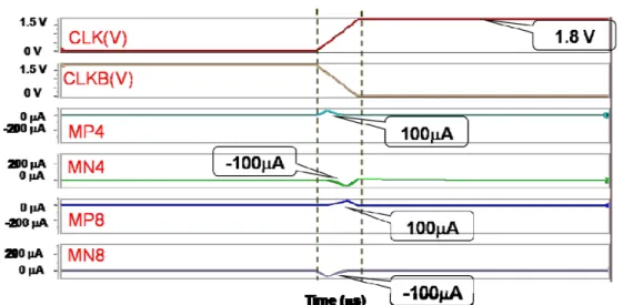
From the simulation of the leakage current in this charge pump circuit, in Fig. 3.17, the leakage current of PMOS is positive current and of NMOS is negative current. Moreover, it is the largest quantity of the leakage current in the last stage, and for this circuit, there are about 100μA to consume the power.
31
Fig. 3.15 The charge pump pump circuit with no gate oxide reliability issue.
Fig. 3.16 The leakage path during the clock transitions.
32
3.10
S
UMMARYBecause the CMOS technology is continuously scaled down, the overstress limitation of the gate oxide has to be overcome. For the supply voltage becomes more and more lower, it has more and more opportunities to use charge pump circuit to generate higher voltage than VDD or lower voltage than GND. Nevertheless, there are more problems produced as the charge pump circuit used due to the process scaling down. From the prior arts, many circuits are used to solve some problems like the body effect, threshold drop, overstress on the gate oxide, and poor efficiency. However, it is serious for the advanced processes that there is a leakage current path in these charge circuits.
33
Chapter 4
The New Proposed Charge Pump Circuit
4.1
I
NTRODUCTIONFor preventing the return-back leakage current, it has the time interval between the clock transitions to alternate the turn-on time of devices. Moreover, it needs more clock signals to control the extra time interval, and the time has to be shorter to avoid the degradation of Vout. Therefore, it needs additional devices and clocks to control the turn-on time of the charge transfer devices in the new proposed charge pump circuit.
4.2
T
HEO
PERATION OFT
HEN
EWP
ROPOSEDC
HARGEP
UMPC
IRCUITThe new charge pump circuit is proposed to suppress the return-back leakage current in the prior-art circuit during clock transitions, and therefore its pumping efficiency can be further improved for implementation in the low-voltage CMOS processes.
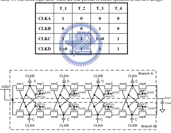
Fig. 4.1 (a) shows the new proposed charge pump circuit with the corresponding clock waveforms shown in Fig. 4.1 (b). The all clock signals (CLKA, CLKB, CLKC, and CLKD) are non-overlapping with the amplitude of VDD. C is the main pumping capacitor, and Cs is the auxiliary pumping capacitor with a small capacitance. With PMOS (mc1, mc2, mc3, mc4, md1, md2, md3, and md4) of small device dimension and the auxiliary Cs capacitors to control the main charge transfer devices (mp1, mp2, mp3, mp4, mp5, mp6, mp7, and mp8) turning off properly, the return-back leakage current during the clock transitions can be avoided. Branch A and Branch B are identical but their turned-on periods are separated in the time domain. Branch A and Branch B are alternately operated to pump output voltage to high.
34
During the Interval T_1
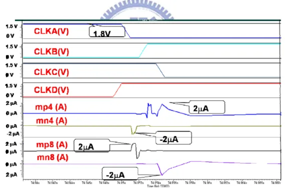
During the interval T_1, CLKA, CLKB, CLKC, and CLKD are high, low, high, and high to low, respectively. At this moment, the voltage difference V15 (V37) between node 1 and node 5 (node 3 and node 7) is –VDD; hence, mn1 and mc1 (mn3 and mc3) are turned on to transfer charge from input node of VDD to node 1 (node 2 to node 3) and transfer charge from node 5 (node 7) to node c1 (c3). At the same moment, mp5 and mn6 (mp7 and mn8) are turned on to transfer charge from node 5 to node 6 (node 7 to node 8). Simultaneously, mn5 (mn7) is kept off to cut off the leakage path from node 5 back to input node of VDD (node 7 back to node 6), and mp1 and mn2 (mp3 and mn4) are kept off to cut off the leakage path from node 2 back to node 1 (node 4 back to node 3).
Hence, for the output stage, mp4 and mn8 are turned on (mn4 and mp8 are kept off,), and the pumping voltage will be transferred from node 4 to the output.
During the Interval T_2 and T_4
During the interval T_2 and T_4, CLKA, CLKB, CLKC, and CLKD are low, low, high, and high, respectively. At this period, the main charge transfer devices ( mn1, mn2, mn3, mn4, mn5, mn6, mn7, and mn8) are turned off because all the voltage difference from gate to source of charge transfer devices are zero. In the meantime, the PMOS (mc1, mc2, mc3, mc4, md1, md2, md3, and md4) of small device sizes are turned on to rise the node c1/d1, c2/d2, c3/d3, and c4/d4 to the voltage level of 2VDD, 3VDD, 4VDD, and 5VDD, respectively. Therefore, the gate voltages of all charge transfer PMOS devices (mp1, mp2, mp3, mp4, mp5, mp6, mp7, and mp8) are higher than their corresponding source voltages to keep themselves off.
During the Interval T_3
During the interval T_3, CLKA, CLKB, CLKC, and CLKD are low, high, high to low, and high, respectively. At this moment, the voltage difference V15 (V37) between node 1 and node 5 (node 3 and node 7) is VDD; hence, mn5 and md1 (mn7 and md3) are turned on to transfer charge from the input node of VDD (node 6) to node 5 (node 7), and transfer charge
35
from node 1 (node 3) to node d1 (d3). At the same moment, mp1 and mn2 (mp3 and mn4) are turned on to transfer charge from node 1 to node 2 (node 3 to node 4). Simultaneously, mn1 (mn3) is kept off to cut off the leakage path from node 1 back to the input node of VDD (node 3 back to node 2), and mp5 and mn6 (mp7 and mn8) are kept off to cut off the leakage path from node 6 back to node 5 (node 8 back to node 7).
Hence, for the output stage, mp8 and mn4 are turned on (mn8 and mp4 are kept off), and the pumping voltage will be transferred from node 8 to the output.
Table 4.1 The clock logic table. There are four periods of circuit operation in this new design.
T_1 T_2 T_3 T_4 CLKA 1 0 0 0 CLKB 0 0 1 0 CLKC 1 1 1->0 1 CLKD 1->0 1 1 1 (a)
36
(b)
Fig. 4.1 (a) New proposed charge pump circuit, and (b) the corresponding clock waveforms.
4.3
S
IMULATEDR
ESULTSA 65-nm CMOS process model with 2.5-V devices is used to simulate and the new proposed charge pump circuit, the prior-art circuit, and Dickson charge pump circuit. To have a fair comparison, the new proposed charge pump circuit and the prior-art circuit of Fig. 3.15 are designed with the same pumping capacitors (C) of 2pF, 4pF for Dickson charge pump circuit, the power supply VDD of 1.8V, the clock frequency of 10MHz, the same size dimensions of charge transfer devices, and the same output loading capacitor of 20pF. Additionally, the auxiliary capacitor (Cs) in the new proposed charge pump circuit is designed with 25fF. Ideally, the output voltage of four-stage charge pump circuit with power supply voltage 1.8V is 9V.
4.3.1 Simulations and Comparisons with the Prior Art [16]
Fig. 4.2 shows the simulated voltage waveform of each node in the new proposed charge pump circuit with four-stage to verify the gate oxide reliability issue, and the output voltage of this work is 8.85V with the supply voltage is 1.8V. Fig. 4.3 shows the leakage current waveforms to compare the result in Fig. 3.17. The simulated output voltage of the new proposed charge pump circuit is 8.85V in Fig. 4.4, the output voltage of prior-art circuit (Fig.
37
3.15) is only 8.28V, and the output voltage of Dickson charge pump circuit is 5.46V, where the rise/fall time of all clock signals is 1ns. In addition, when the rise/fall time of clock signals is increased, the time period of the return-back leakage current will become longer, so the quantity of return-back leakage current will increase during the clock transitions.
To estimate the return-back leakage current, Fig. 4.5 shows the method how to calculate it. For the PMOS, the return-back leakage current is positive. It can be approximately calculated, with its peak value and the time period that the leakage happened, by using the formula of triangle area. Finally, the estimated return charge is the result of adding all leakage currents (all the triangles) during the same period of clock transition. Similarly, for the NMOS, the return-back leakage current is negative, and the estimated method is the same as that with PMOS. The estimation result of return charge is shown in Fig. 4.6 under the clock signals with different rise/fall time. From this simulated/estimated results, the new proposed charge pump circuit has much smaller leakage current than that in the prior-art circuit of Fig. 3.15. In Fig. 4.7, when the rise/fall time of clock signals is increased, the time period of return current happened is also increased, and therefore the output voltage of the prior-art circuit is significantly decreased. However, by using this new proposed design, the degradation on the output voltage of charge pump circuit due to the long rise/fall time in the clock transition can be rescued.
38
Fig. 4.2 The simulated voltage waveforms at the nodes 1~8 and the output (Vout) in the new proposed charge pump circuit with VDD of 1.8V.
39
Fig. 4.4 The variations of the output voltages with different output loading.
Fig. 4.5 The method used to estimate the return charge during the clock transition in the charge pump circuit. In this figure, two cases with rise/fall time of 1ns and 12 ns are
40
Fig. 4.6 The estimated return charge of the charge pump circuits under with different rise/fall time in the clock signals (f=10MHz, VDD=1.8V).
Fig. 4.7 The simulated output voltage of the charge pump circuits under with different rise/fall time in the clock signals (f=10MHz, VDD=1.8V).
41
4.3.2 Simulation of the Efficiency
Efficiency is a main point to test how better the charge pump circuit is, and the power consumption is relative with the efficiency [17]. The calculate the efficiency rule is
DD power out L V I V I (%) Efficiency • • = , (4.1) where
(
)
L s power N I I I = +1 • + (4.2) and DD p s N C f V I = • • • . (4.3)From Fig. 4.8 (a) and (b), they show why the reason of the input current is N+1 times of the output current. At the transient time, the charges from input are transfer to the output in every period and become more from the clock providing, so the charges will be transferred from stage by stage and enhanced by clock signals. When it is operated at the steady state, the output stage is exported 5Q in every period for the example in Fig. 4.8 (a). Fig. 4.8 (b) shows the voltage waveform of some pumping node of a charge pump circuit, the voltage drop is the result of that the leakage current flows to the parasitic capacitors after this node is pumped highly. Therefore, the total input current is (a) + (b) when a charge pump circuit is working.
42
(a)
(b)
Fig. 4.8 (a) The steps of the charges are transferred during the clock period, and (b) it is the voltage waveform of a pumping node in a charge pump circuit.
4.3.3 Simulations for Different VDD
For the 2.5-V process, Fig. 4.9 shows the efficiency in different VDD. The efficiency of this work (the new proposed charge pump circuit) is upper than 80% in any supply voltage. The efficiency of the prior art circuit is lower than the efficiency of this work, but it has a little rising tendency because of the less leakage current produced in the low supply VDD. Fig.
43
4.10 shows the output ripples in different VDD, and the ripple is 100 (%)= •
Vout V
Ripple pp , (4.1)
where Vpp is the peak-to-peak value of Vout. Since this work can reduce the leakage current,
the ripple of this work is smaller than the prior art circuit. For VDD=3V, the ripple of this work is 0.27% and the prior art circuit is 0.96 %. For VDD=1V, the ripple of this work is 0.006% and the prior art circuit is 0.09 %. If the ripple is small enough, the output is more suitable to connect with other circuit which needs the higher voltage (lower voltage). And in Fig. 4.11, for VDD=3V, the output voltage of this work is 14V and the prior art circuit is 13.3V. For VDD=1V, the output voltage of this work is 4.94V and the prior art circuit is 4.91V. Therefore, this work can operate in low supply voltage and apply in low-voltage process.
Fig. 4.9 The efficiencies of this work and the prior art circuit are in different supply voltages VDD with the 1MegΩ loading resistance.
44
Fig. 4.10 The output ripples of this work and prior art circuit are in different supply voltages VDD and without loading resistance (Rout).
Fig. 4.11 The output voltage decreases when the supply voltages are decreasing and without loading resistance (Rout).
45
Chapter 5
Measured Results of the New Proposed
Charge Pump Circuit
A test chip has been fabricated in a 65-nm CMOS process with 2.5-V device to verify the new proposed charge pump circuit and the prior-art circuit (Fig. 3.15). Each size of devices in these charge pump circuits is show in Table 5.1. The chip photograph, which contains Bulk (twin-well process) and DNW (deep n-well process), is shown in Fig. 5.1, the chip sizes are 350μm*415μm for the prior art and 385μm*440μm for the new proposed charge pump circuit.
Table 5.1 For the fair comparison, each size of all devices have to the same in different charge pump circuits.
Prior art [16] This work
PMOS (μm/μm) 8/0.28 8/0.28 NMOS (μm/μm) 4/0.18 4/0.28 PMOSsmall (μm/μm) 0 0.4/2 Cpump (pF) 2 2 Csmall (fF) 0 25 Cout (pF) 20 20 CLK 2 4 VDD (V) 1.8 1.8 Frequency (MHz) 10 10 Stage number 4 4
46
(a)
(b)
Fig. 5.1 (a) The chip photograph about Bulk and DNW for the prior art circuit, and (b) the new proposed charge pump circuit, fabricated in a 65-nm CMOS process.
5.1
T
HEP
RIORA
RTC
IRCUIT[16]
The charge pump circuit of the prior art needs two clock signals, one input, and one output, so the measurement setup is shown in Fig. 5.2. The power supply is connected to the
47
input of the chip, clock generator is connected to the clock input of the chip, and the output of this chip is connected to the scope to observe the output waveforms in different resistors. The clock signals of this prior art is measured to shown in Fig, 5.3, with frequency is10MHz, amplitudes are 1.8V, and the rise/fall time is 2ns. The measurement result is shown in Fig. 5.4. Additionally, the output voltage is 7.96V for the bulk process and 8V for the DNW process. Fig. 5.5 shows the measurement results of each chip of the prior art with the bulk process and DNW process. Finally, it shows the average measured outputs compared with the simulated results in Fig. 5.6. The output voltages without loading are 8.28V for simulation, 7.84V for the bulk process, and 7.98V for DNW process. For different supply voltage shown in Fig. 5.7, the highest supply voltage of the prior art circuit in bulk process is only at 1.8V, because the breakdown voltage of this prior art circuit is about 10V. From this measured result, the output voltage in DNW process is similar to the result of the simulation. Hence, the simulation result of the prior art circuit is 9.98V and the output voltage in DNW process is 9.88V for VDD=2.2V. The output voltage in the bulk process is 7.8V in the bulk process.
48
Fig. 5.3 The clock waveforms of the prior art circuit.
49
(a)
(b)
50
Fig. 5.6 The average output voltages about the prior art circuit with bulk process, DNW process, and simulation.
Fig. 5.7 The output voltages in different supply voltages VDD and without loading resistance (Rout).
![Fig. 2.2 It is Cockcroft-Walton voltage multiplier, and s, t, x, y, and z are the input impedances from their nodes [2]](https://thumb-ap.123doks.com/thumbv2/9libinfo/8144037.166784/17.892.169.772.115.311/fig-cockcroft-walton-voltage-multiplier-input-impedances-nodes.webp)