國 立 交 通 大 學
電子工程學系 電子研究所碩士班
碩 士 論 文
利用 RTS 方法研究 SONOS 快閃記憶體
寫入/抹除電荷之橫向分佈特性
Characterization of Program/Erase Charge Lateral
Distribution in SONOS Flash Memory Cell by Using
RTS Technique
研 究 生 :趙元鵬
指導教授 :汪大暉 博士
中華民國 九十七 年 六 月
利用 RTS 方法研究 SONOS 快閃記憶體寫入/抹除
電荷之橫向分佈特性
Characterization of Program/Erase Charge Lateral
Distribution in SONOS Flash Memory Cell by Using
RTS Technique
研 究 生 :趙元鵬 Student : Yuan-Peng Chao
指導教授 : 汪大暉 博士 Advisor : Dr. Tahui Wang
國立交通大學
電子工程學系 電子研究所碩士班
碩士論文
A Thesis
Submitted to Department of Electronics Engineering & Institute of Electronics
College of Electrical and Computer Engineering
National Chiao Tung University
In Partial Fulfillment of the Requirements
For the Degree of Master
In
Electronic Engineering
June 2008
Hsinchu, Taiwan, Republic of China.
i
利用 RTS 方法研究 SONOS 快閃記憶體
寫入/抹除電荷之橫向分佈特性
學生:趙元鵬
指導教授:汪大暉 博士
國立交通大學 電子工程學系 電子研究所
摘要
本篇論文主要提供了一個新的方法來探測小面積 SONOS 快閃記憶體沿著通 道的表面電位變化,這個新方法是藉由結合缺陷位置萃取技術和底層二氧化矽缺 陷所產生的隨機電報雜訊(Random Telegraph Noise)來達成。我們使用這個新方法來驗證 SONOS 快閃記憶體中通道熱電子(Channel Hot Electron)的寫入電荷分佈和通道引發二次電子射入的電荷分佈之不同。此外,這 個 方 法 也 被 應 用 在 觀 察 通 道 熱 電 子 寫 入 和 能 帶 到 能 帶 穿 隧 產 生 之 熱 電 動 (Band-to-Band Tunneling Hot Hole)抹除電荷分佈的不對稱現象。最後,高溫下氮 化矽中的正電荷遷移也有利用此方法研究。
ii
Characterization of Program/Erase Charge Lateral
Distribution in SONOS Flash Memory Cell by Using
RTS Technique
Student: Yuan-Peng Chao Advisor: Dr. Tahui Wang
Department of Electronics Engineering &
Institute of Electronics
National Chiao Tung University
Abstract.
The main concept of this dissertation provides a new method to probe the change of the surface potential along the channel in a small area SONOS type memory. It is accomplished by combining the extraction of the trap position with the random telegraph signal (RTS) resulted from the interface trap located in the bottom oxide. This method is used to verify the difference of the program charge distribution between channel hot electron (CHE) and channel initiated secondary electron (CHISEL) injection. Moreover, this method could be applied to observe the charge misalignment of CHE program and band-to-band tunneling
iii
(BTBT) hot hole erase. The migration of the positive charge in the nitride layer is also inspected as well.
iv
謝誌
本篇論文完成,首先要感謝指導教授汪大暉教授。汪大暉教授提供了良好的 實驗儀器及研究環境,使我們可以進行許多先進元件的研究。他紮實且深入的研 究訓練,加上嚴謹的研究態度,讓我獲益良多。 再來最需要感謝的就是指導我實驗的馬煥淇學長。在實驗做不出來的時候, 給我明確的方向,也教了我做實驗的方法與態度。另外還要感謝實驗室的小鄭、 DaDa、阿雄和阿多肯學長給予我生活上和學業上的意見,在我剛進實驗室時,幫 助我融入這個實驗室。同屆的彥君、佑亮、小熊、還有子華,感謝他們在我失意 的時候,都能在我身邊給予我精神上的支持。最後還有學妹阿杜和莊 group 的同 學們,讓我的研究生生活,除了嚴肅的學術研究外,還多了許多歡樂。 最後要感謝我的父母、家人,在求學期間給我的鼓勵和支持,有了他們經濟 上支持,無怨無悔的付出與關心,才能讓我完成我的碩士學位。 2008.4v
Contents
Chinese Abstract
iEnglish Abstract
iiAcknowledgement
ivContents
vFigure Captions
viChapter 1
Introduction
1Chapter 2
Random Telegraph Signal Mechanism and
Trap Position Extraction
2
2.1 Introduction 2
2.2 RTS Theory 2
2.3 How to Use RTS Noise 3
2.4 Measurement of RTS Noise 4
2.5 Extraction of The Trap Position 5
Chapter 3
Inspection of Programmed Charge Lateral
Distribution in SONOS Flash Memory Cell
by Using RTS Technique
15
3.1 Introduction 15
3.2 Device Structure and Programming Conditions 16 3.3 Surface Potential Change during CHE
Programming
16 3.4 Comparison of CHE and CHISEL Programming 17
Chapter 4
Other Application Utilizing Individual
Traps as Internal Probes
26
4.1 Introduction 26
4.2 CHE Program and BTBT Hot Hole Charge Misalignment
26
4.3 Hole Lateral Migration 27
Chapter 5
Conclusions
40vi
Figure Captions
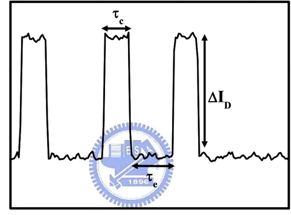
Fig. 2.1 Typical time domain plot of the drain current of RTS noise. Illustration of the three major parameters of RTS noise.
p.7
Fig. 2.1 Typical time domain plot of the drain current of RTS noise. Illustration of the three major parameters of RTS noise.
p.8
Fig. 2.3 The experimental setup for measuring RTS p.9 Fig. 2.4 RTN corresponding to different gate voltage p.10 Fig. 2.5 Extracted capture time (τc) vs. gate voltage p.11
Fig. 2.6 Correlation of capture time and Vg at different drain voltage p.12 Fig. 2.7 Illustration of the objects meaning in trap position extraction p.13 Fig. 2.8 Another example of the extraction of the trap position p.14 Fig. 3.1 The trap position along the channel p.19 Fig. 3.2 The capture time and emission time after programming. The measuring
condition is Vg = 6V, Vd = 0.1V.
p.20
Fig. 3.3 The variation of capture time over emission time after programming p.21 Fig. 3.4 The change of surface potential after programming p.22 Fig. 3.5 Capture time after programming at different side p.23 Fig. 3.6 Illustration of CHE and CHISEL mechanisms p.24 Fig. 3.7 The variation of capture time after programming by CHE and CHISEL p.25
Fig. 4.1 The charge distribution of CHE program and BTBT hot hole erase. The distribution of electrons is wider than the distribution of holes.
p.30
Fig. 4.2(a)The position extraction of one of the trap used in misalignment experiment.
p.31
Fig. 4.2(b)The prediction of the surface potential variation during program and erase
p.31
vii
experiment.
Fig. 4.3(b)The prediction of the surface potential variation during program and erase p.32 Fig. 4.4 The relative energy of the trap at 0.3L from the drain during program and
erase. ΔEt is not reversible in this case.
p.33
Fig. 4.5 The variation of the relative energy of the trap at 0.05L from the drain side. ΔEt is reversible in this case.
p.34
Fig. 4.6(a)The extraction of the trap position used in hole migration experiment p.35 Fig. 4.6(b)The hole distribution and band diagram before and after heating p.35 Fig. 4.7 The variation of trap relative energy while heating p.36 Fig. 4.8(a)The extraction of the trap position used in hole migration experiment p.37 Fig. 4.8(b)The hole distribution and band diagram before and after heating p.37 Fig. 4.9 The variation of the trap relative energy while heating p.38 Fig. 4.10 The surface potential change under high temperature after programmed by
CHE at the source side
1
Chapter I
Introduction
Nowadays, flash memories are widely used in personal computers and electronic products. Due to the non-volatile property, the data can be stored, erased and read from the devices for many times and the data will not be lost after the power is off. Nevertheless, with recent advances in VLSI processing, we have reached the point at which the effect of a single electron on a typical device can be quite significant. While such effects will eventually cause fundamental scaling and reliability problems, parallel advances in physics have helped create opportunities for extracting new kinds of information about VLSI devices by observing single-electron trapping effects. In this thesis, channel hot electron (CHE) is used to program the memory cell, and with the random telegraph signal (RTS) resulted from the interface trap in the bottom oxide[1.1][1.2], the surface potential variation in the vicinity of the trap could be investigated during programming. Next, accompanied with the trap position extraction technique[1.3], the surface potential change can be known at a specific position along the channel. Besides, this method may also be utilized to observe the channel surface potential change of the devices in other applications.
There are five chapters in this thesis. Chapter 1 is Introduction and we would give a brief outline of the dissertation. In Chapter 2, the RTS mechanism is reviewed and the trap position extraction idea will be explained. In Chapter 3, the experimental process and result of probing the channel surface potential throughout CHE programming will be described, and next, other applications will be shown in Chapter4. Finally, the summary and conclusion will be given in Chapter5.
2
Chapter 2
Random Telegraph Signal Mechanism and
Trap Position Extraction
2.1 Introduction
Trapping of a single carrier charge in defect states near the Si/gate dielectric interface and related local modulation in carrier density and mobility will have a profound effect on the drain current in such devices. Current fluctuations on such a scale will become a serious issue, not only as a source of excessive low-frequency noise in analog and mixed-mode circuits, but also in dynamic random access memory and static random access memory and other digital application.
Depending on the device geometry, a single or few discrete charges trapped in hot carrier, radiation or bias temperature stress created defect states will be sufficient to cause significant performance degradation in nanometer scale SONOS flash memories. For devices with very small channel area, it is possible to have only one oxide trap in the vicinity of surface Fermi level over the entire channel. Thus, individual traps can be observed in their neutral or charged state and the current fluctuation between two discrete levels. The study of random telegraph signal (RTS) noise in submicron MOS transistors offers the unique opportunity of studying the trapping/de-trapping behavior of a single interface trap.
2.2 RTS Theory
Fig. 2.1 displays a typical time domain trace of the drain current illustrating the three main RTS parameters. In small enough devices, normally, only trap energy level
3
within a few kT from the Fermi level would make current fluctuation where k and T are the Boltzmann’s constant and equilibrium temperature, respectively. Traps with energy levels several kT below the Fermi level would be permanently filled while traps with energy levels several kT above the Fermi level would be permanently empty, resulting in negligible noise power.
Up to now, the discrete change in current has generally been modeled as the superposition of two effects that occurs when the trap changes its state: the effect of number fluctuation of free channel carriers ΔN, and the mobility fluctuation Δμ described as [2.1][2.2]:
Eq (2.1)
in strong inversion. Here, N is the channel carriers per unit area. It is assumed that the mobility is limited by oxide charge scattering with a coefficient α. The sign in front of the mobility fluctuation is determined by the type of the trap, i.e., a repulsive or an attractive scattering center. For an acceptor trap, the high level corresponds to the trap in a neutral state while the low level corresponds to the negatively charged state. Therefore, the RTS are completely determined by the up and down times and its amplitude.
2-3 How to Use RTS Noise
RTS noise is characterized by three parameters: the average of the high (<τc>)
and low (<τe>) time constants and the magnitude of the current fluctuation (∆Id),
which are also shown in Fig 2.1. The range of the time constants is from mili-seconds to seconds. Since there is an important relation between <τc>/<τe> and Et-EF:
1 1 [ ] d d I N I N W L N μ αμ μ Δ = Δ ±Δ = − ± ⋅
4
Eq (2.2)
where g is the degeneracy factor, Et-EF is the trap energy relative to the Fermi-level,
and the trap is at the interface of the bottom oxide, we could use <τc>/<τe> to
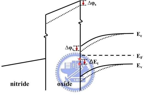
inspect the surface potential change as shown in Fig. 2.2.
2-4 Measurement of RTS Noise
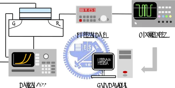
Agilent-4155C was used for our measurements of small-area SONOS at room temperature. The sampling mode was selected, and the bias voltages (VD, VG) were well controlled so that the traps were kept in the vicinity of the Fermi level. With fast enough sampling rate, the current fluctuation would be extracted and shown on the screen of 4155C.
A program written by Fortran 6.0 was used to extract the capture time (τc) and
the emission time (τe), which used the numbers of the points in the data from 4155C
and the interval of any two points to compute the time constants. The whole measurement setup is shown in Fig. 2.3.
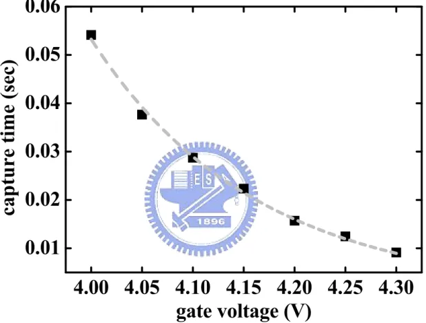
The capture time is sensitive to the concentration of the carriers in the channel under the trap, which is described as [2.3]
Eq (2.3)
where n is the electron density in the channel under the trap, σ is the capture cross-section, and vth is the thermal velocity. Therefore, as shown in Fig. 2.4 and Fig.
2.5, with the gate voltage increased, the capture time would be decreased due to the increased carrier concentration below the trap.
1 c th n v τ σ = exp( ) c t F e E E g kT τ τ < > − = < >
5
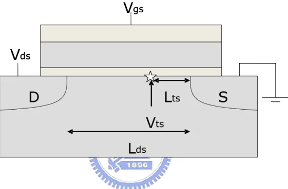
2-4 Extraction of the Trap Position
Before RTN is utilized to detect the potential variation in the channel, an important element is to find the location of the trap in the device. The method was proposed by IBM[1.3] which is based on the characteristic of linear voltage drop along the channel while operated in linear region. Thus, the applied drain voltage (Vds)
affects the trap in a manner which depends on its position in the device. The experimental detail is described as below.
The devices used here are SONOS flash memories with a top oxide of 7nm, a nitride layer of 8.5nm and a bottom oxide of 6nm. The channel length (L) is 0.1μm, and the channel width (W) is 0.1μm.
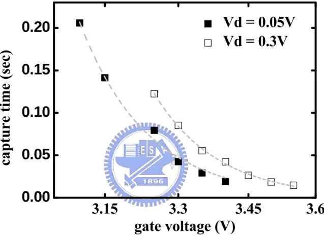
First, a very small voltage is given (0.05V),which could almost be neglected, to the drain side, and the correlation between the capture time (τc) and gate voltage (Vg)
is measured, which is plotted in Fig. 2.6. Next, the drain voltage is increased to 0.3V also with the relation of capture time and Vg measured, and the result is shown in Fig.
2.6 as well. Note that the operations are all in the linear region. Since the capture time (τc) is dominated by the voltage drop between the gate and the channel right below
the trap, the amount of the lateral shift of these two curves is equal to the voltage raised by the drain side at the point of the trap. Therefore, the following equation allows us to extract the trap position along the channel:
Eq (2.4)
where Vts denotes the voltage raised at the trap position by the drain voltage and other
meanings of the objects are specified individually in Fig. 2.7. For this case, the trap is at the position of 0.2L to the source side, where L is the channel length. Another
ts ts ds ds
V L
=
6
7
τ
cΔ
I
DI
Dtime
τ
eτ
cΔ
I
DI
Dtime
τ
eFig. 2.1 Typical time domain plot of the drain current for RTS noise. Illustration of the three major parameters of RTS noise.
8
∆φ
sE
cE
vE
F∆φ
s∆E
toxide
nitride
Fig. 2.2 The band diagram showing the energy change of the trap and the surface potential <τc>/<τe> can be used to investigate ∆Et and therefore ∆ψs
9
Agilent 4155
Current Amp. Oscilloscope
Data Analysis
D S
Fortran 6.0 Program
1.E+5
10
0.0
0.5
1.0
1.7
1.8
1.9
2.0
Vg = 3.10 Vg = 3.20 Vg = 3.30 Vg = 3.40Id
(
μ
A
)
time (sec)
Fig. 2.4 RTN corresponding to different gate voltage. A larger Vg makes the capture time (τc) shorter.
11
4.00 4.05 4.10 4.15 4.20 4.25 4.30
0.01
0.02
0.03
0.04
0.05
0.06
cap
tu
re time (sec)
gate voltage (V)
12
3.15
3.3
3.45
3.6
0.00
0.05
0.10
0.15
0.20
cap
ture t
ime (s
ec)
gate voltage (V)
Vd = 0.05V
Vd = 0.3V
13
Fig. 2.7 Illustration of the objects meaning in trap position extraction
V
gsD
S
V
dsV
tsL
tsL
dsV
gsD
S
V
dsV
tsL
tsL
ds14
1.9
2.0
2.1
2.2
2.3
0.03
0.06
0.09
0.12
τ
c
(sec)
V
g
(V)
Vd = 0.05V
Vd = 0.3V
≈ 0.28V
0.07L
D
S
15
Chapter 3
Inspection of Programmed Charge Lateral Distribution in
SONOS Flash Memory Cell by Using RTS technique
3-1 Introduction
In two-bit operation, the control of programmed charge lateral distribution of each bit is a major concern for the scalability of the SONOS cell. Attempts have been made in the past to characterize the trapped charge distribution in a SONOS cell[3.1][3.2]. An inverse modeling approach is applied to extract programmed charge distribution from measured I-V curves [3.1]. This method has some drawbacks, such as lack of precise device doping and extensive numerical calculation. Charge pumping has been used widely to profile the charge distribution in a MOSFET device [3.3][3.4]. A modified charge pumping technique [3.5] is proposed to probe the lateral distribution of programmed charges at the source and drain junctions separately without computer simulation. However, when it comes to an ultra-small device, this method is not able to be utilized due to the ultra-small charge pumping current which could not be detected by the experimental instruments. Whereas RTN is very sensitive to the potential change around the trap, it provides an opportunity to make this mechanism useful to detect the surface potential variation throughout programming. The devices and measurement setup throughout this study will be described. The position of the trap along the channel will be extracted. The inspection of the channel surface potential change at a specific position will be demonstrated by this RTN method.
16
3-2 Devices Structure and Programming Conditions
The devices in our experiment are SONOS flash memories with a top oxide of 8.5nm, a nitride layer of 7nm, a bottom oxide of 6nm, a gate length of 0.1μm and a gate width of 0.1μm. The gate and drain voltages are 8V and 3.7V respectively during CHE programming with source and bulk grounded.
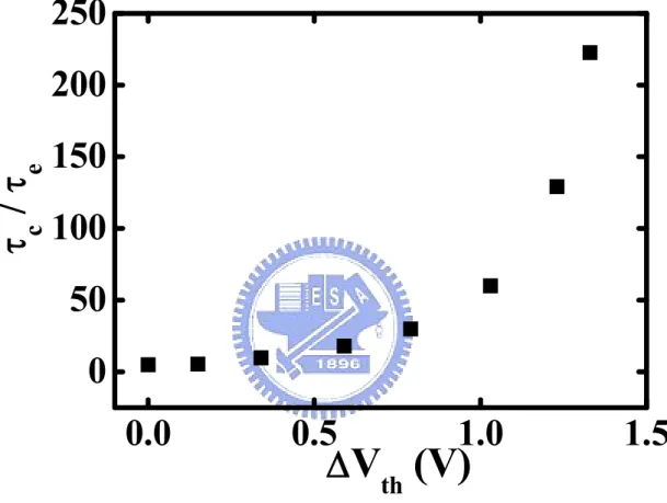
3-3 Surface Potential Change during CHE Programming
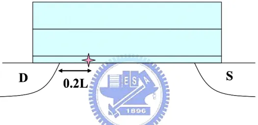
In order to detect one side of the surface potential change during CHE programming in a SONOS flash memory, the trap is needed to be located near the junction so that the program charge could be sensed by the trap. We conducted RTS measurement across the whole wafer and found few RTS events for later use. The trap we used is estimated to be at the position of 0.2L from the drain side where L is the channel length as plotted in Fig. 3.1. Due to the fact that the capture time is related to the electron density under the trap and the emission time is sensitive to the electric potential at the trap location owing to the average vertical electric field in the oxide [3.6][3.7]:
Eq (3.1)
Eq (3.2)
where Nc is the effective density of states in the conduction band and ∆ECT refers to
the additional energy required to move the electron from the trap to the conduction band, it could be predicted that the capture time would increase and the emission time would decrease during the programming process. Our result is shown in Fig. 3.2,
exp( CT) e c E vN kT τ σ Δ 1 < > = c vn τ 1 < > = σ
17
which is quite similar to our prediction. Fig. 3.3 shows the variation of the capture time over the emission time (τc/τe) during programming in which a conversion can
be made into the surface potential change (ΔEt) by Eq (3.3)[3.8] as shown in Fig. 3.4:
Eq (3.3)
where Et – EF represents the trap energy relative to the Fermi level and g is the
degeneracy factor which is equal to one in our case.
The other side has also been programmed, the source side in this case, to make a double confirmation that the trap is indeed located near the drain side. The result is shown in Fig. 3.5. It could be seen that the capture time remains almost constant during programming, and therefore, the trap is not affected by the program charge at the source side.
3-4 Comparison of CHE and CHISEL Programming
The program charge distribution in a flash cell is a crucial issue for two-bit operation scheme. It has been indicated in the previous simulations that the distribution of the program charge by channel initiated secondary electron (CHISEL) injection is different from CHE [3.9][3.10]. Therefore, utilizing our RTS method to observe the surface potential during programming by CHISEL has also been demonstrated as a comparison with the case programmed by CHE.
Each mechanism is illustrated in Fig. 3.6. It could be seen that the hole generated at the first impact ionization will flow to the bulk and results in a secondary impact ionization. The electron from the secondary impact ionization, accordingly, would be accelerated by the minus bulk voltage and be injected into the nitride layer.
exp( ) c T F e E E g kT τ τ − =
18
It was reported that a wider program charge distribution is observed in CHISEL mechanism and the way of CHE has a narrower distribution [3.11] as shown in Fig. 3.6. Thus, it can be predicted that the capture time would be raised more rapidly in CHISEL than in CHE programming method if the trap is assumed to be not too close to the junction. The trap in this case is at the position of 0.2L from the drain side, which is located at a little distance from the junction.
The programming condition of CHISEL is 4V to the gate, 3.3V to the drain, -2V to the bulk with source grounded, and the device we used is the same as the one in CHE experiment previously. The results are shown in Fig. 3.7, and it could be seen that the capture time over the emission time certainly increases more quickly as programmed by CHISEL than CHE. Consequently, the difference of program charge distribution between CHE and CHISEL is verified again with our RTS method.
19
D
0.2L
S
D
0.2L
S
20
0.0
0.3
0.6
0.9
1.2
1.5
0.0
0.1
0.2
0.3
τ
c
(sec)
τ
e
(sec)
τ
cτ
eΔ
V
th
0.001
0.002
0.003
0.004
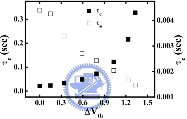
Fig. 3.2 The capture time and emission time after programming The measuring condition is Vg = 6V, Vd = 0.1V.
21
0.0
0.5
1.0
1.5
0
50
100
150
200
250
τ
c
/
τ
e
Δ
V
th
(V)
22
E
cE
fE
tE
t’
99meV
source
drain
0.0
0.5
1.0
1.5
0.00
0.05
0.10
Δ
E
t
(eV)
Δ
V
th
(V)
23
0.0
0.3
0.6
0.9
1.2
1.5
0.0
0.1
0.2
0.3
0.4
Prog. @ S
Prog. @ D
τ
c
(sec)
Δ
V
th
(V)
24
V
dD
S
V
gV
dD
S
-V
BV
gCHE
CHISEL
V
dD
S
V
gV
dD
S
-V
BV
gV
dD
S
-V
BV
gCHE
CHE
CHISEL
CHISEL
25
0.0
0.2
0.4
0.6
0.8
1.0
1.2
0
20
40
60
80
100
τ
c
/
τ
e
Δ
V
th
(V)
CHE
CHISEL
26
Chapter 4
Other Applications Utilizing Individual Traps as
Internal Probes
4-1 Introduction
Inasmuch as the trap is very sensitive to the change of local potential, it could be applied to detect the surface potential variation at a specific position along the channel. In this chapter, two other applications with our method employed are introduced. One is the observation of the charge misalignment between CHE program and band-to-band-tunnel (BTBT) hot hole erase, and the other is the investigation of the hole lateral migration under high temperature.
4-2 CHE Program & BTBT Hot Hole Erase Charge
Misalignment
In SONOS flash memories, the misalignment between program and erase charge has been studied for the last few years, which could lead to a reliability issue as charge accumulating around the junction [4.1]. No matter using the charge pumping or the Monte Carlo simulation method, it has been indicated in previous works that BTBT hot hole erase has a narrower charge distribution, i.e., closer to the junction, and the distribution of CHE program is wider as depicted in Fig. 4.1.
The devices in our experiment are SONOS flash memories with a top oxide of 85A, a nitride layer of 70A, a bottom oxide of 60A, a gate length of 0.1μm and a gate width of 0.1μm. The programming condition is the same as before which is 8V
27
to the gate, 3.7V to the drain with source and bulk grounded. The condition for BTBT hot hole erase is chosen to be -4V to the gate, 5V to the drain with source and bulk grounded.
Utilizing the trap position extraction technique, the locations of the traps used in this experiment are shown in Fig. 4.2(a) and Fig. 4.3(a), which are at the position of 0.3L and 0.05L from the drain side respectively. Since the charge injected by BTBT hot hole erase has a narrower distribution, it could be predicted that only the region in the vicinity of the junction could be affected by the injected charge. Therefore, as a result, the potential change induced by the injected charge could only sensed by the trap at the position of 0.05L from the drain side. On the contrary, the program charge injected by CHE with a wider distribution could affect the area further from the junction, and thus, the potential change could be sensed by both two traps at different positions as shown in Fig. 4.2(b) and Fig. 4.3(b).
Fig. 4.4 and Fig. 4.5 show the shift of the trap relative energy (∆Et) of the two
traps during program and erase. It could be seen clearly that both the program and erase charge are sensed by the trap closer to the junction (0.05L to the drain side). However, only the program charge was sensed by the trap at a further position from the junction (0.3L from the drain side). Therefore a wider charge distribution of CHE program is verified again.
4-3 Hole Lateral Migration
The negative threshold voltage (Vt) shift of a nitride storage flash memory cell in
the erase state will result in an increase in leakage current. By utilizing a charge pumping method, it has been reported that the lateral migration of trapped holes is responsible for this Vt shift due to the channel shortening[4.2]. Also the temperature
28
dependence of the hole migration has been pointed out. In this section, the lateral movement of the positive charges will be monitored by our RTN method through the surface potential variation sensed by the trap.
In Fig. 4.6(a), the trap position is extracted by the method proposed in Chapter 2, which is at the position of 0.1L from the drain side. Since the trap is quite close to the junction, it is expected that the potential change would be sensed immediately by the trap as the holes are injected into the nitride layer as shown in Fig. 4.6(b). Accompanied with the heating time, the lateral migration of the holes will result in a less effect of positive charge on the trap as in Fig. 4.6(b) as well. Therefore the relative trap energy is predicted to be increased because of the less positive charge right above the trap.
The devices we used in this experiment are SONOS flash memories with a top oxide of 8nm, a nitride layer of 6nm, a bottom oxide of 3nm, a gate length of 0.1μm and a gate width of 0.065μm. The erase condition is a gate voltage of -5V and a drain voltage of 4V with source and bulk grounded for 30 millisecond. The temperature is controlled to be under 85°C.
The results are shown in Fig. 4.7, and we could see that the relative trap energy (ΔEt) increases with the heating time which is in agreement with what we have
predicted. It is also noted that ΔEt changes quickly at the beginning and becomes
stable after about 10 minutes which indicates that the holes move fast at the very start but almost stop migrating in the end.
Another case is shown in Fig. 4.8(a) in which the trap is at a longer distance from the junction (0.25L). We could first predict that there would be a different outcome of this situation based on Fig. 4.8(b). The result is depicted in Fig. 4.9, and the surface potential decreases instead of increasing as the former case.
29
30
Drain
Drain
D
S
CHE prog.
BTBT hot
hole erase
Drain
Drain
D
S
CHE prog.
BTBT hot
hole erase
Fig. 4.1 The charge distribution of CHE program and BTBT hot hole erase The distribution of electrons is wider than the distribution of holes.
31
0.3L
D
S
0.3L
D
S
Fig. 4.2(a) The position of the trap used in charge misalignment
E
cE
fE
tE
t’
E
cE
fE
tE
t’’
Drain
Drain
E
vE
v32
0.05L
S
D
0.05L
S
D
Fig. 4.3(a) The position of the other trap used in the experiment
Drain
Drain
E
cE
fE
tE
t’
E
tE
cE
fE
t’’
E
t’
E
vE
v33
1.6
1.8
2.0
2.2
0.00
0.02
0.04
Δ
E
t
(eV)
V
th
(V)
prog.
erase
1.6
1.8
2.0
2.2
0.00
0.02
0.04
Δ
E
t
(eV)
V
th
(V)
prog.
erase
Fig. 4.4 The relative energy of the trap at 0.3L from the drain during program and erase ΔEt is not reversible in this case.
34
1.50
1.65
1.80
0.00
0.05
0.10
0.15
Δ
E
t
(eV)
V
th
(V)
prog.
erase
Fig. 4.5 The variation of the relative energy of the trap at 0.05L from the drain side ΔEt is reversible in this case.
35
Fig. 4.6(a) The extraction of the trap position used in hole migration experiment
E
cE
fheated
Drain DrainE
c EfE
tE
tE
t’
E
vE
vE
cE
fheated
Drain DrainE
c EfE
tE
tE
t’
E
vE
vFig. 4.6(b) The hole distribution and band diagram before and after heating
D S
36
0
10
20
30
40
0.00
0.01
0.02
0.03
0.04
Δ
E
t(eV)
Heating Time (min)
Fig. 4.7 The variation of trap relative energy while heating
37
Fig. 4.8(a) The extraction of the trap position used in hole migration experiment
heated
Drain DrainE
c EfE
tE
cE
fE
tE
t’
E
vE
vheated
Drain DrainE
c EfE
tE
cE
fE
tE
t’
E
vE
vFig. 4.8(b) The hole distribution and band diagram before and after heating
D S
38
0
10
20
30
40
-0.04
-0.03
-0.02
-0.01
0.00
Δ
E
t
(eV)
Heating time (min)
Fig. 4.9 The variation of trap relative energy while heating ΔEt shows a different trend from the former one.
39
0
10
20
30
40
-0.02
-0.01
0.00
0.01
0.02
Δ
E
t(e
V)
Heating time (min)
Fig. 4.10 The surface potential change under high temperature after programmed by CHE at the source side
40
Chapter 5
Conclusion
The study has used oxide interface traps as potential probes to detect the surface potential variation. With the trap position extraction technique, the surface potential change at a specific position could be inspected during CHE program. The comparison of CHE and CHISEL indicates that the charge distribution of CHISEL is wider than CHE.
With appropriate trap positions along the channel, the charge misalignment of CHE program and BTBT hot hole erase was also investigated utilizing our method. It is verified again that the charge distribution of BTBT hot hole erase is narrower than CHE. Besides, we have observed the surface potential variation during hole lateral migration in the nitride layer under high temperature.
Due to the sensitivity of RTN to the potential change around the trap, our method is suitable for inspecting the surface potential change throughout the standard operations. Nevertheless, more applications are needed at the present time.
41
Reference
Chapter 1
[1.1] Ming-Horn Tsai, Hirotaka Muto, and T. P. Ma, “Random telegraph signals arising from fast interface states in metal-SiO2-Si transistors”, Appl. Phys. Lett.
vol. 61, pp. 1691, October 1992
[1.2] K. Kandiah, M. O. Deighton, and F. B. Whiting, “A physical model for random telegraph signal currents in semiconductor devices”, J. Appl. Phys. vol. 66, pp. 937, July 1989
[1.3] P. Restle and A. Gnudi, “Internal probing of submicron FETs and photoemission using individual oxide traps”, IBM J. Res. Develop. vol. 34, pp. 227, March 1990
Chapter 2
[2.1] Z. J. Ma, Z. H. Liu, and Yiu Chung Cheng, “New Insight into High-Field Mobility Enhancement of Nitrided-Oxide N-MOSFET’s Based on Noise Measurement”, IEEE Tran. Electron Devices, vol. 41, pp. 2205-2209, 1994 [2.2] “A Unified Model for the Flicker Noise in Metal-Oxide-Semiconductor
Field-Effect Transistors”, IEEE Tran. Electron Devices, vol. 37, pp. 654-665, 1990
[2.3] Z. Shi, J. P. Mieville, and M. Dutoit, “Random telegraph signals in deep submicron n-MOSFET’s,” IEEE Tran. Electron Devices, vol. 41, pp. 1161,
42
1994
Chapter 3
[3.1] P. Bharath Kumar and Shiro Kamohara, “Lateral profiling of Trapped Charge in SONOS Flash EEPROMs Programmed Using CHE Injection,” IEEE Tran. Electron Devices, vol. 53, pp. 698, 2006
[3.2] Pradeep R. Nair, P. Bharath Kumar, and Ravinder Sharma, “A Comprehensive Trapped Charge Profiling Technique for SONOS Flash EEPROMs,” IEDM Tech. Dig., pp.403, 2004
[3.3] Wenliang Chen, Artur Balasinski, and Tso-Ping Ma, “Lateral profiling of oxide charge and interface traps near MOSFET junctions,” IEEE Tran. Electron Devices, vol. 40, pp. 187, 1993
[3.4] Erik S. Jeng, Pai-Chun Kuo, and Chien-Sheng Hsieh, “Investigation of Programming Charge Distribution in Nonoverlapped Implantation nMOSFETs,” IEEE Tran. Electron Devices, vol. 53, pp. 2517, 2006
[3.5] Chun Chen and Tso-Ping Ma, “Direct lateral profiling of hot-carrier-induced oxide charge and interface traps in thin gate MOSFET’s,” IEEE Tran. Electron Devices, vol. 45, pp. 512, 1998
[3.6] K. Kandiah, M. O. Deighton, and F. B. Whiting, “A Physical Model for Random Telegraph Signal Currents in Semiconductor devices,” J. Appl. Phys., vol. 66, pp. 937 , 1989
43
[3.7] K. Kandiah, “Random Telegraph Signal Currents and Low-Frequency Noise in Junction Field Effect Transistors,” IEEE Tran. Electron Devices, vol. 41, pp. 2006, 1994
[3.8] P. Fang, Kwok K. Hung, Ping K. Ko, and Chenming Hu, “Hot-electron-induced traps studied through the random telegraph noise,” IEEE Tran. Electron Devices, vol. 12, pp. 273, 1991
[3.9] Jeff D. Bude, Mark R. Pinto, and R. Kent Smith, “Monte Carlo simulation of the CHISEL flash memory cell,” IEEE Tran. Electron Devices, vol. 47, pp. 1873, 2000
[3.10] Souvik Mahapatra, S. Shukuri, and Jeff Bude, “CHISEL flash EEPROM-part I: Performance and scaling,” IEEE Tran. Electron Devices, vol. 49, pp.1296, 2002
[3.11] Souvik Mahapatra, S. Shukuri, and Jeff Bude, “CHISEL flash EEPROM-part II: Reliability,” IEEE Tran. Electron Devices, vol. 49, pp.1302, 2002
Chapter 4
[4.1] Yen-Hao Shih, Hang-Ting Lue, Kuang-Yeu Hsieh, Rich Liu, and Chih-Yuan Lu, “A novel 2-bit/cell nitride storage flash memory with greater than 1M P/E-cycle endurance,” IEDM Tech. Dig., pp.881, 2004
[4.2] N. K. Zous, M. Y. Lee, W. J. Tsai, Albert Kuo, L.T. Huang, T. C. Lu, C. J. Liu, Tahui Wang, W. P. Lu, Wenchi Ting, Joseph Ku, and Chih-Yuan Lu,
44
“Lateral migration of trapped holes in a nitride storage flash memory cell and its qualification methodology,” IEEE Tran. Electron Devices, vol. 25, pp. 649, 2004