Fabrication of Texturing Antireflection Structures in Solar Cells
by Using the Defocusing Exposure in Optical Lithography
H. L. Chen,a,zWonder Fan,bC. C. Cheng,cC. H. Lin,band K. T. Huanga a
Department of Materials Science and Engineering, National Taiwan University, Taipei, Taiwan b
National Nano Device Lab., Hsinchu, Taiwan c
Department of Electrical Engineering, Chung Hua University, Hsinchu, Taiwan
In this paper, we demonstrate a simple method, combining optical lithography and reactive ion etching processes to fabricate antireflective pyramid structures for solar cell applications. By tuning the defocusing distance and exposure dosage of an optical stepper, the optimized pyramid structure in resist can be obtained. After conventional etching processes, the reflection of silicon substrate can be reduced to less than 2% in the spectra regime from 300 to 800 nm. The arrangement of pyramid structures is designed in hexagonal close-packed structures for different directions of sunray. In contrast with previous works, reflectance of texturing structures is affected by optical lithography processes rather than etching processes in our works. The exposure param-eters can be easily fine-tuned in an optical stepper. Therefore, high performance of texturing structures in solar cells with a large area and high reproducibility can be achieved. This method is also suitable for the fabrication of antireflective structures on various kinds of solar cell materials by transferring the pyramid resist to underlying materials.
© 2006 The Electrochemical Society. 关DOI: 10.1149/1.2213567兴 All rights reserved.
Manuscript submitted February 13, 2006; revised manuscript received April 3, 2006. Available electronically June 27, 2006.
For the problem of energy depletion and environmental protec-tion, developing a high-efficient solar cell is one of the vital solu-tions. Many kinds of solar cells are investigated for high-efficiency, low-cost, long-duration, and high-reliability considerations.1,2 In various kinds of solar cells, silicon-based solar cells have been in development for a long time and will be a vital candidate future due to their mature fabrication techniques and relatively-low cost. Re-cently, other semiconductor-based solar cells such as gallium ars-enide, indium phosphide, and germanium have been intensely inves-tigated for their high quantum efficiency and their intermediate band structures can be easily constructed.2,3All of these semiconductor materials have a high refractive index in visible and near-infrared 共NIR兲 regimes that cause the high Fresnel’s reflection between the air/semiconductor interface.4,5Therefore, the key issue for increas-ing the external quantum efficiency of semiconductor-based solar cells is how to reduce the interface reflection in the solar cell working-wavelength regime.
Much research has been reported for the reflectance reduction of silicon-based solar cells. A common method is the application of a single-layer antireflective coating, such as silicon nitride and silicon oxynitride films. However, the single-layer optical coating cannot be used for antireflection with broadband wavelength regime, and the thickness and optical constants of multilayer optical coatings should be well-controlled for broadband antireflection coatings.5,6 Conven-tionally, the wet etching method is used to fabricate the V-groove antireflective structures on a single-crystal silicon surface by an al-kaline solution such as KOH or tetra-methyl ammonium hydroxide. By using a different etching rate between the具100典 and 具111典 sur-faces of silicon crystals, the V-groove profile and surface roughness can be controlled by varying the concentration of alkaline solutions.7With respect to multicrystalline substrates, this method is less practical for texturing due to the various crystallographic grain orientations.8 One method for fabricating the antireflective struc-tures on multicrystalline silicon is using the surface porous silicon structure,9,10which employs electrochemical and chemical processes and matches up hydrofluoric acid solution to form a porous silicon structure. However, control of the electrochemical and chemical etching parameters is critical for the formation of optimal porous structures with high uniformity. Reactive ion etching共RIE兲 based on chlorine, SF6/O2, and hydrogen radicals were found to be alternative
methods for the formation of texturing structures on multicrystalline and single-crystalline silicon substrates.11-13 The RIE process is a dry and contactless processing technique, suitable for fabrication of texturing structures in the submicrometer scale. However, the
sur-face profile of a solar cell is strongly dependent on the RIE process conditions. The surface profile and texturing structure arrangement are generally in a random fashion due to lack of optimal etching conditions.
Previous research indicated that the optimum antireflection struc-ture of solar cells was a pyramid.14However, pure wet or dry etch-ing processes generally resulted in a random fashion without close-packed structures.8In this paper, we demonstrate a simple method,
z
E-mail: [email protected]
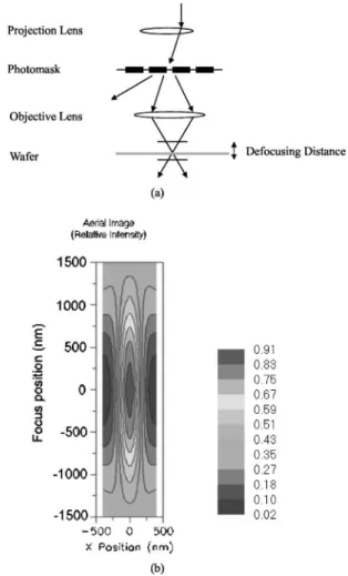
Figure 1.共a兲 Schematic diagram of the exposure system. 共b兲 Relative inten-sity distribution of aerial images near the zero defocus position.
Journal of The Electrochemical Society, 153共9兲 G802-G806 共2006兲
0013-4651/2006/153共9兲/G802/5/$20.00 © The Electrochemical Society
combining conventional optical lithography and RIE process to fab-ricate an optimized pyramid structure by tuning the defocusing dis-tance and exposure dosage of an optical exposure tool. The hexago-nal close-packed arrangement of pyramid structures with low reflection in the 300–800 nm wavelength regimes can be easily achieved by this method.
Experimental
In this paper, we used the rigorous couple-wave analysis and optical thin-film theory to simulate the reflection and transmission properties in a two-dimensional microstructure. In order to fabricate the pyramid structure, we used the commercial optical lithography
Figure 2. Aerial image and resist profile exposed with 共a兲 zero defocus, 共b兲 −0.8m defocus, and 共c兲 +0.8 m defo-cus.
simulator (PROLITH) to simulate the aerial images and cross-sectional profiles of resist under different exposure dosages and de-focusing distances. Experimental parameters can be established by referring to simulation results. The optimal resist profile can be ad-justed by controlling the defocus, exposure dosages, and numerical aperture of a commercial exposure system共I-line stepper, Canon, FPA-3000 i5+兲. In the experimental procedures, silicon wafers were first cleaned with RCA clean processes and then coated with resist by a spin coater and development system共TEL Track, MK-8兲. After the optical lithography processes, the resist patterns were transferred to the substrate by the reactive ion etcher共Anelva, ECR-6001兲 with reactive gases Cl2, SF6, and O2. The reactive-gas flow rates of Cl2,
SF6, and O2are 90, 5, and 5 sccm with 90 W of radio frequency共rf兲
power. Finally, the cross-sectional profile was observed by scanning electron microscopy共JEOL, JSM-6500F兲, and the optical properties were measured by optical spectrometer共Hitachi, U-4100兲. Figure 1a shows the schematic diagram of an exposure system. The defocus-ing distance and exposure dosage can be easily tuned in a conven-tional optical stepper.
Results and Discussion
By using the optical lithography simulator, the aerial images and resist profiles can be simulated under different exposure conditions. The exposure wavelength 365 nm, feature size 400 nm, and numeri-cal aperture 0.6 are fixed in our simulations. Figure 1b shows the relative intensity distribution of aerial images near the zero defocus position. The result indicates that the most relative intensity of aerial image concentrates in the zero defocus region, and the intensity gradually decreases in both the positive defocus and negative defo-cus regions.
Figure 2a shows the aerial image and resist profile of a positive resist with a thickness of 800 nm placed on the zero defocus posi-tion. The z-position in the figure means the distance to the bottom of the resist. The zero defocus means the maximum intensity region is located on the surface of the resist, and the intensity slightly de-creased in other regions. For small intensity gradient in the resist, a vertical resist profile can be obtained by the exposure with a suitable dosage. Similarly, Fig. 2b shows the aerial image and resist profile of a resist exposed with −0.8m defocus. The −0.8 m defocus means the maximum intensity is below the resist surface with 0.8m. In this case, the maximum intensity is located on the bot-tom of the resist and slightly varied in other regions. For small intensity gradient in the resist, a vertical resist profile can also be obtained. Figure 2c shows the aerial image and resist profile of a resist exposed with +0.8m defocus. The +0.8 m defocus means the maximum intensity is above the resist surface with 0.8m. The maximum intensity region is away from the surface of the resist and the relative intensity obviously decreased from the surface to the bottom of the resist. As shown in Fig. 2c, a gradient resist profile can be obtained with positive defocus exposure. The gradient resist pro-files can be used to fabricate pyramid structures on high-reflection substrates.
A suitable exposure dosage is also important for the fabrication of gradient resist profiles. Figure 3a shows the optimized pyramid structures in resists that are simulated in dosage-focus matrix by the optical lithography simulator. According to the simulation results shown in Fig. 3a, we can obtain the optimized pyramid structures in resists by adjusting the exposure dosage and defocusing distance in the range of 165–255 mJ/cm2 and +0.8 to −0.8m, respectively.
These are the referable parameters to fabricate the optimized pyra-mid structures in the resist. Figure 3b shows the reflection spectra of silicon substrates with and without pyramid structures simulated by rigorous couple-wave analysis. Results indicate that the reflectance is dramatically decreased from larger than 40% to less than 2% as the pyramid structures are added on silicon substrates. Therefore, patterning the texturing structures on silicon substrates is desired for eliminating the reflected light.
Figure 4a shows the SEM image of the pyramid structures in the resist in which the period about 0.8m can be obtained by the
suitable exposure parameters of defocusing distance +0.8m and exposure dose 230 mJ/cm2. Figure 4b shows that the SEM image of the pyramid structures were transferred to silicon substrates by RIE with reactive gases Cl2, SF6, and O2. We find the pyramid shape can
remain with the same 0.8m period after the dry etching process. As shown in Fig. 4a and b, the height of the pyramid structure is decreased from 0.68m in the resist to 0.45 m in the silicon sub-strate. This is due to the etching selectivity of about 0.66 between the silicon and resist in our etching process. The height of silicon pyramid structures can also be tuned by tuning the dry etching pa-rameters. Figure 4c shows the cross-section morphology with a large area of close-packed pyramid structures in the silicon substrate can be easily obtained by this method.
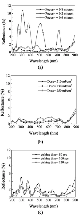
In this study, we fabricated the optimal pyramid structure by tuning the defocusing distance, exposure dosage, and dry etching duration. The texturing structures on silicon substrates fabricated by different process conditions are characterized by measuring the re-flection spectra from deep ultraviolet共DUV兲 to NIR regimes. Figure 5a shows the reflection spectra of the texturing structures fabricated with different defocusing distances but fixed exposure dosage 共230 mJ/cm2兲 and etching time 共100 s兲. Results indicate that the
reflectances are less than 2% for defocusing distance +0.8 and +0.6m. However, the reflectance is about 10% for the +0.2 m defocusing distance, which is insufficient to form the optimal pyra-mid resist structures as simulated in Fig. 3a.
Figure 5b shows the reflection spectra of the texturing structures fabricated with different exposure dosages but fixed defocusing dis-tance共+0.8 m兲 and etching time 共100 s兲. Results indicate that the reflectances are less than 2% for about 10% exposure-dosage toler-ance. Similarly, Fig. 5c shows the reflection spectra of the texturing structures fabricated with different etching times but fixed
defocus-Figure 3.共a兲 Resist profiles dependence of focus-dosage matrix. 共b兲 Simu-lated reflectance spectra of silicon substrates with and without pyramid struc-tures.
G804 Journal of The Electrochemical Society, 153共9兲 G802-G806 共2006兲
ing distance共+0.8 m兲 and exposure dosage 共230 mJ/cm2兲. Results
indicate that the reflectances are less than 5% for different etching times. If we decrease the etching time bias to 100 ± 10 s, a reflec-tance less than 2% can also be obtained. Therefore, we find the defocusing distance in an optical exposure tool is the key factor for the fabrication of optimal pyramid structures. If the resist is exposed at the suitable focusing position, we can get reasonable processing tolerance for the fabrication of pyramid structures by this defocusing method.
Conclusion
Semiconductor-based solar cells have a high refractive index in visible and NIR regimes that cause the high Fresnel’s reflection
between the air/semiconductor interface. Therefore, the key issue for increasing the external quantum efficiency of semiconductor-based solar cells is how to reduce the interface reflection in the solar cell working-wavelength regime. In this paper, we demonstrate a simple method, combining conventional optical lithography and reactive ion etching processes to fabricate an optimized pyramid structure by tuning the defocusing distance and exposure dosage of an optical stepper. Results show the low reflection with broad spectra regimes
Figure 4.共a兲 Resist profile after the development process. 共b兲 Silicon profile after the RIE process.共c兲 Cross-section morphology with a large area of close-packed pyramid structures in the silicon substrate.
Figure 5. Reflectance spectra were obtained共a兲 by varying the defocusing distance of an optical exposure tool,共b兲 by varying the exposure dosage, and 共c兲 by varying the etching time in the RIE process.
are obtained by using the positive defocus exposure in optical li-thography processes. In contrast with previous works, the reflec-tance of texturing structures is affected by optical lithography pro-cesses rather than etching propro-cesses in our works. We also find the defocusing distance in an optical exposure tool is the key factor for the fabrication of optimal pyramid structures. If the resist is exposed at the suitable focusing position, we can get reasonable processing tolerance for the fabrication of pyramid structures by this defocusing method. The exposure parameters can be fine-tuned in an optical stepper. Therefore, the high performance of texturing structures in solar cells with a large area and high reproducibility can be easily obtained. This method is also suitable for the fabrication of antire-flective structures on various kinds of solar cell materials.
Acknowledgment
The authors are very thankful to the National Science Council, Taiwan, for supporting this study under projects NSC-94-2215-E-002-026 and NSC-94-2216-E-002-022.
National Taiwan University assisted in meeting the publication costs of this article.
References
1. I. M. Dharmadasa, Sol. Energy Mater. Sol. Cells, 85, 293共2005兲.
2. M. A. Green, K. Emery, D. L. King, S. Igari, and W. Warta, Prog. Photovoltaics,
11, 39共2003兲.
3. S. Siebentritt, Thin Solid Films, 403-404, 1共2002兲.
4. E. D. Palik, Handbook of Optical Constants of Solids, Academic Press, New York 共1998兲.
5. H. A. Macleod, in Thin-Film Optical Filters, 2nd ed., Adam Hilger, Ltd., Bristol 共1986兲.
6. B. Kumar, T. B. Pandian, E. Sreekiran, and S. Narayanan, in Proceedings of the
31st IEEE Photovoltaic Specialists Conference, p. 1205–1208共2005兲.
7. W. Sonphao, and S. Chaisirikul, in Industrial Electronics 2001, Proceedings of
ISIE 2001, IEEE International Symposium, Vol. 3, pp. 2049–2052共2001兲. 8. J. D. Hylton, A. R. Burger, and W. C. Sinke, J. Electrochem. Soc., 151, G408
共2004兲.
9. R. Bilyalov, L. Stalmans, and J. Poortmans, J. Electrochem. Soc., 150, G216 共2003兲.
10. R. R. Bilyalov, L. Stalmans, L. Schirone, and C. Levy-Clement, IEEE Trans.
Electron Devices, 46, 2035共1999兲.
11. G. Kumalavelu, M. M. Alkaisi, and A. Bittai, in Proceedings of the 29th IEEE
Photovoltaic Specialists Conference, p. 258–261共2002兲.
12. K. Kintaka, J. Nishii, A. Mizutani, H. Kikuta, and H. Nakano, Opt. Lett., 26, 1642 共2001兲.
13. H. Nagayoshi, K. Konno, S. Nishimura, and K. Terashima, Jpn. J. Appl. Phys., Part
1, 44, 7839共2005兲.
14. S. H. Zaidi, D. S. Ruby, and J. M. Gee, IEEE Trans. Electron Devices, 48, 1200 共2001兲.
G806 Journal of The Electrochemical Society, 153共9兲 G802-G806 共2006兲