Formation and composition of titanium oxinitride nanocrystals synthesized via
nitridizing titanium oxide for nonvolatile memory applications
Li-Wei Feng
a,b, Chun-Yen Chang
a,b, Ting-Chang Chang
c,d,⁎
, Chun-Hao Tu
a,b, Pai-Syuan Wang
a,b,
Chao-Cheng Lin
e, Min-Chen Chen
c, Hui-Chun Huang
f, Der-Shin Gan
f, New-Jin Ho
f,
Shih-Ching Chen
c, Shih-Cheng Chen
g,haDepartment of Electronics Engineering, National Chiao Tung University, Hsinchu, 300, Taiwan, ROC bInstitute of Electronics, National Chiao Tung University, Hsinchu, 300, Taiwan, ROC
c
Department of Physics, National Sun Yat-Sen University, Kaohsiung, 804, Taiwan, ROC
d
Center for Nanoscience & Nanotechnology, National Sun Yat-Sen University, Kaohsiung, 804, Taiwan, ROC
e
Green Energy and Environment Research Laboratories, Industrial Technology Research Institute, Hsinchu, 310, Taiwan, ROC
f
Institute of Materials Science and Engineering, National Sun Yat-Sen University, Kaohsiung, 804, Taiwan, ROC
g
Department of Electrical Engineering, National Tsing Hua University, Hsinchu, 310, Taiwan, ROC
hInstitute of Electronic Engineering, National Tsing Hua University, Hsinchu, 310, Taiwan, ROC
a b s t r a c t
a r t i c l e i n f o
Article history:
Received 11 January 2010
Received in revised form 9 April 2011 Accepted 12 May 2011
Available online 19 May 2011 Keywords:
Titanium oxinitride Nanocrystals Nonvolatile memory
Transmission electron microscopy X-ray photoelectron microscopy Capacitance–voltage
Formation and composition analyses of titanium oxinitride nanocrystals (NCs) fabricated via treating a magnetron co-sputtered thinfilm of titanium and silicon dioxide with a rapid thermal annealing in nitrogen ambient were demonstrated for nonvolatile memory applications. Phase separation characteristics with different annealing conditions were examined by transmission electron microscopy and chemical bonding characteristics were confirmed by X-ray photon emission spectra. It was observed that a blanket layer composed mainly of titanium oxide was still present as annealing temperature was increased to 700 °C, associated with the thermodynamically stable phase of titanium oxide. Furthermore, a higher thermal treatment of 900 °C induced formation of a well-separated NC structure and caused simultaneously partial nitridation of the titanium oxide, thereby forming titanium oxinitride NCs. A significant capacitance–voltage hysteresis in threshold voltage shift at 1 V was easily achieved under a small sweeping voltage range of + 2 V/−2 V, and a memory window retention of 2.2 V was obtained after 107s by extrapolation under a 1 s
initial-program/erase condition of + 5 V/−5 V, respectively.
© 2011 Elsevier B.V. All rights reserved.
1. Introduction
In the past few years, portable electronic devices have significantly impacted consumer electronics markets. Because of the low working voltage and non-volatility,flash memory based on a floating-gate structure has been widely employed[1]. However, one problematic area forfloating-gate structures is the limited potential for continued scaling of the device structure. Therefore, in recent years, nanocrystal (NC) nonvolatile memory (NVM) devices with discrete charge trapping centers have been extensively studied and discussed for use with different materials, such as metal NCs, semiconductor NCs
[2–5]and even high-κ dielectric NCs[6–8], due to their ability to
achieve high program/erase speed, low programming voltage, low-power performance and excellent retention and disturb characteris-tics[9–11]. Among these materials, titanium nitride (TiN)[12,13]and titanium oxide (TiO2)[14]NCs have received increasing attention for
NVM applications due to their advantages of high electrical conduc-tivity (TiN)/high dielectric constant (TiO2), larger memory window,
easy fabrication, low cost, good heat stability, and especially excellent compatibility with complementary metal-oxide-semiconductor pro-cesses. Therefore, in this study, titanium oxinitride (TiNxOy) NCs were
investigated for application in NVM because TiNxOymaterials can act
as a conductor (TiN) or an insulator (TiO2) by virtue of a tunable N/O
ratio. There have been many preparation methods for a TiNxOyfilm
reported, such as a reactive sputtering of Ti in an oxygen/nitrogen atmosphere, oxidative annealing of TiN[15], or metalorganic chemical vapor deposition[16,17]. In this study, another simple technique to synthesize TiNxOyin NCs structures was also proposed via treatment
of a magnetron co-sputtered thinfilm of titanium (Ti) and silicon dioxide (SiO2) with a rapid thermal annealing in nitrogen (N2)
ambient.
⁎ Corresponding author at: Department of Physics, National Sun Yat-Sen University, Kaohsiung, 804, Taiwan, ROC.
E-mail address:[email protected](T.-C. Chang). 0040-6090/$– see front matter © 2011 Elsevier B.V. All rights reserved. doi:10.1016/j.tsf.2011.05.042
Contents lists available atScienceDirect
Thin Solid Films
2. Experiment
A ~ 6-nm-thick tunnel oxide measured by transmission electron microscopy (TEM) observation was thermally grown by a dry oxidation process at 875 °C after the standard Radio Corporation of America (RCA) clean process [SPM: H2SO4 (sulfuric acid) + H2O2
(hydrogen peroxide), SC1: NH4OH (ammonium hydroxide) + H2O2+
H2O, SC2: HCl (hydrochloride) + H2O2+ H2O, and HF dip] of a p-type
silicon (100) wafer [18]. Next, a ~ 15-nm-thick Ti-based charge trapping layer was deposited by RF and DC magnetron co-sputtering with SiO2and Ti targets, respectively. The sputtering chamber was
initially evacuated to a base pressure of 2.1 × 10⁻⁴Pa and the working pressure was maintained at 0.61 Pa in argon ambient at room temperature. The RF power of the SiO2 target wasfixed at 100 W
while the DC power of the Ti target wasfixed at 50 W. Then, annealing treatments with different temperature conditions varying up to 900 °C were performed for 1 min in N2(6 N purity) ambient at a pressure of
3 × 10³Pa. A base-pressured evacuation of about 5 × 10⁻⁴Pa was also
performed before the annealing process and the surroundings during rising and lowering of annealing temperature werefilled with N2
ambient. Subsequently, a blocking oxide of 40 nm thickness was deposited by a plasma enhanced chemical vapor deposition system at 300 °C. Finally, a 500-nm-thick aluminum (Al) gate electrode was deposited by thermal evaporation and patterned by a shadow mask with a pad radius of 0.4 mm to form a capacitor structure for electrical measurement. The schematic diagram of device structure is shown in the inset ofFig. 1a. TEM and X-ray photon emission spectra (XPS) were adopted for the microstructure analysis and chemical material analysis of the NCs, respectively. Note that the XPS analyses were carried out using a Microlab 350 with a monochromatized Al Kα X-rays source (1486.6 eV; 300 W) with XPS data adopted from the annealed samples before capping the blocking oxide. Cross-sectioned TEM samples were prepared using the focused ion beam system (FIB, SEIKO SMI3050SE; ion beam operating at 30 kV and 200–7000 pA) lift-out method and analyzed by a Philips Tecnai-20 System operating at an accelerating voltage of 200 kV. The sample thickness was about 80 nm. In addition, electrical characteristic measurements, including the capacitance–voltage (C–V) hystereses and retention characteristics, were performed by a HP4284 Precision LCR Meter with high frequency of 1 MHz.
3. Results and discussion
To observe the phase separation after the different annealing conditions, TEM image analyses were performed.Fig. 1shows the cross-sectional TEM images of the Ti/SiO2co-sputtered samples with
annealing temperatures of (a) 500 °C, (b) 700 °C, and (c) 900 °C in N2
ambient for 1 min. InFig. 1a, a continuous trapping layer structure was still observed after an annealing treatment of 500 °C. However, when the annealing temperature was increased to 700 °C, the trapping layer was observed to segregate partially and incompletely, as shown in
Fig. 1b. Furthermore, after the 900 °C annealing treatment, observation of clear NC dot structures was visually confirmed, shown inFig. 1c, where an NC density of ~6.2 × 1010cm−2could be roughly estimated.
The NCs were most probably surrounded by SiO2 as the brighter
contrast with the NCs confirms, which corresponds to the XPS results discussed later. In addition, on the basis of the strong variations in contrast of the Ti-contained region between TEM images inFig. 1, it would be reasonable to suspect a substantial migration of Ti out of the TiO2layer. Further, an expansion of the NC size to ~ 20 nm in diameter
was also observed, which could be due to the severe thermal diffusion of the trapping layer after undergoing such a high annealing temperature treatment. The migration of Ti into the substrate is less than out-diffusion. This suggests that the migration of larger Ti atoms into the Si substrate would severely damage the tunneling oxide quality and then severely degrade the retention characteristic, which
is unobserved in our results. Moreover, we also analyze the NCs by Fourier transformation with Gatan tool from the TEM sample, which detected the TiO, Z = [011] as shown in the inset ofFig. 1c.
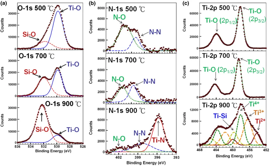
Fig. 2shows comparisons of XPS for O-1s, N-1s, and Ti-2p for the Ti/SiO2co-sputtered samples with annealing temperatures of 500 °C,
700 °C, and 900 °C in N2 ambient. Energy calibration, necessary
because of charging effects, was performed using the adventitious carbon C-1s peak at 284.7 eV. In O-1s spectrum, the main peak signal for Ti–O binding at 530 eV was observed in the 500 °C-annealed sample [19]. The Ti atom is easily oxidized since TiO2 is a
thermodynamically stable phase, and hence, the trace O2existing in
the co-sputtering process or the absorbed O2on the wafer surface
during wafer transportation (air exposure) is enough to cause the
Fig. 1. Cross-sectional TEM images of the Ti/SiO2co-sputtered samples with annealing
temperatures of (a) 500 °C, (b) 700 °C, and (c) 900 °C in N2ambient for 1 min. A
schematic diagram of device structure is shown in the inset of a. The inset of c shows the NCs by Fourier transformation with Gatan tool.
Fig. 2. Comparisons of XPS for O-1s, N-1s, and Ti-2p on the Ti/SiO2co-sputtered samples with annealing temperatures of 500 °C, 700 °C, and 900 °C in N2ambient. 7979 Feng et al. / Thin Solid Films 519 (2011) 7977 – 7981
formation of Ti–O bonding during the rapid annealing process[20,21]. As the annealing temperature was increased to 700 °C, the peak signal was observed at 532.6 eV, referencing Si–O binding, and was obviously enhanced while the intensity of the Ti–O peak decreased relatively[22]. Furthermore, after the 900 °C-annealing treatment, the Si–O peak began to dominate rather than the Ti–O bond. The increase of Si–O bonds and the decrease of Ti–O bonds with an increase in annealing temperature are associated with the formation of silicon dioxide around the NCs, inferred from the TEM results, as well as the partial replacement of Ti–O bonds by Ti–N bonds. In the N-1s spectrum, observations of peak signals around 400 eV and 402 eV in
the samples with the 500 °C and 700 °C annealing temperatures, respectively, were representative of molecularly chemisorbedγ-N2,
caused from a small amount of N2molecules incorporated into the
TiO2 lattice [23]. As the annealing temperature was increased to
900 °C, a peak signal at 397 eV is clearly observed, contributed from the formation of atomic β-N [23]. Moreover, the occurrence of a positive shift of + 1 V in binding energy when compared to normal Ti–N bond (396 eV) confirms the formation of titanium oxinitride bindings due to the existence of higher electronegative oxygen atoms. According to reference [22], TiN dissolution and TiOxformation are
thermodynamically favored; however, observations of these abnormal binding formations in our experiment are presumably driven by the excess of N2 in this co-sputtered charge trapping layer. It is also
mentioned that silicon nitride might also be composed while such a high temperature annealing condition is treated on the sample, but the influence of SiN could be ignored here according to the unobvious observation of Si–N peak in the N-1s spectrum, compared to the Ti–N peak. In the Ti-2p spectrum, two detectable principal peaks close to 464 and 458 eV in the samples with the 500 °C and 700 °C annealing temperatures, respectively, are representative of Ti4+-2p
1/2
and Ti4+-2p
3/2, contributed from titanium dioxide bonds[24]. Detection
of these bonds also corresponds to the results of the O-1s spectrum due to the existence of the thermodynamically stable phase of TiO2.
However, a significant broadening of the Ti-2p lines on the lower binding energy side occurs in the sample with the 900 °C annealing temperature due to the formations of Ti3+and Ti2+bindings[25]as well
as the Ti–Si binding at 459 eV[26]. The observation of Ti3+and Ti2+
peaks also confirms the occurrence of nitridizing TiO2.
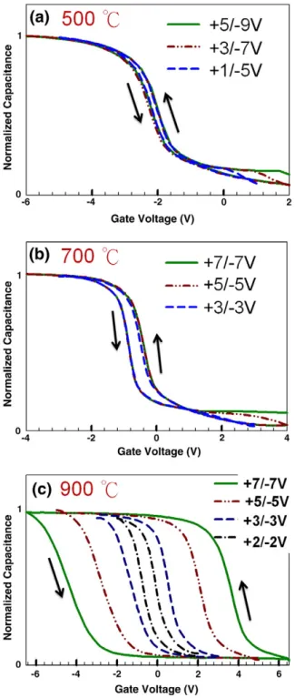
Fig. 3shows C–V characteristics of different gate voltage sweeping regions on the Ti/SiO2 co-sputtered samples with annealing
treat-ments of (a) 500 °C, (b) 700 °C, and (c) 900 °C. As shown inFig. 3a, no threshold voltage shifts occurs for the 500 °C sample. Moreover, the C–V curve shifts along the negative voltage axis, which is associated with the existence of positivefixed charge in the TiO2layer. This
suggests, therefore, that a blanket TiO2 layer exhibits no
program-mable/erasable charge trapping centers for NVM applications. As the annealing temperature was increased to 700 °C (Fig. 3b), small threshold voltage shifts occur due to partial and incomplete segrega-tion in the trapping layer. Furthermore, after the 900 °C-annealing condition, outstanding threshold voltage shifts of ~2 V, ~5 V, and ~ 8 V are exhibited, increasing with an increase in the gate voltage sweeping regions of 3/−3 V, 5/−5 V, and 7/−7 V, respectively. A threshold voltage shift of 1 V is easily achieved under a small sweeping voltage range of 2 V/−2 V. Explicit observation of the threshold voltage shift is mainly due to the formation of well-separated NC structures instead of
Fig. 3. C–V characteristics of different gate voltage sweeping regions on the Ti/SiO2
co-sputtered samples with annealing treatments of (a) 500 °C, (b) 700 °C, and (c) 900 °C. The arrows indicate voltage sweeping directions.
Fig. 4. Charge loss characteristic of the TiNxOyNC capacitor with the annealing
treatment of 900 °C. 7980 L.-W. Feng et al. / Thin Solid Films 519 (2011) 7977–7981
a continuous trapping layer structure, which would result in a stored carrier charge possessing lateral leak. This indicates that the TiNxOyNCs provide excellent characteristics for acting as charge
storage centers for NVM applications, especially their potential for low power operation device applications. In addition, observation of the counterclockwise hysteresis loops of the C–V curves indicates the phenomenon of substrate injection of carriers through the tunneling oxide, which is preferable to gate injection through the blocking oxide.
Fig. 4 shows the charge loss characteristic of the TiNxOy NC
capacitor with the annealing treatment of 900 °C. After an initial-program/erase bias condition of 5 V/−5 V for 1 s, the threshold voltage shift still remains about 2.2 V after 107s by extrapolation,
indicating excellent charge storage characteristic of TiNxOyNCs for
NVM applications.
4. Conclusion
This study investigates material analyses and the formation of TiNxOyNCs fabricated by co-sputtering titanium and silicon dioxide
targets with different annealing conditions in N2ambient. A 900
°C-annealing treatment induced a well-separated NC structure and nitridation of the titanium oxide to form the TiNxOy NCs, which
provide high electrical performance for NVM applications. A signif-icant C–V hysteresis of threshold voltage shift in 1 V is observed under the low operating voltage of + 2 V/−2 V voltage sweeping. The retention characteristics were also tested to be robust.
Acknowledgments
This work was performed at the National Nano Device Laboratory and was supported by the National Science Council of the Republic of China under contract no. NSC 96-2221-E-009-202-MY3, no. NSC 97-2112-M-110-009, no. NSC 009-001, no. NSC 98-2221-E-009-002, and no. NSC 98-3114-M-110-001.
References
[1] D. Kahng, S.M. Sze, Bell Syst. Tech. J. 46 (1967) 1288.
[2] F.M. Yang, T.C. Chang, P.T. Liu, P.H. Yeh, Y.C. Yu, J.Y. Lin, S.M. Sze, J.C. Lou, Appl. Phys. Lett. 90 (2007) 132,102.
[3] C.H. Chen, T.C. Chang, I.H. Liao, P.B. Xi, C.T. Tsai, P.Y. Yang, Joe Hsieh, Jason Chen, U.S. Chen, J.R. Chen, Appl. Phys. Lett. 91 (2007) 232,104.
[4] W.R. Chen, T.C. Chang, Y.T. Hsieh, S.M. Sze, C.Y. Chang, Appl. Phys. Lett. 91 (2007) 102,106.
[5] F.M. Yang, T.C. Chang, P.T. Liu, U.S. Chen, P.H. Yeh, Y.C. Yu, J.Y. Lin, S.M. Sze, J.C Lou, Appl. Phys. Lett. 90 (2007) 222,104.
[6] S.M. Yang, C.H. Chien, J.J. Huang, T.F. Lei, Appl. Phys. Lett. 91 (2007) 262,104. [7] Y.H. Lin, C.H. Chien, C.T. Lin, C.Y. Chang, T.F. Lei, IEEE Trans. Electron Devices 53
(2006) 782.
[8] H.C. You, F.H. Ko, T.F. Lei, J. Electrochem. Soc. 153 (2006) F94.
[9] R. Muralidhar, R.F. Steimle, M. Sadd, R. Rao, C.T. Swift, E.J. Prinz, J. Yater, L. Grieve, K. Harber, B. Hradsky, S. Straub, B. Acred, W. Paulson, W. Chen, L. Parker, S.G.H. Anderson, M. Rossow, T. Merchant, M. Paransky, T. Huynh, D. Hadad, K.-M. Chang, B.E. White Jr., IEDM Tech. Dig. (2003) 26.2.1.
[10] C. Lee, A. Gorur-Seetharam, E.C. Kan, IEDM Tech. Dig. (2003) 22.6.1.
[11] T. Baron, B. Pelissier, L. Perniola, F. Mazen, J.M. Hartmann, G. Rolland, Appl. Phys. Lett. 83 (2003) 1444.
[12] S. Choi, S.S. Kim, M. Chang, H. Hwang, S. Jeon, C. Kim, Appl. Phys. Lett. 86 (2005) 123,110.
[13] S. Mailap, P.J. Tzeng, H.Y. Lee, C.C. Wang, T.C. Tien, L.S. Lee, M.J. Tsai, Appl. Phys. Lett. 91 (2007) 043114.
[14] C.H. Lin, C.C. Wang, P.J. Tzeng, S. Maikap, H.Y. Lee, L.S. Lee, M.J. Tsai, Jpn. J. Appl. Phys. 46 (4B) (2007) 2523.
[15] T. Morikawa, R. Asahi, T. Ohwaki, K. Aoki, Y. Taga, Jpn. J. Appl. Phys. 40 (2001) L 561.
[16] S.W. Yang, L. Gao, J. Am. Ceram. Soc. 87 (2004) 1803.
[17] J. Guillota, F. Fabreguetteb, L. Imhoffa, O. Heintza, M.C. Marco de Lucasa, M. Sacilottib, B. Domenichinia, S. Bourgeois, Appl. Surf. Sci. 177 (2001) 268. [18] J.D. Plummer, M.D. Deal, P.B. Griffin, Silicon VLSI Technology Fundamentals,
Practice and Modeling, Prentice-Hall, Upper Saddle River, NJ, 2000.
[19] H. Noda, K. Oikawa, T. Ogata, K. Matsuki, H. Kamada, Chem. Soc. Jpn. 8 (1986) 1084.
[20] C.H. Lin, C.C. Wang, P.J. Tzeng, C.S. Liang, W.M. Lo, H.Y. Li, L.S. Lee, S.C. Lo, Y.W. Chou, M.J. Tsai, Jpn. J. Appl. Phys., Part 1 1 (45) (2006) 3036.
[21] J.M. Wang, W.G. Liu, T. Mei, Ceram. Int. 30 (2004) 1921. [22] T.L. Barr, J. Phys. Chem. 10 (1990) 760.
[23] N.C. Saha, H.G. Tompkins, J. Appl. Phys. 72 (1992) 3072.
[24] S. Petigny, H. Mostefa-Sba, B. Domenichini, E. Lesniewska, A. Steinbrunn, S. Bourgeois, Surf. Sci. 410 (1998) 250.
[25] J. Guillota, F. Fabreguetteb, L. Imhoffa, O. Heintza, M.C. Marco de Lucasa, M. Sacilottib, B. Domenichinia, S. Bourgeois, Appl. Surf. Sci. 177 (2001) 268. [26] W.Y. Yang, H. Iwakuro, H. Yagi, T. Kuroda, S. Nakamura, Jpn. J. Appl. Phys. 23