ELSEVIER Physica B 205 (1995) 183-192
Effect of phonon scattering on free-carrier absorption in n-type
indium antimonide films
C h h i - C h o n g W u a' *, C h a u - J y L i n b
alnstitute of Electronics, National Chiao Tung University, Hsinchu, Taiwan bDepartment of ,4pplied Mathematics, National Chiao Tung University, Hsinchu, Taiwan
Received 15 March 1994; revised 27 July 1994
Abstract
The free-carrier absorption in n-type InSb films has been investigated for carriers confined in quasi-two-dimensional (2D) semiconductors with the nonparabolic energy band of electrons. We discuss the effect of phonon scattering on the free-carrier absorption coefficient (~) for both deformation-potential coupling and piezoelectric coupling. ~ is found to depend on the photon polarization relative to the direction normal to the quasi-2D structure, the photon frequency, the film thickness, and the temperature. ~ could be complex due to the interaction between photons, phonons, and electrons. (i) When the acoustic phonon scattering is dominant, ~ increases with decreasing the film thickness for phonons polarized parallel or perpendicular to the layer plane. It is also shown that ~t increases with decreasing photon frequency and increasing temperature for photons polarized parallel to the layer plane, while for photons polarized perpendicular to the layer plane the ct temperature-dependence is more complicated. (ii) If the piezoelectric scattering is dominant, ~ is also decreasing with increasing the film thickness for photons polarized parallel or perpendicular to the layer plane. But ct decreases with increasing temperature for photons polarized perpendicular to the layer plane. Moreover, numerical results for the parallel polarization are much smaller than those for the perpendicular polarization.
1. Introduction
There has been a growing interest in the elec- tronic and optical properties of semiconducting layered heterojunctions [1-6], thin films I-7, 8], and inversion layers [9-11]. Due to the confinement of carriers in these quasi-two-dimensional structures, size quantization begins to play an important role in determining their electronic and optical proper- ties. The optical absorption can take place via di- rect interband transitions, and intersubband * Corresponding author.
transitions, and indirect intraband transitions in which the carriers absorb or emit a photon while simultaneously scattering off phonons or other im- perfections. Such free-carrier absorption accounts for absorption of photons with frequency f2 lower than the band gap Eg of semiconductors, i.e., hf2 < E~. In a magnetic field, where the carrier motion is confined to a plane perpendicular to the magnetic field, the free-carrier absorption coeffic- ient (~) depends upon the photon polarization rela- tive to the magnetic field [12]. For carriers con- fined in a quasi-2D structure, it was found that depends upon the photon polarization relative to
0921-4526/95/$09.50 © 1995 Elsevier Science B.V. All rights reserved SSDI 0 9 2 1 - 4 5 2 6 ( 9 4 ) 0 0 6 1 8 - 0
184 C.-C Wu, C-J. Lin / Physica B 205 (1995) 183-192
the direction normal to the quasi-2D structure [13]. In III-V semiconductors, the acoustic- phonon-carrier interaction is dominated by the deformation-potential and piezoelectric couplings [14].
In this paper, we investigate the quantum theory of the free-carrier absorption in III-V semiconduc- tors with the nonparabolic energy band of electrons with a quasi-2D structure. It has been shown that the nonparabolicity of the energy band in semicon- ductors can be used to explain the longitudinal magnetoacoustic phenomenon [ 15] and the acous- tic-surface-wave amplification [14]. In this calcu- lation, we consider a nondegenerate electron gas with a Maxwell-Boltzmann distribution for non- degenerate semiconductors. Thus, we make follow- ing assumptions:
(1) For a nondegenerate semiconductor, the dis- tribution function of electrons can be represented by the Maxwell-Boltzmann distribution. The effect of Fermi energy can be neglected for the non- degenerate electron gas in a nondegenerate semiconductor [13].
(2) The interaction between electrons and acous- tic phonons originates from the deformation-po- tential and piezoelectric couplings in III-V semiconductors.
(3) The energy band of electrons in semiconduc- tors is assumed to be of nonparabolicity.
In Section 2, we recall the electronic states of a quasi-2D structure for the nonparabolic band structure. In Section 3, we present the quantum theory of the free-carrier absorption with confined carriers in nondegenerate semiconductors for the deformation-potential and piezoelectric couplings. We discuss two special cases: the photon is polariz- ed parallelly or perpendicularly to the layer plane. In Section 4, some numerical results of the free- carrier absorption coefficient are presented for n- type InSb. Finally, a brief discussion about our numerical analysis is given.
2. Electronic states in a thin semiconductor layer
The motion of conduction electrons parallel to the thin films may be described by plane waves, and those perpendicular to the surface will be described
by the type of standing waves depending on the structure of potential. For a square well potential along the z axis with infinitely high barriers at z = 0 and z = d, the electron field operator ~*(r) is given [16] by
~+(r) ~, ~ , b ~ n e x p ( - i k ~ [ n n z \ = .=1 k "x)sin ~---d-) '
(I)
where r = (x, z) = (x, y, z), V = dS is the film vol- ume, S being the surface area, and d the film thick- ness, k = (kx, k r) is the electron wave vector in the x - y plane, and bk*, is the electron creation operator. The electron energy Ekn is given [14, 17-19] by the relation
Ek,~ h 2 k 2 n 2 h 2 n 2 ek, = Ek, l + --E-~g ) = ~gm. -~- 2m.d---~,
n = 1, 2, 3, . . . , (2)
where m* is the effective mass and ek, is the effective eigenvalue due to the effective Hamiltonian [19]. The electron energy for the nonparabolic band Ek, in Eq. (2) can be written as
+ \E,] \2m* + 2-2-m--Vd~]] J
n = 1, 2, 3, ... (3)
Since (h2k2ax)/2m* + (nhn)2/2m*d 2 _~ kBT < Eg for T ~< 300 K, Eq. (3) can be expanded as
Et, n ~- - ½E~ + ½E~a, + h2k2/2m*a. (4) with a. = [1 + (2n2h2n2)/(m*d2Eg)] 1/2. (5) In the case of low photon energies, the electron energies received from the photons are also small. Thus only low quantum numbers will contribute to the system. Thus we may expand a. from Eq. (5) for the second term of Eq. (4) and obtain the expression
n 2 h 2 n 2 h 2 k 2
E~n ~- 2m.d----~ + 2m* (6)
with m* = m*a,. This expression for Ek~ is almost the same type as shown in Ref. [19]. In our present work, we consider any values of photon energies, and the energy received by electrons is not so small. Hence we use the nonparabolic band of electrons as
C.-C. Wu, C.-J. Lin/Physica B 205 (1995) 183 192 185 shown in Eq. (4). It is seen that Eq. (6) can be
reduced to the parabolic band of electrons in semiconductors as the parameter a, is taken to a limit one. Since the quantum number n cannot be zero, thus the parabolic band of electrons is only a limit model of the nonparabolic band of electrons in III-V semiconductors.
where ~ is the photon polarization vector and p is the electron momentum. Its matrix elements for electrons in the same band are given as follows:
(i) When the photon is polarized parallelly to the layer plane,
<k'n'lH~adlkn>
3. Quantum theory of free-carrier absorption in
quasi-2D nondegenerate semiconductors
The absorption coefficient ~ for the absorption of photons can be expressed [-13] as
El/2
= - - ~ W, f~, (7)
n 0 c "~-.
where ~ is the dielectric constant of material, no is the number of photons in the radiation field,f~ is the distribution function of carriers and Wi is the transition probability. It is given with the Born approximation
2 ~
W g - ~ - f ~ [ l < f l M +
li>126(Ef - E~ - hK2 - hc%)
+ I<flM-li>12,~(Ef - E~- ht2 +
h~%)-I,(8)
where Ei andE:
are the initial and final electron energies, hQ is the photon energy, h~% is the phonon energy. For interaction between electrons, photons, and phonons, the transition matrix ele- ments<fire+ li)
are given by<flM+_
Ii)V
l Ej - Ei T- hogq
< fl Vslj)__~jtHradli>
~
+ Ej -- E~ - hf2 J ' (9) w h e r e H r a d is the electron-photon interaction and V, is the scattering potential due to the elec- t r o n - p h o n o n interaction.
The electron-photon interaction is given by
e_(_( 2nhno ~ 1/2
Hrad-
m*\
eOV /
n'P'
(10)
e (2~hno~ 1/2
-
~ \ ~ / t
e'(hk)6"""6kx'kx6k~'kY"
(11)(ii) When the photon is polarized perpendicular- ly to the layer plane,
ieh(2nhno~e/2(d )
(k'n'lHradlkn)
= m * \ef2V ]
J'l -- cos [•(n' + n)] x n' + n 1 -- cos[n(n' -- n ) ] ] + n ' - - nXfk, kxfk, ky.
(12)The distribution function for a quasi-2D non- degenerate electron gas in nondegenerate semicon- ductors can be expressed as
f~" = \2n2m*kaT]
[_,=1 2--~sTJ]I Egan h2k 2
, (13)
xexp 2kBT 2m kBTa.J where ne is the concentration of electrons.
For III-V semiconductors, there are two domi- nant electron-phonon scattering mechanisms:
3.1. Deformation-potential coupling
When the deformation-potential coupling is dominant, the electron-phonon potential [18, 20] reads
knT
x~ 1/2Vs = \2pv2V ]
Edexp(iq.r),
(14)where p is the density of material, vs is the sound velocity, q is the phonon wave vector, and Ed is the deformation potential. For wave functions given in
186 C.-C. Wu, C.oJ. Lin /Physica B 205 (1995) 183-192
Eq. (1), one can have
I ( kBT "~ 1/2
(k' n'lVslkn) = ~ \2pv2V j
EdC~kx,kx+qx6k~.k,+q,X [(}q:, (n/d) in' - n) + (~q:, - ~nla)~n" - .)
- - (~q:. (n/d)(n' + n ) - - (~qz. - ( n / d ) ( , '
+,)1"
(15) From Eqs. (7)-(9), (11)-(13) and (15), the free- carrier absorption coefficient for a quasi-2D elec- tron gas can be obtained as shown in Appendix. From Eqs. (A.1) and (A.7), it can be seen that the free-carrier absorption coefficient could be complex coming from the logarithmic functions due to the interaction between electrons, photons and phonons.
3.2. Piezoelectric coupling
When the piezoelectric coupling is dominant, the electron-phonon potential is given [18] by
( kBT ~1/2 lelflPexp(iq.r)
(16)Vs = \2pv2 V /
eq
where tip is the appropriate piezoelectric constant. For wave functions given in Eq. (1), one can have
1 ( kaT y/2 lelfle
(~k,x,kx+q x(k'n'lVslkn) = 2t,2pv~VJ
eq
X 6k~,, ky+qy [(~q=, (n/d)(n'-n) "~ (~qz, -(n/d)tn'-n) - ($~., (ntd~(." +.~ - - 6q=, - (n/d){.' +.)1. (17)
From Eqs. (7)-(9), (11)-(13) and (17), the free- carrier absorption coefficient for a quasi-2D elec- tron gas can be obtained as in Appendix. From Eqs. (A.12) and (A.15), it can also be seen that the free-carrier absorption coefficient could be complex coming from the logarithmic functions in there due to the interaction between electrons, photons, and phonons.
4. N u m e r i c a l analysis and discussion
In this section, a numerical example is developed for an n-type nondegenerate InSb thin film. The
relevant values of physical parameters are taken to be [15, 211 ne = 1.75 × 1014cm -3, m* = 0.013too (too is the free electron mass), p = 5.8 gm/cm 3, e = 1 8 , E g = 0 . 2 e V , E d = 4 . 5 e V , f i e = 1.8×10⁴ esu/cm 2 and vs = 4 x 105 cm/s.
4.1. Deformation-potential coupling
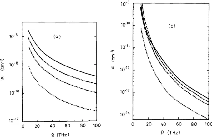
In Fig. 1 (a), the free-carrier absorption coefficient in n-type InSb films is plotted as a function of the photon frequency with d = 10 Ixm for photons po- larized parallelly to the layer plane. Since the real and imaginary parts of ~ have the same order of numerical values,
I~1
appears monotonically de- creasing with increasing the photon frequency [22]. It can also be seen thatI c<l
increases with temper- ature. We plot the free-carrier absorption coeffic- ient in n-type InSb films as a function of the photon frequency with d = 10 txm for photons polarized perpendicularly to the layer plane as shown in Fig. l(b). Since the imaginary part of~ is quite small compared with the real part of ~, hence ~ -~ I ~1 for this case [221. It can be seen that ~ decreases with increasing the photon frequency. However, the changing of c~ with temperature appears irregularly in lower frequencies with O < 25THz at higher temperatures such as T = 77 and 300 K. In Fig. 2(a), we plot the free-carrier absorption coefficient as a function of the film thickness with the photon frequency f2 = 28 THz (or 10.6 lxm wavelength of CO2 laser) for photons polarized parallelly to the layer plane. It is shown thatI~1
decreases with increasing the film thickness and increases with temperature. In Fig. 2(b), we plot the free-carrier absorption coefficient as a function of the film thickness with 12 = 28 THz. Since the imaginary part of ~ appears some significant values only with d < 0.4 Ixm except at T = 4.2 K in which the imagi- nary part of ~ vanishes [221, thus it can also be approximated as ~ -I~1
except T = 4.2K. It is shown that ~ decreases with increasing the film thickness. However, the changing of ~ with temper- ature does not appear in a regular trend. Some small oscillations of the free-carrier absorption co- efficient with the changing of the film thickness demonstrate the confinement of electrons in these quasi-two-dimensional structures. This phenom- enon is coming from the interaction betweenC.-C. Wu, C.-J. Lin / Physica B 205 (1995) 183 192 I0 -9 I~ II 187 10 -6 i: Io -B 10-10 i0-12
-....
--.. --..._
% %%. ,.. IIII1"~1"1~1 "~1 "'1~'111 I! t1111 I IIII'E
U vi0-~o
10-~110-12
i0-1310-+4
(b)
NNN
-'.
~. -,
-...
%°% "~,+~ "% %-°++ "'% %, , I I , I I , 0 20 40 60 B0 100 0 20 40 60 80 100(THz)
(THz)
Fig. 1. Free-carrier absorption coefficient in n-InSb films due to acoustic phonon coupling as a function of photon frequency with d = 10 lam for photons polarized (a) parallel and (b) perpendicular to the layer plane for various temperatures: T = 300 K (----), T = 7 7 K ( ), T = 19.7K( . . . . ), and T = 4.2K ( ... ).
photons, phonons, and electrons in nondegenerate semiconductors.
4.2. Piezoelectric coupling
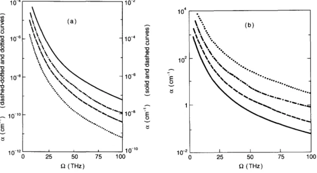
We plot the free-carrier absorption coefficient in n-type InSb films as a function of the photon fre- quency with d = 10 ~tm for photons polarized par- allel to the layer plane as shown in Fig. 3(a). Since the values of the imaginary part of ~ are quite small compared to those of the real part of ~ [22], thus ~1~1. It can be seen that ~ decreases monotoni- cally with increasing the p h o t o n frequency and increases with temperature. While for photons po- larized perpendicularly to the layer plane as shown in Fig. 3(b), it is shown that ~ decreases monotoni- cally with increasing the photon frequency, but decreases with increasing temperature. This is
different from that in Fig. 3(a) for photons polariz- ed parallel to the layer plane. F o r this case, the imaginary part of ~ appears quite small compared with the real part of ct in the order of 10- 6 [-22]. In Fig. 4(a), the flee-carrier absorption coefficient is plotted as a function of the film thickness with t2 = 2 8 T H z (or 10.6 Mm wavelength of CO2 laser) for photons polarized parallel to the layer plane. It can be seen that ~ decreases monotonically with increasing the film thickness and also increases with temperature. In Fig. 4(b), we plot the flee- carrier absorption coefficient as a function of the film thickness for photons polarized perpendicular- ly to the layer plane with f2 = 28 T H z (or 10.6 ~tm wavelength of CO2 laser). It can be seen that in low temperatures ~ decreases monotonically with in- creasing the film thickness. But ct decreases with increasing temperature after the film thickness
188 C.-C Wu, C.-J. Lin / Physica B 205 (1995) 183-192 E 10 -1 1 0 - 3 10-5 10 - 7 1 0 - 9 10 -11
-",..?'.,',X
".... " . \ \ \
• -.. • .. "\ \"...
"-:..
".. " \ k - \ -.. "; i . . . I . . . .,J 10 -1 1 I0 1 0 - 3 10-5 10-7 "7 E - 10- 9 1 0 -11 10 -I 3 ( b ) • ". ",,k%
... 10 -1 1 10 d Clam) d (lam)Fig. 2. Free-carrier absorption coefficient in n-InSb films due to acoustic phonon coupling as a function of the film thickness with Q = 28 THz for photons polarized (a) parallel and (b) perpendicular to the layer plane for various temperatures: T = 300 K ( ), T = 7 7 K ( -), T = 19.7K ( .. . . . ), and T = 4.2K ( ... ).
d = 3 x I0-1 lam. This is different from that Fig. 4(a). However, at higher temperatures such as T = 77 and 300 K, ~ oscillates with the film thick- ness in a region of small thickness of films, d < 3 x 10⁻¹ ~tm, and then decreases monotoni- cally with increasing the film thickness. This is coming from the fact that there exists a cusp min- imum point in the real part of ~ and there are some oscillations in the imaginary part of ~ in the region d < 3 x 10 -1 lam [22]. Moreover, the real and imaginary parts of ~ in this region appear the same order of numerical values. After passing this region, the imaginary part of ~ drops abruptly and discontinuously to a quite small value compared with the real part of ~ as T = 77 and 300 K for the effect of phonons becoming more considerably.
F r o m our numerical results presented here, it is shown that the free-carrier absorption coefficient in n-type InSb films depends upon the photon polar-
ization, the p h o t o n frequency, the film thickness, and the temperature. When the acoustic p h o n o n scattering is dominant, the free-carrier absorption coefficient appears irregular dependence on tem- perature for photons polarized perpendicularly to the layer plane. However, when the piezoelectric scattering is dominant, the free-carrier absorption coefficient increases with decreasing temperature for photons polarized perpendicularly to the layer plane. Thus the dependence of temperature on the free-carrier absorption coefficient for the piezoelectric scattering is quite different from that for the deformation-potential scattering in this kind of polarization. We have also shown that the effect of the nonparabolicity of electrons in semiconductors will be relevant at high electron energy and thus a high photon energies. At low frequencies the parabolic band of electrons is a rea- sonable approximation. The deviation for the approximation at low frequencies will be from
C.-C. Wu, C.-J. Lin / Physica B 205 (1995) 1 8 3 - 1 9 2 189 o t-- t~ 0 -? i1) e.,- ff) E o v 10 - 4 i 0 - o 10 -a 10 -10 10 2 10 . 4 . ~ ( a ) \ \ \ • -. \ % . ".... \ \ . °%.° ~ _ ~ , °°%"° % ~ , , 7'5 25 50 f~ (THz) 10-o 10 -a ¢.) "o "o "o "5 0~ v i E o 104 102 E
~"..
(b)~\ "..
\ - . - . X \ "....-...
\ , , , - , . , .
.. ...
_ 10 - 1 2 10 -1° I 0 -2 I I I 0 1 0 0 0 2 5 5 0 7 5 1 0 0 f~ ( T H z )Fig. 3. Free-carrier absorption coefficient in n-InSb films due to piezoelectric coupling as a function of photon frequency with d = 10 ~tm for p h o t o n s polarized (a) parallel and (b) perpendicular to the layer plane for various temperatures: T = 3 0 0 K ( - - ) , T = 7 7 K ( - - - ) , T = 19.7K ( . . . ), a n d T = 4 . 2 K ( ... ).
Eqs. (4)-(6) as
l ~ 2 h 4 k 2 n 2
A E k , - 2m,E d2Eg .
This is very small if we take a limit n -- 1.
(18)
Acknowledgement
This study was supported by N a t i o n a l Science Council, Republic of China, under contract num- ber: NSC-81-0404-E009-539.
Appendix
Deformation-potential coupling
(i) When the photon is polarized parallel to the layer plane, 1= l nI ~ L g(U,i)- + 47nin I + nz7 -
LT ~ \ ~ )
- ~7 2(n I + 2n/)21n U 2 = - 1 +~ 1 1}"}-~2=-11 ~ , ).(U/~f)_ 1 + 5 7ninf , (A.1)
where
2n4 eEn~kB T E 2
C~D = f2aellE p v 2 m , c d a h 2 , (A.2)
(nv,y
190 C.-C. Wu, C.-J. Lin / Physica B 205 (1995) 183 192
'E
U v 10 3 10 10 -1 10-3 10-510-7
"..\
- \
(a)
" X
_-,. \
- \
',,
~ "% \% 10 5 10 4 ---_ 10 3 010 2
10
A
IIrl
( b )
°eooe Q°oeo e Qe % °. ~e • o",.,,
"\%
..
• %%1" \
%. I ~ I I 10 10 2 I0 -I I 10 10 2d (I..tm)
d (larn)
Fig. 4. Free-carrier absorption coefficient in n-InSb films due to piezoelectric coupling as a function of the film thickness with D = 28 THz for photons polarized (a) parallel and (b) perpendicular to the layer plane for various temperatures: T = 300 K ( ), T = 7 7 K ( - - - ) , T = 19.7K ( . . . ), and T = 4.2K ( ... ).
hEk 2
kilT = zEg -
2m* '
(A.4)
1
U ~ = ~,(n: +_
n,) 2 - ~
(A.5)
and
N :can be determined from
ni < N f <~ ni + df2/ltvs.
(A.6)
(ii) When the photon is polarized perpendicular-
ly to the layer plane,
(
at
~
~
(n,)2 = ~D t a, exp -- ~ : J ni=l n.f=l n'=l[1-- cos ,(n: + n')
1--cosTt(n:--n'!] 2
X ani n f -t- n" '~ n f - - ~'(_a4{ £', :.V,',_+
+*.:4
x exp
2~J
In
~ = _ 1\v,; +-£~,~)
+ 1 + 1 + ~,' ~ ' I V ; I - - 2]exp[2V,'~- E;f] # = - 1 ) . = - 1x E,[ -
).v;# +
E~:]},
where
(A.7)
f ~tv,h \ ,v:::~d-~)~,
_+,,,)~,,.,+a.,)~,,.,-a.,), tA.8)
h Q a . f(A.9)
- - t kBT(a~: -a,,)
c.-c. Wu, c.-J. Lin / Physica B 205 (1995) 183 192
191
and the exponential-integral function
Edx)is de-
fined [23, 24] as
;;e-'
fx e'
E~(x)
= --
- - dt =
- dr.
(A.IO)
t _ ~ t N '
and
N fare determined from
ni < N' <
N z <~
ni + df2/nvs.(A.11)
Piezoelectric coupling H' -~- n i - 1 ,,,i:~ K[f + 1 + 1- ( K I i ) - ' + ~'
2 '
2P[K'if, l~Wi')] 2 = - 1 / t = 1+1
}
+ (a. s - a.,) ~'
2Q[KI:, W;)] ,(A.15)
2 = - 1where
(i) When the photon is polarized parallel to the
layer plane,
= ~p
atexp
-- ~ ) 3E
ani 1 n i = l n s = l× exp(
- a " ' ~ , 2 m * d Z y k " T a n ' [ 8 1 n { n: + n,~t
L
\ns - n,)
- 31n(Ui'~'~-
2 ' (U~:) -1p
11
+ 2?n~n:ln[16U~U~] - 87n~n: ~In(7) + ~
+ 1- 27 ~'
2(n: +2nl) 21n(n: +
2ni) 2 = - 1 ~ u ~ --4(ln3)?n~nf+~[1+ 47(n} + n~ )] In (~--~))}
(A.12)
where
2n6 e 4 nekB T fl 2 O~p ---- ~3gSl2pv2m,cd3h 2(A.13)
and
N:can be determined from
ni < N: <~ ni + dO/nVs.
(A.14)
(ii) When the photon is polarized perpendicular-
ly to the layer plane,
NS ~ (nl)2ania2'[
1-cOs"(nf'~",)
x n i = l ny=l ~ n ' = l (a.s -
a.,) 2
n: + n'7
(
__
a.,']
1 - cosn(n: + n')
2ex p
n : - - n ' 2 z )K ~: = hf2a.s(a.: - a., )- 1
- ½E,(a.,a., + a2: - a 2, - a.,a.s)(a, l - a.,)- 1,
(A.16)
Wi~ + = (nhvs/d)tn' +_ ni)(a.: + a.,)(a.s - a.,) 1,
(A.17)
[
/2m*a.,d
2V'~ 7 - 1 P(K, V) = - kBT5 - 2 1 n t - - 2 - ~ h 2
. ) J K I /4m* 2aZ.fl4K V \x ( K + V ) - ' +
2--21n t-
~
)
(2m*a. dZK) {2m*a.,daV'~](K +V) -2
+In\-
)ln\-
J3
[-'
{2m*a" d2V'X.)-
1]
x In L-
n2h---5
[4m,2a2 d2KV\-[+ 1 - 1 n t
-~-h-; ) J ( K + V ) - I-1
V
V
+ / k . r ) - expt
)
_ V
{ (4m*2a2'd4KV'] -3K 1 + V-~_(k~T)-Xln\.
~
-)
192 C - C Wu, C-J. Lin / Physica B 205 (1995) 183-192
_ 2kBTK_2}exp(K + V'~Ei(
K+__ V'~
\ kaT /
kBT J
(A.18)and
Q(K, V ) =
V -1exp
Ei kaTJ
_ exp (Kk_~TV)Ei (K _ - _V'~,
kBT J.~
(A.19)
N' a n d Ny can be d e t e r m i n e d from
nl < N' < N 1. <<. ni + df2/nvs.
(A.20)T h e s u m s over 2 or # with 27 indicate 2, # = - 1 to + 1 w i t h o u t 0. F o r the n o t a t i o n for 2 o r / ~ , + 1 m e a n s " + ", and - 1 m e a n s " - "
References
[1] L.L. Chang, L. Esaki and R. Tsu, Appl. Phys. Lett. 24 (1974) 593.
[2] R. Dingle, W. Wiegmann and C.H. Henry, Phys. Rev. Lett. 33 (1974) 827.
[3] L. Esaki and L.L. Chang, Phys. Rev. Lett. 33 (1974) 495. [4] R. Dingle, A.C. Grossard and W. Wiegmann, Phys. Rev.
Lett. 34 (1975) 1327.
[5] A.C. Seabaugh, W.R. Frensley, J.N. Randall, M.A. Reed, D.L. Farrington and R.J. Matyi, IEEE Trans. Electron Devices 36 (1989) 2328.
[6] S.M. Chudinov, V.A. Kul'bachinskii, G. Mancini, B.K. Medvedev and D.Yu. Rodichev, Fiz. Tekh. Poluprovodn. 24 (1990) 1905 [Sov. Phys.-Semicond. 24 (1990) 1185]. [7] D.C. Mattis and G. Beni, Phys. Rev. B 18 (1978) 3816. [8] C.C. Wu and J. Tsai, Appl. Phys. Lett. 42 (1983) 535. [9] G.D. Mahan and J.J. Hopfield, Phys. Rev. 135 (1965) A485. [10] H. Esawa, Ann. Phys. NY 67 (1971) 438.
[11] S. Padmanabhan and A. Rothwarf, IEEE Trans. Electron Devices 36 (1989) 2557.
[12] T.M. Rynne and H.N. Spector, J. Appl. Phys. 52 (1981) 393.
[13] H.N. Spector, Phys. Rev. B 28 (1983) 971. [14] C.C. Wu, Phys. Rev. B 28 (1983) 7094.
[15] C.C. Wu and H.N. Spector, Phys. Rev. B 3 (1971) 3979. [16] S. Tamura and T. Sakuma, Phys. Rev. B 16 (1977) 3936. [17] E.O. Kane, J. Phys. Chem. Solids 1 (1957) 249.
[18] B.R. Nag, Theory of Electrical Transport in Semiconduc- tors (Pergamon Press, Oxford, 1972) p. 214.
[19] G. Bastard, J.A. Brum and R. Ferreira, Solid State Physics, Vol. 44 (Academic Press, New York, 1991) p. 229. [20] J. Blatt, Physics of Electronic Conduction in Solids
(McGraw-Hill, New York, 1968) p. 170.
[21] C.C. Wu and A. Chen, Phys. Rev. B 18 (1978) 1916. [22] C.C. Wu, Report of National Science Council of China in
Taiwan, 1993, unpublished.
[23] I.S. Gradshteyn and I.M. Ryzhik, Table of Integrals, Series, and Products (Academic Press, New York, 1965). [24] M. Abramowitz and I.A. Stegun, Handbook of Mathemat- ical Functions with Formulas, Graphs, and Mathematical Tables (National Bureaus of Standards, Washington, DC, 1968).