Effects of a new combination of additives in electroplating solution on the properties of
Cu films in ULSI applications
J. C. Hu, T. C. Chang, C. W. Wu, L. J. Chen, C. S. Hsiung, W. Y. Hsieh, W. Lur, and T. R. Yew
Citation: Journal of Vacuum Science & Technology A 18, 1207 (2000); doi: 10.1116/1.582326 View online: http://dx.doi.org/10.1116/1.582326
View Table of Contents: http://scitation.aip.org/content/avs/journal/jvsta/18/4?ver=pdfcov
Published by the AVS: Science & Technology of Materials, Interfaces, and Processing
Articles you may be interested in
Effects of wetting ability of plating electrolyte on Cu seed layer for electroplated copper film
J. Vac. Sci. Technol. A 22, 2315 (2004); 10.1116/1.1795831
Investigations of effects of bias polarization and chemical parameters on morphology and filling capability of 130 nm damascene electroplated copper
J. Vac. Sci. Technol. B 19, 767 (2001); 10.1116/1.1368673
Erratum: “Copper electroplating for future ultralarge scale integration interconnection” [J. Vac. Sci. Technol. A 18, 656 (2000)]
J. Vac. Sci. Technol. A 18, 2597 (2000); 10.1116/1.1286102
Copper electroplating for future ultralarge scale integration interconnection
J. Vac. Sci. Technol. A 18, 656 (2000); 10.1116/1.582243
Quality of electroplated copper films produced using different acid electrolytes
on the properties of Cu films in ULSI applications
J. C. HuDepartment of Materials Science and Engineering, National Tsing Hua University, Hsinchu, Taiwan 300, Republic of China
T. C. Chang
Department of Physics, National Sun Yat-Sen University, Kaohsiung, Taiwan 300, Republic of China
C. W. Wu and L. J. Chena)
Department of Materials Science and Engineering, National Tsing Hua University, Hsinchu, Taiwan, 300 Republic of China
C. S. Hsiung, W. Y. Hsieh, W. Lur, and T. R. Yew
United Microelectronics Corporation, Hsinchu, Taiwan 300, Republic of China 共Received 25 October 1999; accepted 7 February 2000兲
Effects of a new combination of additives in acid electroplating solution on the properties of Cu thin films have been investigated. The electroplated Cu films exhibit an excellent superfilling behavior. 0.18 m vias with an aspect ratio exceeding 5 were filled completely without any void or seam. Strong共111兲 texture was found for the electroplated Cu films. The resistivity of a 450-nm-thick Cu film was measured to be 1.84⍀ cm. © 2000 American Vacuum Society.
关S0734-2101共00兲08004-0兴
I. INTRODUCTION
To fabricate the high performance interconnects with low resistance–capacitance delay, the integration of a low resis-tivity metal wiring and a low-k intermetal dielectric is crucial for next generation ultralarge-scale integration technology. As interconnects continue to scale down, a highly reliable interconnect system is required to allow for high current den-sity. The practice of using copper as an advanced intercon-nect material becomes inevitable. Cu provides desirable high conductivity, 1.67 ⍀ cm compared to 3.0 ⍀ cm of Al. The introduction of Cu metallization in advanced 0.18 m generation integrated circuits involves a revolutionary change in process architecture for multilevel interconnects. In addition, it possesses high electromigration resistance, which is one to two orders of magnitude better than that of Al. To introduce Cu into metal/via interconnections, the dual damascene process is required because Cu is difficult to etch.1–4
Conventional physical vapor deposition共PVD兲 techniques are inadequate for filling sub-0.18 m and high-aspect-ratio trenches/vias. Accumulation of deposits at the upper corners of trenches/vias leads to pinch-off and void formation. Chemical vapor deposition共CVD兲 has the potential for con-formal coverage, but numerous chemical and hardware is-sues have hampered development of the application to the filling process.5 Recently, electroplating technology for Cu metallization has been developed to fill fine trenches/vias. It is worthwhile to note that ideally electroplating of Cu inside small-size trenches/vias should occur preferentially at the bottom, leading to void-free deposition. The special phenom-enon is called superfilling, also known as bottom up.4 In
electroplating, the additives of electroplating solution play a key role in superfilling behavior. However, most additives in electroplating solution are not disclosed completely in the literature.6–11The additives are usually composed of leveling agent, brightening agent, and surfactant.
In the present work, effects of a new combination of ad-ditives in electroplating solution without brightening agents on Cu films were investigated. The purpose is to decrease the number of organic compounds in electroplated Cu films. The crystal orientation of the electroplated Cu films with various applied current densities was studied.
II. EXPERIMENTAL PROCEDURES
Single crystal, 15–25 ⍀ cm, 8 in. in diameter, p-type
共001兲 oriented silicon wafers were used in this work. The
blank silicon wafers were first cleaned chemically by a con-ventional RCA cleaning process. Following a dilute HF共HF:H2O⫽1:50) dip, a 2-m-thick SiO2 layer was
de-posited as a dielectric film by plasma-enhanced CVD on sili-con. The trenches/vias were defined by photolithographic technique and reactive ion etching, 40-nm-thick TaN films as barriers and 120-nm-thick Cu films as seed layers were de-posited by ionized metal plasma 共IMP兲 PVD, consecutively. The dimensions of trench/via are 0.18–0.8 m. For blank wafers, 40-nm-thick TaN films as barriers and 125-nm-thick Cu films as seed layers were sputtered by IMP-PVD. The electroplating solution was composed of CuSO4:5H2O,
H2SO4, Cl ion, leveling agent共a kind of ester with aromatic
rings共MW⬍1000 g/mol兲, designated as ‘‘L’’兲, polyether and silicone, which are listed in Table I. A polyether 共MW
⬍4000 g/mol兲, designated as ‘‘S,’’ and a small amount of a兲Electronic mail: [email protected]
silicone were used as the surfactant and defoaming agent, respectively. The applied current densities were less than 100 A/m2.
X-ray diffractometer 共XRD兲 was utilized to investigate crystal orientation of the electroplated Cu films. An Auger electron spectroscope 共AES兲 was applied to determine the stoichiometry and uniformity along the depth direction. The morphology and step coverage were studied by a field emis-sion scanning electron microscope 共FESEM兲. Four-point probe was used to measure the sheet resistance of samples.
III. RESULTS AND DISCUSSION
To determine the effects of additives on the deposition rate, the electroplating current was measured as a function of applied potential by a potentiostat for different electroplating solutions. The results are shown in Fig. 1. According to Fara-day’s law of electrolysis, an appropriate amount of current– time product is required to produce a definite weight of de-posit m (m⫽ZQ⫽ZIt, m: deposited weight of metal, Z: electrochemical equivalent, Q: charge in coulomb, I: current in ampere, t: time in s兲. The deposited weight of metal is therefore proportional to applied current density. The results indicate that the electrodeposition solution with additives led to a lower plating rate than that without additives.
Figure 2 shows the deposition rate as a function of the concentration of leveling agent L. The deposition rate was found to decrease with increasing concentration of L. Fur-thermore, the highest deposition rate occurred for electro-plating solution without L. It is assumed that the concentra-tion of L in the diffusion layer, i.e., boundary layer, is
proportional to that in the bulk solution. The investigation helped to determine the appropriate concentration of leveling agent.
Superfilling behavior can be explained by a diffusion-controlled theory of additives. It can be understood by com-paring deposition rates at different points along the featured profile. Figure 3 shows possible variation of electroplating rate along the line profile. The additives are accumulated at the top of the hole共point A兲 over a short distance from the diffusion boundary because diffusion time is relatively short. In contrast, the diffusion time to the valley of the hole共point
C兲 is too long to keep up with the consumption of additives.
As shown in Fig. 1, the effect of additives is to decrease the deposition rate. As a result, the addition of additives leads to a higher deposition rate at the bottom of the hole than that at the top, i.e., it is superfilling. In addition, the supply of Cu2⫹ must be rapid enough to sustain a surface-reaction controlled deposition.
A rather smooth surface of the electroplated Cu film was formed with the solution listed in Table I. An example is shown in Fig. 4. Smooth deposition is particularly important since it yields good electrical contacts and ensures low po-rosity for the plated film. It is also very useful in the post-treatment chemical/mechanical polishing. The resistivity of the 450-nm-thick Cu film is 1.84⍀ cm. The low resistivity of electroplated Cu film suggested that without a brightening agent, which is a kind of organic additive, the amount of organic impurities in electroplated Cu films is decreased. It is a peculiar metallurgical property of thin films 共on the order
FIG. 1. Relationship of current vs potential of electroplating solutions by a potentiostat measurement (VSEC: potential of calomel electrode兲.
FIG. 2. Deposition rate as a function of the concentration of leveling agent L with 100% concentration of L being 200 ppm. The concentrations are 100%
L, 1% L, 0.01% L, and 0% L.
FIG. 3. Possible variation of electroplating rate along the line cross-section
profile. TABLEI. Chemical compositions of electroplating Cu solution.
Composition Concentration
CuSO4:5H2O 60–90 g/l
H2SO4 150–180 g/l
Cl ion 60–80 ppm
Ester with aromatic ring,
leveling agent L共MW ⬍1000 g/mol兲
200–500 ppm
Polyether, surfactant S共MW ⬍4000 g/mol兲 ⬍1.0 g/l
Silicone, defoaming agent ⬍10 ppm
1208 Huet al.: Effects of a new combination of additives 1208
FIG. 4. SEM image of the Cu film by electroplating. Applied current density was 100 A/m2.
FIG. 5. AES depth profile of an electroplated Cu film. Applied current den-sity was 60 A/m2.
FIG. 6. SEM image of the partially filled 0.45m holes by Cu electroplat-ing. The aspect ratio is 2.3. Applied current density was 60 A/m2.
FIG. 7. SEM image of a partially filled 0.4m dual Damascene structure by Cu electroplating. The depth is 1.5m and applied current density was 60 A/m2.
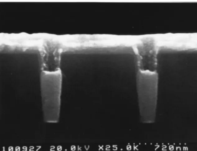
FIG. 8. SEM image of a partially filled 0.18m holes by Cu electroplating. The aspect ratio is 5.5. Applied current density was 60 A/m2.
FIG. 9. XRD peaks of electroplated Cu films. The deposition time is 5 min and applied electrical current densities were 20, 60, and 100 A/m2,
of 1m兲 of electroplated Cu that the resistivity after plating is about 20%–25% higher than the expected resistivity of the metal 共about 1.67m cm兲.4
From AES measurement, the concentration of oxygen in samples with an applied current density of 60 A/m2 was found to be rather low, as shown in Fig. 5. It indicates that the oxidation of Cu in the samples was minimal. Figure 6 shows a SEM image of partially filled 0.45m holes by Cu electroplating. The aspect ratio is 2.3 and applied current density was 60 A/m2. It exhibits an excellent superfilling behavior. Excellent filling behaviors were also found for a dual Damascene structure with a depth as high as 1.5m, as shown in Fig. 7. Moreover, 0.18m vias with an aspect ratio exceeding 5 were filled completely without void or seam. An example is shown in Fig. 8.
Figure 9 shows XRD–2scan peaks of electroplated Cu films on IMP-Cu共125 nm兲/IMP–TaN共30 nm兲 substrates with various applied current densities. The deposition time was 5 min. From XRD analysis, samples deposited with higher cur-rent density exhibited stronger 共111兲 texture. Although higher current density leads to faster deposition rate by Fara-day’s law, it reduces the ability of superfilling. Usually, the applied current is less than 100 A/m2.
IV. CONCLUSIONS
Effects of a new combination of additives in electroplat-ing solution on the properties of Cu thin films have been
investigated. The electroplated Cu films exhibit an excellent superfilling behavior. 0.18 m vias with an aspect ratio ex-ceeding 5 were filled completely without any void or seam. The electrodeposition solution with additives exhibited a lower plating rate. Low resistivity, low porosity, and highly uniform electroplated Cu films were obtained. Strong 共111兲 texture was found for the electroplated Cu films. The resis-tivity of a 450-nm-thick Cu film is 1.84⍀ cm.
ACKNOWLEDGMENT
The work was supported by the Republic of China Na-tional Science Council through Grant Nos. NSC89-2215-E007-006 and NSC89-2215-E110-001.
1C. H. Seah, S. Mridha, and L. H. Chan, Proceedings IEEE International
Interconnect Technology Conference, San Francisco, CA共IEEE,
Piscat-away, NJ, 1998兲, p. 157. 2
P. C. Andricacos, C. Uzoh, J. O. Dukovic, J. Horkans, and H. Deligianni, IBM J. Res. Dev. 42, 567共1998兲.
3L. Arnaud, R. Gonella, G. Tartavel, J. Torres, C. Granelle, Y. Gobil, and Y. Morand, Microelectron. Reliab. 38, 1029共1998兲.
4P. C. Andricacos, Interface共USA兲 Spring , 32 共1999兲. 5
M. E. Gross, C. Lingk, W. L. Brown, and R. Drese, Solid State Technol.
42, 47共August 1999兲.
6L. Oniciu and L. Muresan, J. Appl. Electrochem. 21, 565共1991兲. 7M. A. Alodan and W. H. Smyrl, J. Electrochem. Soc. 145, 957共1998兲. 8
E. D. Eliadis and R. C. Alkire, J. Electrochem. Soc. 145, 1218共1998兲. 9
J. J. Kelly and A. C. West, J. Electrochem. Soc. 145, 3472共1998兲. 10J. J. Kelly, C. Tina, and A. C. West, J. Electrochem. Soc. 146, 2540
共1999兲.
11L. Clark and L. Mursean, J. Appl. Electrochem. 21, 565共1991兲.
1210 Huet al.: Effects of a new combination of additives 1210