CHINESE JOURNAL OF PHYSICS VOL. 36, NO. 1 FEBRUARY 1998
Photoluminescence Studies of GaN Films of Different Buffer Layer and Doping Concentration
C. C. Shen, C. K. Shu, H. C. Lin, J. Ou, W. K. Chen, M. C. Lee, and W. H. Chen
Department of Electrophysics, National Chiao Tung University, Hsinchu, Taiwan 300, R.O.C.
(Received October 23, 1997)
Photoluminescence (PL) measurements of GaN films with various buffer thicknesses and Si-doping concentrations have been carried out. PL response of one specific sample was studied for temperature dependence. The results showed that the band gap energy reduction is linearly proportional to the temperature increase with a slope of - -4 x 10m4 eV.K-’ and that the activation energies for donor-bound and acceptor-bound exciton transitions are 15 and 18 meV, respectively. In Si-doped GaN films, the PL data indicated that the reduced gap depends on the third power of carrier concentration as n1i3. We also obtained a concentration coefficient of 2.34 x 10m4 eV.cm and a band gap energy of 3.426 eV in the undoped GaN film.
PACS. 78.55.-m - Photoluminescence.
PACS. 78.65.-s - Optical properties of thin films. I. Introduction
In recent years, the research on compact and high-power short wavelength light emit-ters, such as light emitting diodes (LEDs) and laser diodes (LDs) in the blue, violet and ultraviolet (UV) g’re ion has been tremendous, especially the gallium nitride (GaN) based materials [l-4]. In spite of the progress in growth methods, there are still substantial questions about physical properties that need to be studied. Photoluminescence (PL) is powerful and sensitive to find defects and impurities, which strongly affect materials prop-erty and device performance. Moreover, the halfwidth of PL peak is a good indication of GaN film quality and crystallinity. In this work, we have carried out PL measurements of GaN films of various buffer thicknesses and %-doping concentrations. The results showed that the band gap energy reduction is linearly proportional to the temperature increase with a slope of N -4 x 10m4 eV.K-l and that the activation energies for donor-bound and acceptor-bound exciton transitions are 15 and 18 meV, respectively [5]. In Si-doped GaN films, the PL data indicated that the reduced gap depends on the third power of carrier concentration as nf I3 [6,7]. We also obtained a concentration coefficient of 2.34 x 10M4 eV.cm, and a band gap energy of 3.426 eV in the undoped GaN film [6,7].
I I . E x p e r i m e n t a l
The undoped and Si-doped GaN epitaxial layers were grown on (0001) sapphire substrate by MOCVD system. The Ga and N sources were trimethylgallium (TMGa) and 32 @ 1998 THE PHYSICAL SOCIETY OF THE REPUBLIC OF CHINA
VOL. 36 C. C. SHEN, C. K. SHU, H. C. LIN, 33
ammonia (NHs). The GaN buffer layer of various thicknesses from 0 to 6OOA were prepared at 525°C prior to epilayer grown on (0001) sapphire at 1025°C. The thickness of the epilayer was about 1.3 pm. For n-type Si-doping, silane (SiH4) diluted with hydrogen was used. The Si-doped GaN films were grown on a 1OOA buffer layer, with carrier concentration ranging from 1.27 x 10¹⁷ cmm3 to 1.29 x 101’ cmp3.
For PI, measurements, a He-Cd laser (325nm, IK Series) was used as the excitation source. The incident light was focused on the sample by a f=7 cm lens. The scattered light was collected by two quartz lenses into a monochromator (ARC SpectroPro-500) with a 1200 lines/mm grating. A shutter and a stepping motor were used to control the exposure time and scan rate. We scanned a range from 330 to 750 nm. The PL detection was made on a liquid nitrogen cooled-charge coupled device (PICCD-576 E) and recorded by a computer with the CSMA software. The spectral resolution was approximately 0.04 nm. Temperature variation was carried out using a closed cycle cryogenic system (APD Cryogenics INC HC-2D) in a range between 10 and 350 K.
III. Results and discussion
Room temperature PL spectra of GaN with various buffer thicknesses are shown in Fig. 1. They all exhibit a band edge (BE) emission of about 3.4 eV. In addition to BE emission, a broad yellow luminescence (YL) b an associated with deep levels occurs aroundd N 2.2 eV (560 nm). Earlier studies showed that the YL is related to the nature of the deep center such as carbon impurity, [l, 2,8] G a vacancy, [9, lo] Ga interstitial, [ll] and N antisite [la]. The weak transitions around 3.2 eV are attributable to N vacancy [13,14].
The full widths at half maximum (FWHMs) of BE and the intensity ratios of BE to YL (Ib/Id ) both show an optimum buffer thickness of about lOOA. This thickness also corresponds to the minimum FWHM of a 258 arcsec in the X-ray diffraction data. Although the sample with SOOA buffer thickness has a narrow PL FWHM of N 60 meV, its X-ray linewidth is broad and the intensity ratio (Ib/Id) is small. We notice that the surface morphology of this sample is very rough and has no hexagonal plate-like hillock pattern like other samples of thinner buffer thickness. We anticipate that more impurities and defects are likely hidden in the rough surface.
At low temperatures and low excitation densities, free carriers can form free exciton states or become bound to impurities so that the luminescence spectra are dominated by these states rather than by band to band recombination. In Fig. 2, we showed the PL spectra of GaN with various buffer thicknesses at 14K. The dominant BE remains at 3.48 eV corresponding to the shallow donor bound exciton (12, D’X) [15]. The spectral shape of this transition is similar to that of the band-to-band transition. In the samples with 100 and 2008, thick buffer, an additional line appeared at 3.435 eV corresponding to the acceptor bound exciton (11, A’X) [15]. S ince A and B bound excitons had been observed with rather narrow linewidths (1.7 meV) by Chen et al. [16] and Smith et al., [17] and our samples have quite high autodoping carrier concentration, these two spectral lines are thus attributed to I2 and 11. However, this 11 transition disappeared in other samples that showed large and broad YL due to more impurities and defects. The 2OOA sample also showed spectral features with phonon replicas between 3.35 and 3.15 eV that are attributable to donor acceptor pair recombination [13]. At lOOA, the highest peak energy occurs at 3.482 eV. A
PHOTOLUMINESCENCE STUDIES OF GaN FILMS OF ‘. VOL.36
1.5 2.0 2.5 3.0 3.5 4.0 1.5 2.0 2.5 3.0 3.5 4.0
Photon energy (eV) Photon energy (eV) FIG.-1. The PL spectra of GaN at room
tem-perature with various buffer thich-nesses. The FWHM and the ratio Ib/Id in the inset show an optimum buffer thickness of about lOOA.
BufferThckness(A)
FIG. 2. The PL spectra of GaN at 14K with various buffer thicknesses. The 12 in-tensity and the ratio I& are shown in the inset.
possible explanation for this peak shift is that the strain within the samples distorts the valence band structure and thus the transition energy [18,19]. From an earlier report, the PL peak of the free exciton without strain is 3.475 eV. The rest of the samples reduced the strain energy by the formation of a network of dislocation at the interface and showed lower blue to yellow intensity ratios [15].
Since the sample with 1OOA buffer thickness showed the largest BE to YL intensity ratio (&,/I,_J) and the strongest Ii and Iz intensities at 14 K, we thus chose this sample by varying its temperature from 14 K to 300 K. Fig. 3 shows the temperature dependent PL spectra near the bandgap. When T < 150 K, the PL spectra are dominated by two peaks with the aid of peak fitting program. One at 3.48 eV is the donor bound exciton (Iz) transition, and the other at 3.446 eV is the acceptor bound exciton (12) transition. At low temperatures (i.e. ICBT << ionization energy) free-to-bound recombination will be dominant in the’PL spectra. At higher temperatures, as more donors are excited into the conduction band, both free-to-bound and band-to-band emissions will occur. Finally, at high enough temperatures, the spectrum will be dominated by band-to-band emission, and deep level emission. As the temperature increases from 14K to 150K, the peak energy of 11 transition increases because the acceptor bound exciton is raised to a higher energy.
VOL. 36 C. C. SHEN, C. K. SHU, H. C. LIN, . 35
However, the disappearance of 12 above T > 150 K is because excitons are thermally excited into the conduction band, so that the transition becomes free to bound. At even higher temperatures, the band edge shrinkage makes Ii decrease with the increasing temperature. We then obtained a linear temperature coefficient of aE,/aT = -4 x 10v4 eV.K-r . It is in the same order of magnitude (from -4 x 10m4 to -6 x 10m4) as those reported by other authors [20]. T he cause of minor differences may be the different electron concentrations and sample quality.
The bound exciton PL intensity as a function of temperature may be given by [al] 1(T) = A/(B + C exp(-&/h,T))
where A, B are constants, C is the transition probability of nonradiative process, and E, is the activation energy. The activation energy is the energy difference between the radiative potential minimum and the intersection of the radiative and nonradiative potential. The thermal fluctuation usually induces transitions to the nonradiative states and consequently reduces the PL intensity. From the function regression of Fig. 3, we obtained the activation energies to be 15 and 18 meV for donor bound and acceptor bound exciton transitions respectively. These activation energies are consistent with the results of Hall measurements by G&z et al. [5].
The band gap energy reduction under heavy doping was illustrated for Si in the work of Wagner (1984) [22]. The theoretical study of Berggren et al. [7] and Abram et al. [6] on the band gap shrinkage in Si doped semiconductors showed an l/3 power variation on the-carrier concentration n. The result is important to device modeling, since the carrier concentration may be high enough to affect the band. One motivation for Wagner’s work was to explain observed discrepancies among data from absorption, PL, and transport measurements. Another was to provide a consistent set of accurate data to compare with theoretical calculations for the reduced gap.
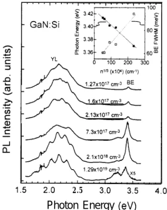
In Fig. 4, we showed the detailed PL spectra of Si-doped GaN. Because the transition rate is proportional to the carrier concentrations, it is clear that the BE emission efficiency increases with the doping concentration, except for the sample with n = 1.29 x 101’ cmm3, which indicates damaged structure. Several small oscillations in YL profile caused by optical interference effects can also be recognized. The appearance of interference effects indicates the smoothness and uniformity of the GaN film surface. Similar to Wagner’s work, [22] the measured PL peak energies of various doping concentrations agreed with the reduced gap that depends on carrier concentration as nII3 In the inset of Fig. 4, the dashed line shows. the theoretical curve of Eg(n1/3) = E,(O) - An1j3, where E,(O) is the bandgap energy in pure semiconductor, and A is the proportionality constant of energy versus n1j3. From this plot, we obtained E,(O) = 3.426 eV and A = 2.34 x 10m4 eVcm. Additionally, the FWHM of Si-doped GaN also increases with the doping concentration roughly as n1i3 that supports the assertion of Berggren et al. [7] and Abram et al. [6]. Since the high impurity concentration strongly broadens the spectral PL response of GaN, transition energies are thus less certain.
36 PHOTOLUMINESCENCE STUDIES OF GaN FILMS OF ‘. VOL. 36 0.0 0.3 06 0.Q I/kBT (N-l) 0 100 200 30( Tempter&we(K) 100ibuff.w 3.3 3.4 3.5 3.6
Photon energy (eV)
3.7
FIG. 3. Ii and 12 emission lines are resolved in the temperature dependent P L
spectra of the lOOA buffer sample. The right inset shows that 12 and Ii are dominant at low temperatures. The left inset shows two bound ex-citons PL intensities as a function of temperature with respective activa-tion energies.
IV. Conlusion
2.5
Photon Energy (eV)
FIG. 4. PL spectra of Si-doped GaN with different concentrations. The inset shows that the band gap energy de-pends on the third power of carrier concentration (n1i3).
Good quality GaN films were grown by MOCVD with different buffer thicknesses. The PL spectrum of 1OOA buffer showed both the best BE FWHM and BE to YL intensity ratio (&,/Id). T hese results are consistent with the DCXRD data. At 14K, we observed the bound exciton energy at 3.48 eV. Samples of other thicknesses showed lower bound exciton energies and low intensity ratios. The peak energy of 12 disappeared at T > 150 K, because donor bound excitons are ionized to the conduction band. Consequently, we obtained a linear temperature coefficient of BE/cYT = -4 x 10m4 eV.K-r, and the activation energies of donor and acceptor bound exciton transitions of 15 and 18 meV, respectively.
PL spectra of the Si-doped GaN showed that BE emission efficiency increases with the doping concentration till 2.1 x 10” cmm3 because the transition rate is proportional to the
VOL.36 C. C. SHEN, C. K. SHU, H. C. LIN, ... 37
carrier concentration. The band gap energy is found to depend on the carrier concentration as a function of n113, and from which we obtained
E,(O) =
3.426 eV andA =
2.34 x lop4 eV.cm.A c k n o w l e d g e m e n t
We are grateful for the support of the National Science Council of Republic of China under contract numbers NSC85-2112-M009-049 and 047.
R e f e r e n c e s
[ 1 ] N. Koide, H. Kato, M. Sassa, S. Yamasaki, K. Manabe, M. Hashimoto, H. Amano, K. Hira-matsu, and I. Akasaki, Cryst. Growth 115, 639 (1991).
[ 2 ] J. I. Pankove, Mater. Res. Sot. Symp. Proc. 162, 515 (1990).
[ 3] S. Nakamura, Y. Harada, and M. Seno, Appl. Phys. Lett. 58, 2021 (1991).
[ 41 S. Krishnankutty, P. Kolbas, M. Khan, and J. Kuznia, J. Elec. Mat. 21, 609 (1992). [ 5 ] W. G&z, N. M. Johnson, C. Chen, H. Liu, C. Kuo, and W. Imler, Appl. Phys. Lett. 6 8 ,
3144 (1996).
[ 6 j R. A. Abram, G. J. Rees, and B. L. H. Wilson, Adv. Phys. 27, 799 (1987). [ 7 ] K. F. Bergg ren, and B. E. Sernelius, Phys. Rev. B24, 1971 (1981).
[ 81 R. Niebuhg, K. Bachem, K. Dombrowski, M. Maier, W. Pletschen, and U. Kaufmann, J. Electronic Materials, 24(11), 1531 (1995).
[. 9-1 X. Zhang, P. Kung, A. Saxler, D. Walker, T. Wang, and M. Rageghi, Acta Phys. Pol. A88, 601 (1995).
[lo] G. C. Yi and B. W. Wessels, Appl. Phys. Lett. 69, 3028 (1996).
[ll] D. M. H o mann, D. Kovalev, G. Steude, B. K. Meyer, A. Hoffmann, L. Eckey, R. Heitz, T.f Detchprom, H. Amano, and I. Akasaki, Phys. Rev. B52, 16 702 (1995).
[12] H. M. Chen, Y. F. Chen, M. C. Lee, and M. S. Feng, Phys. Rev. B56, 11 6942 (1997). [13] B. P. Keller, S. Keller, D. Kapolnek, M. Kato, H. Masui, S. Imagi, U. K. Mishra, and S. P.
Denbaars, Electronics Lett. 31, 1102 (1995).
[14] B. P. Keller, S. Keller, D. Kapolnek, W.-N. Jiang, Y.-F. Wu, H.Masui, X. Wu, B. Heying, J. J. Speck, U. K. Mishra, and S. P. Denbaars, J. of Electronic Materials, 24(11), 1707 (1995). [15] K. Pakula, A. Wysmolek, K. P. Korona, J. M. Baranowski, R. Stepniewski, I. Grzegory,
M. Bockowski, J. Jun, S. Krukowski, M. Wroblewski, and S. Porowski, Solid State Comm. 97(11), 919 (1996).
[16] G. D. Chen, M. Smith, J. Y. Lin, H. X. Jiang, Su-Huai Wei, M. Asif Khan, and C. J. Sun, Appl. Phys. Lett. 68, 2784 (1996).
[17] M. Smith, G. D. Chen, J. Y. Lin, H. X. Jiang, M. Asif Khan, C. J. Sun, Q. Chen, and J. W. Yang, J. Appl. Phys. 79, 7001 (1996).
[18] K. Naniwae, S. Itoh, H. Amano, K. Itoh, K. Hiramatsu, and I. Akasaki, J. of Cryst. Growth 99, 381 (1990).
[19] T. Detchp ro hm, H. Amano, K. Hiramatsu, and I. Akasaki, J. of Cryst. Growth 128. 384 (1993).
[20] H. Teisseyre, P. Perlin, T. Suski, I. Grzegory, S. Porowski, J. Jun, A. Pietraszko, and T. D. Moustakas, J. Appl. Phys. 76(4), 2429 (1994).
[21] S. Mochizuki and K. Umezawa, J. Phy. : Condens. Matter 8, 7509 (1996). [22] J. Wagner, Phys. Rev. B29, 2002 (1984).