利用 MOCVD 製備高介電閘極材料之研究
計劃編號: NSC-90-2215-E-009-117
執行期間: 90/8/1~91/7/31
主持人:趙天生 交通大學電子物理系 教授
E- mail: [email protected]
IntroductionFor standard SiO2or SiON gate insulators with thickness <1.5 nm, leakage currents will become prohibitive in a number of the applications of complementary metal-oxide semiconductor technology.1 Thus, to improve reliability and reduce power consumption, there is a worldwide search for a replacement for these gate dielectrics having a higher dielectric constant, κ. Recent attention has focused on the silicates of those transition or rare -earth metals that are thermodynamically stable on silicon in the sense that their oxides will not be reduced by silicon to form metal or silicide layers. Zirconium silicate films have been shown to be promising candidates for a replacement gate insulator in deep-submicron CMOS technology but a production-worthy deposition technique still needs to be found. One such technique is metal-organic chemical vapour depositon (MOCVD). In MOCVD, alkoxide and ß-diketonate precursors are commonly used. However, the former are air- and moisture-sensitive. The ß-diketonates are less ambient sensitive, and have higher thermal stability requiring higher deposition temperatures. The films can exhibit severe carbon contamination or, for the ß-diketonates with fluorine-containing ligands, fluorine contamination. In order to combine the advantages of alkoxides and ß-diketonates, mixed ligand Zr and Si precursors were developed to lower the thermal stability but
maintain a higher ambient stability and higher volatility.
In this work, ultra-thin Zr silicate films were deposited on Si(100) using mixed alkoxide
β-diketonate precursors2. Zr(Oi-Pr)2(thd)2 and Si(Ot-Bu)2(thd)2 dissolved in octane were introduced into the reactor with a liquid -injection
system. O2 or NO were introduced into the
chamber separately to reduce C contamination in the films. The C concentration was further reduced by using a “pulse-mode” deposition in which the precursors and the oxidant were introduced during separate steps. Analysis by X-ray Photoelectron Spectroscopy (XPS) has shown that using this pulse-mode technique both NO and O2 reduce the carbon contamination in the films effectively. The zirconium silicate films have been analyzed by high-resolution transmission electron microscopy (HRTEM), atomic force microscopy (AFM), x-ray photoelectron spectroscopy (XPS), and medium energy ion scattering (MEIS). The effects of post deposition anneals were investigated. The current density versus voltage (J-V) characteristics and capacitance versus voltage (C-V) characteristics were analysed for Al-gated capacitors.
Result and Discussion
Fig. 1 shows the XPS Zr3d and C1s spectra for a Zr0.5Si0.5O2 film deposited using NO. No evidence of C-Si, Zr-C and Zr-Si bonds were found in the spectra of the optimized films.
HRTEM images show that the as -deposited Zr silicate films and the interfacial layers are amorphous (Fig. 2).
Nitric oxide forms an oxynitride buffer layer which retards oxygen diffusion to the Si interface, thus minimizing the thickness of the interfacial layer. The thinnest interfacial layers for the as-deposited films were 0.6 nm determined by HRTEM (see Fig. 2) or 0.3 nm determined by medium energy ion-scattering (MEIS). After post deposition anneals at 850 ºC Zr silicate films with the composition Zr0.5Si0.5O2 and their interfacial layers were still amorphous and no phase separation was observed. The Zr concentration in the interfacial layer was below the sensitivity of the MEIS technique (~ 5 at.%) before and after annealing and this has been confirmed by EELS analysis.
The films were annealed in O2 to remove
surface carbon contamination from unreacted precursor on the surface of the film and improve the electrical quality of the interface layer. A
“spike anneal in O2 at 850 ºC increased the
thickness of the interfacial layer.
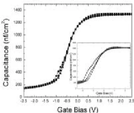
Fig. 3a shows the MEIS spectrum for the as-deposited film. The C, N, and O peaks for pieces of the same wafer before and after a spike anneal in O2 at 850 ºC is shown in Fig. 3b. The most important change in the MEIS spectra is observed in the broadening of the O peak on the low energy side. The simulation indicates that the interfacial layer increased to a thickness of 0.9 nm. The Zr silicate films described in this work exhibit promising C-V (Fig. 4) and J-V (Fig. 5) characteristics. The hysteresis, fixed charge density and the effective density of trapped charge at the interface were improved significantly by anneals at 850 ºC (Fig. 6). Most of the
frequency-dependent interface states, not passivated by the low temperature FGA, were eliminated after the 60 s nitrogen anneal at 850 ºC (Fig. 7). After a spike anneal in O2 at 850 ºC and an anneal for 60 s in N2 at 850ºC, a Zr silicate film with an equivalent oxide thickness (EOT) of 2.3 nm has exhibited a leakage current about 20 times lower than that of a SiO2 film with the same EOT.
In this study ultra -thin Zr silicate films were deposited on Si(100) using Zr(Oi-Pr)2(thd)2 and Si(Ot-Bu)2(thd)2 dissolved in octane. Either O2 or NO was used as the oxidizing gas. One of the functions of the O2 anneal was to eliminate the C from precursor evidently left on the surface of the film. The fact that this remaining precursor was not oxidized during the final oxidation stage in the deposition chamber suggests that the decomposition of the precursor is a rather complicated process requiring both a separate oxidant and species produced during the succeeding precursor pulse.In the precursors used for the Zr silicate deposition the Zr and Si are co-ordinated to six O atoms, while only two are required to form the silicates. This leaves 4 oxygen atoms per molecule that may release active oxygen during the decomposition of the precursor. The ultra-thin Zr silicate films described in this work exhibit promising C-V and J-V characteristics.
Conclusion
These electrical properties demonstrate that a thin Zr silicate film formed by Zr(Oi-Pr)2(thd)2, Si(Ot-Bu)2(thd)2 and nitric oxide might be a promising gate dielectric for deep submicron CMOS devices, if ways can be found to decrease the interface layer thickness.
References
1. G.D. Wilk, R.M. Wallace and J.M. Anthony, J.
Appl. Phys. 89, 5243 (2001).
2. A.C. Jones, Chem. Vap. Deposition, 4, 169 (1998).
190 188 186 184 182 180
Zr 3d
Intensity (a.u.)
Binding Energy (eV)
290 288 286 284 282
C 1s
Intensity (a.u.)
Binding Energy (eV)
Figure. 1. XPS spectra with background subtracted showing
data (,,,), fitted peaks (- - -), and sum of fitted peaks (−) for
the as-deposited Zr0.5Si0.5O2 film .
Figure. 2. HRTEM cross section of as-deposited Zr0.5Si0.5O2
film.
Figure3 (a) MEIS spectrum of 2.7 nm thick as-deposited Zr
silicate film with a Si:Zr ratio of 1.3:1: (,,,) data, (−)
simulation. (b) C, N, and O peaks for the as-deposited Zr silicate film with a Si:Zr ratio of 1.3:1 of Fig. 3a before
and after spike anneal in O2 at 850 ºC: (,,,) before
anneal, (−) simulation, (777) after anneal, (---)
simulation.
Figure4. High frequency C-V characteristics of capacitors with Zr silicate gate dielectric obtained at 100 kHz. The
samples were spike annealed in O2 at 850 ºC (!!!), spike
annealed in O2 at 850 ºC and FGA at 380 ºC for 20 min (,,,),
spike annealed in O2 at 850 ºC, then annealed in N2 at 850 ºC
for 60 s and FGA at 380 ºC for 20 min(777). The equivalent
oxide thicknesses are 2.3, 2.22, and 2.32 nm, respectively.
Zr silicate
Si
Figure 5. Current density as a function of gate voltage for the Zr silicate film of Fig. 6 with for substrate injection:
as-deposited (777), after a spike anneal at 850 ºC in O2 and a
FGA at 380 ºC for 20 min (◆◆◆), after only a spike anneal
at 850 ºC in O2 (★★★), after a spike anneal at 850 ºC in O2,
followed by a nitrogen anneal at 850 ºC for 60 s and a FGA at
380 ºC for 20 min (!!!).
Figure 6. The effect of different post deposition anneals for
Zr silicate films on (a) the flatband voltage shift, ΔVFB, (b) the
fixed charge density, Nf , and the effective density of trapped
charge at the interfaceΔNt . The spike anneal was done in O2 at
850 ºC. The FGA is a forming gas anneal at 380 ºC for 20 min.
The N2 anneal was done at 850 ºC for 60 s.
Figure7. Frequency dependence of the C-V characteristics of the Zr silicate film which has an EOT of 2.32 nm after a
spike anneal at 850 ºC in O2, followed by a nitrogen anneal at
850 ºC for 60 s and a FGA at 380 ºC for 20 min: 10 kHz (!!!),
100 kHz (,,,), and 1 MHz (777). A slight frequency dispersion
is evident below midgap, indicating the existence of donor-like interface states. The inset shows the frequency dispersion of
the sample after a spike anneal at 850 ºC in O2 and a FGA at