國
立
交
通
大
學
電機學院微電子奈米科技產業研發碩士班
碩
士
論
文
寬通道側向電流效應之研究
與新穎薄膜電晶體結構之開發
研 究 生:趙育晟
指導教授:張國明 教授
中 華 民 國 九 十 六 年 六 月
寬通道側向電流效應之研究
與新穎薄膜電晶體結構之開發
研 究 生:趙育晟 Student:Yu-Cheng Zhao
指導教授:張國明 博士 Advisor:Dr. Kow-Ming Chang
國 立 交 通 大 學
電機學院微電子奈米科技產業研發碩士班
碩 士 論 文
A Thesis
Submitted to College of Electrical and Computer Engineering National Chiao Tung University
in partial Fulfillment of the Requirements for the Degree of
Master in
Industrial Technology R & D Master Program on Microelectronics and Nano Sciences
June 2007
Hsinchu, Taiwan, Republic of China
中華民國九十六年六月
寬通道側向電流效應之研究
與新穎薄膜電晶體結構之開發
學生:趙育晟
指導教授:張國明
國立交通大學資訊科學系﹙研究所﹚碩士班
摘
要
這篇論文中,第一次討論到寬通道薄膜電晶體的飽和電流和寬通道調變在線性 變化區的關係.我們發現當通道寬度大於汲極源極寬度時,寬通道測向電流效應將產 生.這個效應將在較寬的通道產生新的電流路徑和較低的總電阻使的飽和電流上升. 當通道的寬度漸漸增加時,飽和電流一開始會跟著通道的寬度增加而增加.然後 到達某個定值後就跟通道的寬度增加無關.當通道的寬度大於有效的通道寬度時,飽和 電流增加到最大值時.最大的飽和電流和通道長度汲極源極寬度有某種關係.我們發現 飽和電流的增加比率和通道長度除以汲極源極寬度的值成正比隨著通道寬度的增加而 增加.
The study of the side-channel current effect of wide channel
width and the fabrications of the novel Poly-Si thin-film
transistor structure
student:Yu-Cheng Zhao
Advisors:
Dr. Kow-Ming Chang
Department﹙Institute﹚of Electrical Engineering and Computer Science
National Chiao Tung University
ABSTRACT
In this paper, it is first time to discuss the ON-state drain current of a special TFT structure with a wider channel width and a narrower source/drain width in the linear region. We found that, when the channel width is wider than that of the source/drain, the side channel current effect (SCCE) would be generated, and this effect would cause the increase of the ON-state drain current due to the additional current flow paths existed in the side channel regions and lower channel resistance. As the side channel width increasing, the ON-state drain current would be initially increased and then gradually independent of the side channel width when the side channel width is larger than the effective side channel. The maximum ON-state drain current will apply to channel length and source/drain width. We also found that the ON-state drain current gain would be directly proportional to the channel length and the channel length to source/drain width ratio, and dependent on the side channel width.
誌
謝
能完成這篇論文,首先要感謝的是張國明老師讓我有機會參
加這計畫的研究,再來要感謝林俊銘學長對此論文完善的規劃,以
及提供的意見和想法.還有數據分析上面的指導,才能完成此篇問
文.感謝畢業的學長們,在機台上面的指導,還有討論論文時提供
很多關於薄膜電機體相關的研究資料最後感謝在實驗過程中,給
予指導的機台工程師跟其他同學的經驗分享.才能讓實驗順利的
完成.感謝在實驗時能一起渡過那段時光的同學們.大家的互相鼓
勵跟支持幫助我很多.讓我能有用勇氣完成此論文.謝謝曾經給過
我幫助的大家,這是我完成論文最大的動力.
Contents
Chapter 1 Introduction
1.1 Overview of Low Temperature Poly-Si TFTs……….8
1.2 Issues in Low Temperature Poly-Si TFTs……….9
1.3 Motivation………9
1.4 Thesis Organization………...10
Chapter 2
Effect of Channel Width Widening on a Poly-Si Thin-Film
Transistor Structure in the linear region
2.1
Abstract………12
2.2 Device
fabrication……….12
2.3 The Simulation
Results……….15
2.4. Equivalent Circuit of the Channel Region in the Test Structure
(W
BchB>W
BsdB) in the linear region……….15
2.5 Electrical Characteristics of the Test Structure(W
BchB>W
BsdB)………16
2.6 Relationship of the ON-state drain current Gain with the Channel Length,
the Side Channel Width and the Source/Drain Width for long source/drain
width (W
BsdB= 5 µm and W
BsdB= 10µm)……….18
2.7 Relationship of the ON-state drain current Gain with the Channel Length,
the Side Channel Width and the Source/Drain Width for short
source/drain width (W
BsdB= 1 µm and W
BsdB= 2 µm)……….19
Chapter 3
Effect of channel width widening on a poly-Si TFT structure with a
half side channel region in the linear region
3.1 abstract………22
3.2 Device fabrication………22
3.3 Electrical Characteristics of the Test Structure………..24
References………26
Figure captions………29
Chapter 1
Introduction
1.1 Overview of Low Temperature Poly-Si TFTs
Polycrystalline silicon thin-film transistors (poly-Si TFTs) have been intensively studied for application to high performance large-area active matrix liquid-crystal display (AMLCD) systems [1], [2]. They are commonly used in active-matrix liquid-crystal displays (AMLCDs) [3], [4] as pixel switches, drivers, and peripheral control circuits. In recent years, a lot of efforts have been put forth to improve the material quality and device structure of poly-Si TFTs to obtain better device performance. poly-Si TFTs have attracted much attention due to the possibility of realizing the integration of driving circuits and pixel elements on one glass substrate, and the potential to accomplish the system-on-panel (SOP) . High-performance poly-Si TFTs are required for this goal. In generally, poly-Si TFTs have two structures: top-gate coplanar structure and bottom-gate structure. The top-gate TFTs are mainly used in AMLCD application because their self-aligned source/drain regions provide low parasitic capacitances and are suitable for device scaling down. On the other hand, Bottom-gate TFTs have better interface and higher plasma hydrogenation rate than top-gate TFTs, but they have lower current and need extra process steps for backside exposure and difficult fabrication
Recrystallization technology is important for low temperature Poly-Si TFTs because of the grain size, grain boundary and intragranular defects [5], which influence the performance of Poly-Si TFTs. To achieve the large grain size, high performance and low temperature process, several recrystallization technologies have been proposed: solid phase crystallization (SPC) [6], eximer laser annealing (ELA) [7]−[9], and metal-induced lateral crystallization (MILC) [10] − [12] etc. In this paper, we use SPC to recrystallize the poly-Si TFTs.
The major advantages of applying poly-Si TFTs on AMLCDs are large carrier mobility and low photocurrent and high reliability. In poly-Si film, carrier mobility larger than 100 cmP
2
The dominant leakage current mechanism in poly-Si TFTs is the field emission via the grain boundary traps by a high electric field near the drain. Therefore, reducing the lateral electric field near the drain junction is needed. For example, using a lightly doping drain structure can reduced the lateral electric field. The LDD structure certainly not only reduces the electric field but also enhances source/drain series resistance that limits the on-state current.
1.2 Issues in Low Temperature Poly-Si TFTs
Although the poly-Si TFTs were used to instead of the amorphous TFTs for the high mobility, the complex grain structure in poly-Si has a strong influence on device characteristics. Large amount of defects serving as trap states locate in the disordered grain boundary regions. These traps also cause the valence-band carriers to jump to conduction-band via trap-assisted thermionic emission or trap-assisted thermionic field emission, leading to large leakage current. It is well known that there are three kinds of the leakage current mechanisms in poly-Si TFTs .First, when the drain voltage is very low, the leakage current is governed by thermally generated carriers via the trap states. The leakage current therefore is dependent on the drain voltage, but independent of the gate voltage. Second, when the drain voltage is in the intermediate range, the leakage current is generated by the thermionic field emission of electrons indicated. In this case, the electrons in the valence-band are thermally excited to the trap states, and then tunnel to the conduction-band quantum mechanically. The leakage current therefore increases with increasing the gate voltage due to the narrowing of the barrier width. Third, when the gate voltage is high enough, the leakage current is governed by the field enhanced tunneling. Obviously, decreasing the drain electric field is helpful to reduce the leakage current.
Therefore, the poly-Si TFTs suffer from the high leakage current in the OFF-state and the kink effect in the ON-state [14]. The surface roughness of poly-Si film will enhance the local electrical field near the interface between gate oxide and channel, which will also degrade the reliability of TFT under high gate bias operation. However, LDD structure indeed reduces the electric field [15] but also causes high source/drain series resistance which limits the on-state current. Besides, an extra mask in LDD structures is a major problem [16], [17].
Besides, under the long-term operation, the stability of the poly-Si TFTs is a major issue. The hot carrier effect is also an important reliability in LTPS TFTs.
1.3 Motivation
Poly-Si TFTs can be used to integrate peripheral driver circuits on glass for system integration. In order to integrate peripheral driving circuits on the same glass substrate, both a large current drive and a high drain breakdown voltage are necessary for poly-Si TFT device characteristics. It has been previously reported that the use of a thinner active channel film is beneficial for obtaining a higher current drive [18], [19]. However, the use of thin active channel layer inevitably results in poor source/drain contact and large parasitic series resistance.
To achieve this ideal TFT structure, we have proposed a novel four-mask step TFT structure with self-aligned raised source/drain (SARSD) [20]. In SARSD TFT structure, a special structure with a wider channel width and a narrow source/drain width is formed. It also reported that a higher ON-state drain current would be obtained due to lower series resistance and additional current flow paths existing in the side-channel regions [20]. To explain the behavior of the ON-state drain currents of the Poly-Si TFT’s and to simulate these ON-state drain current values, several models have been proposed [21]-[24]. The relationship of the ON-state drain current of the structure with a wider channel width and a narrower source/drain width on the channel width, the channel length and the source/drain width must be defined clearly. This is the motive of our study on the wider channel width effect in Poly-Si TFTs. We hope that this study would help those skilled in this art to further understand the behavior of the carrier transport in the channel region when the channel width is larger than the source/drain width and would explain the increase of the ON-state current of the wider channel width TFT structure, such as the SARSD TFT structure.
In this paper, we used a test structure with a wider channel width and a narrower source/drain width to study the influences of the channel width, the channel length and the source/drain width on the ON-state drain current. Because the kink effect would cause an anomalous current increase in the saturation region, we only focused on the ON-state drain current in the linear region in this paper.
1.4 Thesis Organization
In chapter 1, a brief overview of LTPS TFT technology and related applications were introduced.
region will be discussed.
In chapter 3, the effect of channel width widening on a poly-Si TFT structure with a half side channel region in the linear region will be discussed.
Chapter 2
Effect of Channel Width Widening on a Poly-Si
Thin-Film Transistor Structure in the linear region
2.1 Abstract
In this study, it is first time to discuss the ON-state drain current of a special TFT structure with a wide channel width and narrow source/drain width in the linear region. When the channel width is wider than that of the source/drain width, the ON-state drain current of the special TFT structure with a wide channel width and narrow source/drain width will be increased due to the additional current flow paths existing in the side channel regions and low channel resistance. As the side channel width increased, the ON-state drain current will initially increase and then gradually become independent of the side channel width. The ON-state drain current gain is proportional to the ratio of channel length to source/drain width.
It also has been reported that a higher ON-state drain current would be obtained due to lower series resistance and additional current flow paths existing in the side-channel regions [22]. There are some articles discussed with the case of the narrow channel width [23]-[26], but there are no any articles discussed with the variations of the channel width which is larger than the source/drain width.
Therefore, before new physical models are proposed to explain and simulate the ON-state drain current of the structure with a wider channel width and a narrower source/drain width, the relationship of the ON-state drain current of the structure with a wider channel width and a narrower source/drain width on the channel width, the channel length and the source/drain width must be defined clearly.
In this paper, we used a test structure with a wider channel width and a narrow source/drain width to study the influences of the channel width, the channel length and the source/drain width on the ON-state drain current. Because the kink effect would cause an anomalous current increase in the saturation region, we only focused on the ON-state drain current in the linear region in this paper.
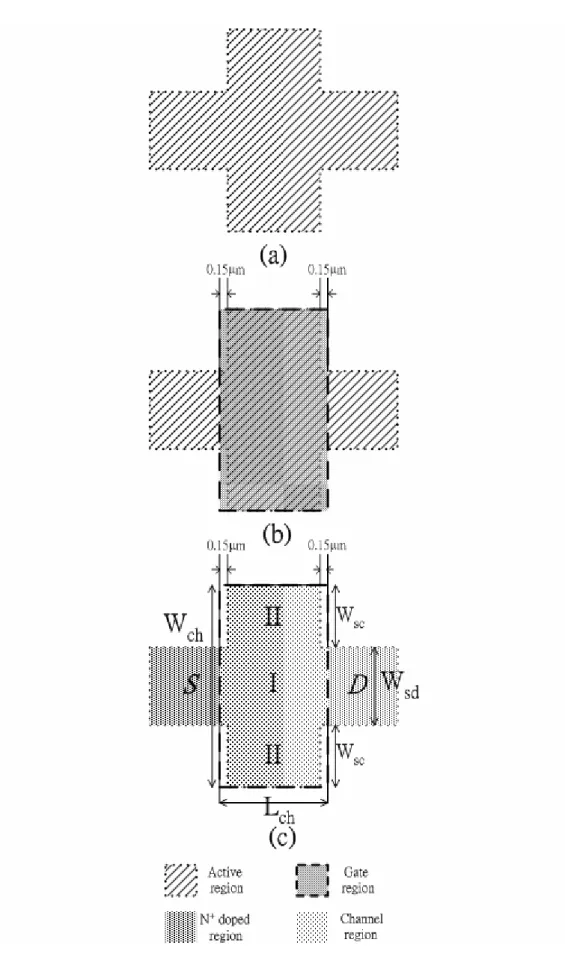
The fabrication processes of the tested n-channel poly-Si TFT with a wider channel width and a narrower source/drain width were as follows: A 50-nm thick α-Si layer for active region was deposited by low pressure chemical vapor deposition (LPCVD) system using SiHB4B at 550°C on 500-nm thermal oxidized silicon wafers, then 600°C 24 hr anneal (SPC). The active region was patterned by G-line stepper and was formed using reactive ion etching (RIE), as shown in Figure 2.1(a). A 50-nm low pressure chemical vapor deposition (LPCVD) TEOS gate oxide layer was deposited, and then a 300-nm LPCVD poly was deposited which was patterned by G-line stepper and was formed using reactive ion etching (RIE). G-line stepper system has a layer-to-layer misalignment, which is less than 0.15 µm, the gate region, as shown in Figure 1(b), having two overlapping regions that lengths are 0.15 µm to ensure that the source/drain width would be narrower than the channel width. After the gate region formation, Gate, Source and Drain regions were formed by ion implantation of PhosphorousP P
(Dose = 5 x 10P 15
PcmP -2
P at 30 keV) and then activated in nitrogen ambient at 600 °C for 24 h, as shown in Figure 1(c). After the source, drain and gate activation, the 500-nm passivation oxide was deposited by PECVD. Wet etching opened contact holes. A layer of aluminum was then deposited by thermal coater system with a thickness of 500 nm. After metal patterning, an annealing process with forming gas l is performed at 400°C for 30 min.
The detailed fabrication process flows are listed as follow: 1. (100) orientation Si wafer
2. Initial cleaning
3. Thermal wet oxidation at 980°C to grow 500nm thermal SiOB2B in furnace 4. 500nm a-Si were deposited by LPCVD at 620°C
5. SPC crystallization for 24 hours 6. pattern # 1: define active regions 7. Poly-Si dry etch by TCP system
8. 50nm TEOS oxide deposition by LPCVD
9. 300nm poly-Si was deposited by LPCVD at 620°C in SiHB4B gas 10. pattern # 2: define poly gate region
11. Poly-Si dry etch by TCP system 12. Ion implantation: PP 31 P, 5×10P 15 P cmP -2 P, 30 KeV
14. 400 nm TEOS oxide film was deposited by LPCVD for the passivation 15. pattern # 4: Open contact holes
16. Wet etching by B.O.E
17. 500nm Al thermal evaporation 18. Mask # 4: define metal pad
19. Etching Al and removing photoresist
20. Al sintering at 400°C in NB2B ambient for 30 minutes
(pattern # 1: define active regions)
(pattern # 2: define poly gate region)
and two side channel regions (region II). The channel length and width are represented as LBchB and WBchB, respectively. The channel width (WBchB) is wider than the source/drain width (WBsdB), and the channel width can be written as
W =W
+2W =W +2W
ch
mc
sc
sd
sc
(1) where WBscB is the width of the side channel region ( Figure 1(c)) in the test structure and WBmcB is the main channel width that is equal to source/drain width (WBsdB).For comparison, the conventional poly-Si TFT’s structure which the channel width is identical to the source/drain width was also fabricated at the same time.
2.3 The Simulation Results
We discussed the simulation results of the Test Structure ( WBchB > WBsdB) and the Conventional Structure ( WBchB = WBsdB).In order to simulate the current flows of the test and the conventional structures, the 2-D numerical simulator MEDICI was used [27]. Figure 2.2 shows the simulated current flow lines of the conventional structure in ON-state. The channel length and the channel width of the simulated conventional structure are 10 µm and 5 µm, respectively.
Comparing Figures 2.2(b) with 2.2(c), it can be observed that additional current flow generated in the side channel regions and the current flow line in the side channel regions would be increased with increasing the channel length (LBch B= 3 µm to LBchB = 10 µm). It indicates that the current flow distribution in the side channel regions would be dependent on the channel length.
Then comparing with Figures 2.2(c) and 2.2(d), even increasing the source /drain width (WBsd B= 5 µm to WBsdB = 10 µm), the distribution and the effective distribution width of current flow lines of WBsdB = 10 µm in region II are almost identical to those of WBsd B= 5 µm. It indicates that an increase of the source/drain width (or main channel width) would not significantly change the distribution of current flow lines in side channel.
2.4. Equivalent Circuit of the Channel Region in the Test
Structure( W
BchB> W
Bsd B) in the linear region
To explain the additional current flow paths of the test structure in the side channel regions, we used the equivalent circuit as shown in Figure 2.3. In the side channel regions of the Figure 2.3, the resistance of path 2 (RBsc2B) would be larger than that of path 1 (RBsc1B) due to
the distance of path 2 is longer than path 1. So, the currents flow via the path 2 must be less than the currents flow via the path 1. According to this equivalent circuit, the total channel resistance (RBtotB) of the test structure could be written as:
1 R = < R tot 1 2 2 mc + + +... R R R mc sc1 sc2
(2)
andL
ch
R
=
mc W
C
(V -V )
sd eff ox gs th
µ
(3)
where RBmcB is the resistance of the main channel region in the linear region, and RBmcB is also the channel resistance of the conventional structure in the linear region. The total channel resistance (RBtotB) of the test structure should be smaller than that of the main channel region (RBmcB). Therefore, the ON-state drain current of the test structure would be higher than that of the conventional structure. As discussed above, the ON-state drain current of the test structure would be saturated at a certain value, if WBscB were large enough.2.5 Electrical Characteristics of the Test Structure ( W
BchB> W
BsdB)
In order to confirm our observations on the results of Figures 2.2 and 2.3, the experimental data of the test structure were shown in Figures 2.4 - 2.6.In Figure 2.4(a), the IBdsB-VBgsB transfer characteristics of the test structure with different side channel widths. It can be observed that the on-state drain currents of the test structures are higher than conventional structure. The ON-state drain current of the test structure would be initially increased with increasing the side channel width (WBscB), and then gradually independent of WBscB, even though the WBsdB / LBchB ratio of the test structure was changed from 10 µm /5 µm to 5 µm /15 µm
In Figure 2.5(a). These results are corresponding with our suggestions in the section 2.3. In the Figures 2.4(b) and 2.5(b), the characteristics of the test structure with different side channel widths were shown. In the Figures 2.4(b) and 2.5(b), the ON-state drain currents of the test structure are larger than those of the conventional structure. It can be observed that increasing Wsc will reduce the channel resistance. According to the results of Figure 2.4, Figure 2.5 and the equation (1), it can be observed that the reason of higher ON-state drain
current of the test structure is lower channel resistance.
Figure 2.6 shows the ON-state drain current distributions of the test structure with the varied side channel width for different channel lengths. Ten test TFTs were measured for each condition. In Figure 2.6, it can be observed that the ON-state drain current of the test structure would be initially increased with increasing WBscB, and then gradually be saturated in certain WBscB. This special side channel width would be called as the effective side channel width (WBsc,effB). The higher ON-state drain current would be obtained by increasing channel width (WBsc).B In Figures 2.4 and 2.5, it can be observed that the value of the effective side channel width (WBsc,effB) would be decreased with decreasing the channel length. It is consistent with the simulated results of Figure 2.2.
In order to analyze the increased ratio of the ON-state drain current caused by increasing channel width (WBsc). B The average values of the ON-state drain current gain (ABiB) with different channel width (WBsc)B were shown in Figures 2.7(a) and 2.7(b). The ON-state drain current gain (ABiB) is defined as I I ds,t ds,c A i I ds,c − ≡
(4)
where IBds,cB is the ON-state drain current of the conventional structure; IBds,tB is the ON-state drain current of the test structure with different side channel widths.
In Figures 2.7(a) ~2.7(f), it can be observed that the average values of the ON-state drain current gain (ABiB) of the test structure would be increased as increasing the channel length. In addition, in the same channel length (such as LBchB = 15 µm), the effective side channel widths (WBsc,effB) of WBsd B= 5 µm and WBsd B= 10 µm are almost the same. These results are consistent with the simulated results of Figures 2, and the decrease of the WBsdB from 10 µm to 5 µm would increase the average value of ABiB. From the results of Figures 2.5 and 2.6, we can conclude that the effective side channel width (WBsc,effB) is dependent on the channel length (LBchB) and independent of the source/drain width (WBsdB), and the effective side channel width (WBsc,effB) would be not only dependent on the side channel width, but also dependent on the channel length and the source/drain width.
2.6 Relationship of the ON-state drain current Gain with the
Channel Length, the Side Channel Width and the Source/Drain
Width for long source/drain width (W
BsdB= 5
µm and W
BsdB= 10
µm)
To investigate the relationship of the ON-state drain current gain (ABiB) with the channel length, the side channel width and the source/drain width, the distributions of the ON-state drain current gain (ABiB) against LBchB and LBchB/ WBsdB ratio with different channel widths and side channel width conditions were shown in Figures 2.8(a)-2.8(b) and Figures 2.9(a)-2.9(b). As shown in Figures 2.8(a) and 2.8(b), it can be observed that the ON state current gains ABiB were directly proportional to LBchB for both WBsdB = 5 µm and 10 µm. In Figures 2.9(a) and 2.9(b), it can be also observed that the ON state current gains ABiB were directly proportional to the LBchB/ WBsdB ratio for both WBsdB = 5 µm and 10 µm. Therefore, we can conclude that the ON state current gain is directly proportional to LBchB and the LBchB/ WBsdB ratio, and is dependent on WBscB.
In Figures 2.8 and 2.9, the relationship of the ON-state drain current gain (ABiB) with the channel length LBch Band the source/drain width WBsdB for long the source/drain width can be written as:
L
C
ch
A
B
i
W
sd
+
≅
(5)
Where B and C are constants.
When WBscB ≥
W
Bsc,effB , B is about 0.48 according to Figures 2.9 ; and C is about -1.55 in Figures 2.8.Combining the equations (4) and (5), the maximum ON-state drain current gain (ABi,maxB) is obtained:
I
I
L -1.55
ds,t,max
ds,c
ch
A
0.48(
)
i,max
I
W
ds,c
sd
−
≡
≅
(6)
Because Eq. (6) is derived from the experimental data of, WBscB ≥ WBsc,effB ., the maximum ON-state drain current of the test structure (IBds,t,maxB) can be written as:
L -1.55
ch
I
[1 0.48(
)]I
ds,t,max
W
ds,c
sd
≅ +
(7)
Figure 2.10, the calculated data almost agreed with the experimental data for different source/drain widths and different applied drain biases ( VBdsB = 5 V or 10 V).
In Figures 2.8(a) and 2.9(a), WBscB is 6 µm which is smaller than the effective side channel width (WBsc,effB) of the test structure of LBchB = 15 µm. WBsc,effB of the test structure of LBchB = 15 µm is about 10 µm as shown in Figure 2.7. Therefore, the experimental data of (LBchB = 15 µm ,WBscB =6 µm) can not be fitted by Eq. (5) .
In Figures 2.8(b) and 2.9(b), they were not fitted by Eq. (5), even though WBscB(= 14 µm) is larger than WBsc,eff B(~ 10 µm). The channel resistance is directly proportional to the LBchB/WBsdB ratio. Larger LBchB/WBsdB ratio represents larger channel resistance. The main reason of the experimental data of LBchB/WBsdB = 15 µm/ 5 µm were not fitted by equation(5). In Figures 2.8(b) and 2.9(b) is that larger channel resistance is dominant.
When the channel width is wider than the source/drain width, the side channel would cause the increase of the ON-state drain current due to the additional current flow paths existed in the side channel regions and lower channel resistance. As the side channel width (WBscB) increasing, the ON-state drain current would be initially increased and then gradually independent of the side channel width when the side channel width is larger than the effective side channel width (WBsc,effB). We also found that the ON-state drain current gain would be directly proportional to the channel length and the channel length to source/drain width ratio, and dependent on the side channel width. Moreover, once the channel length to source/drain width ratio is too large, higher channel resistance caused by larger channel length to source/drain width ratio would suppress the effect and limit the increase of the ON-state drain current gain.
2.7 Relationship of the ON-state drain current Gain with the Channel
Length, the Side Channel Width and the Source/Drain Width for short
source/drain width (W
BsdB= 1
µm and W
BsdB= 2
µm)
In Figures 2.11 and 2.12, the relationship of the ON-state drain current gain (ABiB) with the channel length LBch Band the source/drain width WBsdB for short source/drain width can be written as:
L
C
ch
A
B
i
W
sd
+
≅
(5)2.7(a) For W
BsdB= 1
µm
When WBscB ≥ WBsc,effB , B is about 0.34 according to the slopes of the auxiliary straight lines in Figures 2.11(a) and 2.11(b); and C is about zero in Figures 2.12(a) and 2.12(b).
Combining the equations (4) and (5), the maximum ON-state drain current gain (ABi,maxB) is obtained:
I
I
L
ds,t,max
ds,c
ch
A
0.34(
)
i,max
I
W
ds,c
sd
−
≡
≅
(8)
In the case of WBscB ≥ WBsc.effB, if the channel length and the source/drain width are determined, the saturated or maximum ON-state drain current of the test structure (IBds,t,maxB) can be written as:
L ch I [1 0.34( )]I ds,t,max W ds,c sd ≅ +
(9)
In Figure 2.13 presents experimental data and calculated data. The calculated data roughly agreed with experimental data for different source/drain widths and different applied drain biases ( VBdsB = 5 V or 10 V) (Fig. 2.13).
2.7(b) For W
BsdB= 2
µm
When WBscB ≥ WBsc,effB , B is about 0.42 according to the slopes of the auxiliary straight lines in Figures 2.11(a) and 2.11(b); and C is about zero in Figures 2.12(a) and 2.12(b).
Combining the equations (2) and (3), the maximum ON-state drain current gain (ABi,maxB) is obtained: For WBsdB = 2 µm I I L ds,t,max ds,c ch A 0.42( ) i,max I W ds,c sd − ≡ ≅
(10)
determined, the saturated or maximum ON-state drain current of the test structure (IBds,t,maxB) can be written as:
For WBsdB = 2 µm
L
ch
I
[1 0.42(
)]I
ds,t,max
W
ds,c
sd
≅ +
(11)
In Figure 2.13 presents experimental data and calculated data. The calculated data roughly agreed with experimental data for different source/drain widths and different applied drain biases ( VBdsB = 5 V or 10 V) (Fig. 2.13).
2.8 Conclusion
In this chapter, we discussed the ON-state drain current of a structure with wide channel width and narrow source/drain width. We found that the On-state drain current of this special structure would be larger than which of the conventional structure (the channel width is identical to the source/drain width), due to the additional current flow paths and low channel resistance. We also found that, the ON-state drain current of this special structure would be dependent on not only the channel length and the source/drain width, but also the side channel width. Moreover, a simple relationship of the ON-state drain current between the source/drain width and the channel length were also provided. These results might help people to further understand the carrier transport mechanism in ON-state when the channel width is larger than the source/drain width.
Chapter 3
Effect of channel width widening on a poly-Si TFT structure
with a half side channel region in the linear region
3.1 abstract
In the chapter, in order to analyze the effect of channel width widening on a poly-Si TFT structure with a half side channel region in the linear region. We want to discuss the ON-state drain current of a special TFT structure with a half side channel
region in the linear region. It also reported that a higher ON-state drain current would be
obtained due to lower series resistance and additional current flow paths UexistingU in the half side channel region. The ON-state drain current of the special TFT structure with a
half side channel region will has been increased due to the additional current flow paths existed in the half side channel region and lower channel resistance. We want to
compare with the results of chapter#2 and try to analyze the increased ratio of the
ON-state drain current caused by increasing channel width. We want to discuss the relationship of ON-state drain current gain (ABiB) with effect of channel width widening on a poly-Si TFT structure with a half side channel region in the linear region.
3.2 Device fabrication
The fabrication processes of the tested n-channel poly-Si TFT with a wider channel width and a narrower source/drain width were as follows: A 50-nm thick α-Si layer for active region was deposited by low pressure chemical vapor deposition (LPCVD) system using SiHB4B at 550°C on 500-nm thermal oxidized silicon wafers, then 600°C 24 hr anneal (SPC). The active region was patterned by G-line stepper and was formed using reactive ion etching (RIE), as shown in pattern#1. A 50-nm low pressure chemical vapor deposition (LPCVD) TEOS gate oxide layer was deposited, and then a 300-nm LPCVD poly was deposited which was patterned by G-line stepper and was formed using reactive ion etching (RIE). G-line stepper system has a layer-to-layer misalignment which is less than 0.15 µm, the gate region, as shown in pattern#2, having two overlapping regions which lengths are 0.15 µm to ensure that the source/drain width
would be narrower than the channel width. After the gate region formation, Gate, Source and Drain regions were formed by ion implantation of PhosphorousPP(Dose = 5 x 10P
15 PcmP
-2
P at 30 keV) and then activated in nitrogen ambient at 600 °C for 24 h, as shown in Figure 1(c). After the source, drain and gate activation, the 500-nm passivation oxide was deposited by PECVD. Contact holes were opened by wet etching . A layer of aluminum was then deposited by thermal coater system with a thickness of 500 nm. After metal patterning, an annealing process with forming gas l is performed at 400°C for 30 min.
The detailed fabrication process flows are listed as follow:
1. (100) orientation Si wafer 2. Initial cleaning
3. Thermal wet oxidation at 980°C to grow 500nm thermal SiOB2B in furnace 4. 500nm a-Si were deposited by LPCVD at 620°C
5. SPC crystallization for 24 hours 6. pattern#1: define active regions 7. Poly-Si dry etch by TCP system
8. 50nm TEOS oxide deposition by LPCVD
9. 300nm poly-Si was deposited by LPCVD at 620°C in SiHB4B gas 10. pattern#2: define poly gate region
12. Poly-Si dry etch by TCP system 12. Ion implantation: PP 31 P, 5×10P 15 P cmP -2 P, 30 KeV 13. Dopant activation in NB2B ambient at 600°C for 24 hr
14 400 nm TEOS oxide film was deposited by LPCVD for the passivation 15 pattern#4: Open contact holes
16 Wet etching by B.O.E
17. 500nm Al thermal evaporation 18. Mask#4: define metal pad
19. Etching Al and removing photoresist
(pattern#1: define active regions)
(pattern#2: define poly gate region)
3.3 Electrical Characteristics of the Test Structure
Figure 3.2 shows the ON-state drain current distributions of the test structure with a half side channel region with the varied side channel width for different channel lengths. Ten test TFTs were measured for each condition. In Figure 3.2, it can be observed that, for the structure 2, the ON-state drain current is still initially increased with increasing WBscB, and then gradually independent of WBscB. Moreover, it also can be observed that the value of the effective side channel width (WBsc,effB) would be decreased with decreasing the channel length.
Figure 3.3 shows the average values of the ON-state drain current gain (ABiB) of the structure 2 with different channel width (WBscB).
For short source/drain width (WBsdB = 2 µm), comparing with the experimental results of Figure 3.3(a) and Figure 2.7(c), the ON-state current gain of the structure 2 is smaller than that of the structure 1. It can be observed that the ON-state current gains of the structure 2 for each condition are almost smaller than half of the ON-state current gain of structure 1. A small ON-state current gain is still obtained for the case of the long source/drain width (WBsdB = 5 µm).
According to Eq (2) of the chapter 2, when the side channel resistance of the structure 2 is twice larger than that of the structure 1, the total channel resistance of the structure 2 does not become twice larger than that of the structure 1. Therefore, the ON-state current of the structure 2 is not half of that of the structure 1.
For the case of short source/drain width (WBsdB = 2 µm), comparing with the experimental results of Figure 2.12(b) and Figure 3.4, the slopes of the auxiliary straight lines in the Figures 2.12(b) are larger than the slopes of the auxiliary straight lines in the Figures 3.4. The slope of Figure 2.12(b) for source/drain width (WBsdB = 2 µm) is 0.42. The slope of Figure 3.4 for source/drain width (WBsdB = 2 µm) is 0.24. Because the side channel resistance of the structure 2 is twice larger than that of the structure 1, the total channel resistance of structure 1 is smaller than that of structure 2.
For the case of short source/drain width (WBsdB = 5 µm), comparing with the experimental results of Figure 2.9(b) and Figure 3.4, the slopes of the auxiliary straight lines in the Figures 2.9(b) are larger than the slopes of the auxiliary straight lines in the Figures 3.4. The slope of Figure 2.9(b) for source/drain width (WBsdB = 2 µm) is 0.48. The slope of Figure 3.4 for source/drain width (WBsdB = 2 µm) is 0.30. Because the side channel resistance of the structure 2 is twice larger than that of the structure 1, the total channel resistance of structure 1 is smaller than that of structure 2.
Reference
[1] J. Ohwada, M. Takabatake, Y. A. Ono, A. Mimura, K. Ono and N.Konish, “Peripheral circuit integrated poly-Si TFT LCD with gary scale representation,” IEEE Trans.
Electron Devices, vol. 36, no. 9, p. 1923, 1989
[1] A. G. Lewis, David D. Lee, and R. H. Bruce, “Polysilicon TFT circuit design and performance,” IEEE J. Solid-State Circuits, vol. 27, no. 12, p. 1833, 1992
[2] T. Morita, Y. Yamamoto, M. Itoh, H. Yoneda, Y. Yamane, S. Tsuchimoto, F. Funada, and K. Awane, “VGA driving with low temperature processed poly-Si TFTs,” in IEDM
Tech. Dig., p. 841, 1995
[4] M. J. Edwards, S. D. Brotherton, J. R. Ayres, D. J. McCulloch, and J. P. Gowers,“Laser crystallized poly-Si circuits for AMLCDs,” Asia Display, p. 335, 1995
[5] Tien-Fu Chen, Ching-Fa Yeh, and Jen-Chung Lou, “Investigation of grain boundary control in the drain junction on laser-crystalized poly-Si thin film transistors,” IEEE
Electron Device Lett., vol. 24, no. 7, 2003
[6] A. Nakamura, F. Emoto, E. Fujii, and A, Tamamoto “A high-reliability,
low-operation-voltage monolithic active-matrix LCD by using advanced solid-phase growth technique,” in IEDM Tech., P. 847, 1990
[7] G. K. Giust and T. W. Sigmon, “Low-temperature polysilicon thin-film transistors fabricated from laser-processed sputtered-silicon films,” IEEE Electron Device Lett., vol. 19, pp. 343-344, Sept. 1998
[8] N. Kubo, N. Kusumoto, T. Inushima, and S. Yamazaki, “Characterization of polycrystalline-Si thin-film transistors fabricated by excimer laser annealing method,”
IEEE Trans. Electron Devices, vol. 40, pp. 1876-1879, Oct. 1994
[9] G. K. Giust and T. W. Sigmon, “High-performance laser-processed polysilicon thin-film transistor,” IEEE Electron Device Lett., vol. 20, no. 2, pp. 77-79, Feb. 1999
[10] Won Kyu Kwak, Bong Rae Cho, Soo Young Yoon, Seong Jin Park, And Jin Jang, “A high performance thin-film transistor using a low temperature poly-Si by silicide mediated crystallization,” IEEE Electron Device Lett., vol. 21, no. 3, Mar. 2000
[11] Seok-Woon Lee, Tae-Hyung Ihn, and Seung-Ki Joo, “Fabrication of high-mobility p-channel poly-Si thin film transistors by self-aligned metal-induced lateral crystallization,” IEEE Electron Device Lett., vol. 17, no. 8, Aug. 1996
[12] Zhiguo Meng, Mingxiang Wang, and Man Wong, Member, IEEE, “High performance low temperature metal-induced unilaterally crystallized polycrystalline silicon thin film
transistors for system-on-panel application,” IEEE Trans. Electron Devices, vol. 47, no. 2, Feb. 2000
[13] S.D Brotherton, “Topical review:Polycrystalline silicon thin film transistors,” Sci.Technoi., vol.10, pp721-738, 1995.
[14] Chul Ha Kim, Ki-Soo Sohn, and Jin Jang, “TTemperature dependent leakage currents in polycrystalline silicon thin film transistors,” J. Appl. Phys., vol. 81, pp. 8084-8090, 1997 [15] A. Kumar K.P. and J. K. O Sin, “Influence of lateral electric field on the anomalous
leakage current in polysilicon TFT,” IEEE Electron Device Lett, vol. 20, pp.27-29, 1999
[16] Byung-Hyuk Min and Jerzy Kanicki, “Electrical characteristics of new LDD poly-Si TFT structure tolerant to process misalignment,” IEEE Electron Device Lett., vol. 20, pp. 335-337, 1999
[17] Shengdong Zhang, Ruqi Han, and Mansun J. Chan, “A novel self-aligned bottom gate poly-Si TFT with in-situ LDD,” IEEE Electron Devices Lett., vol. 22, pp. 393-395, 2001 [18] Takashi Noguchi, Hisao Hayashi, and Takefumi Ohshima, “Low Temperature Polysilicon Super-Thin-Film Transistor(LSFT),” Jpn. J. Appl. Phys., vol. 25, no. 2, pp. L121-L123, Feb. 1986.
[19] Mitsutoshi Miyasaka, Takahiro Komatsu, W. Itoh, A. Yamaguchi, and H. Ohashima, “Effects of channel thickness on poly-crystalline silicon thin film transistor,” Ext. Abstr. SSDM, pp. 647-650, 1995.
[20] Joon-ha Park and Ohyun Kim, “A novel self-aligned poly-Si TFT with field-induced drain formed by the Damascene process,” IEEE Electron Device Lett., vol. 26, no. 4, pp. 249-251, Apr. 2005
[21] Kee-Chan Park, Kwon-Young Choi, Juhn-Suk Yoo, and Min-Koo Han, “A new poly-Si thin-film transistor with poly-Si/α-Si double active layer,” IEEE Electron Device Lett., vol. 21, no. 10, pp.488-490, Oct. 2000
U[22] Kow Ming Chang, Gin Min Lin, Cheng Guo Chen and Mon Fan Hsieh, “A Novel Four-Mask Step Low-Temperature Polysilicon Thin-Film Transistors with Self-Aligned Raised Source/Drain (SARSD),” IEEE Electron Device Letters, vol. 28, no. 1, pp. 39-41, Jan. 2007.
polycrystalline silicon thin-film transistors,” Japan. J. Appl. Phys., vol.27, pp.1937-1941, 1988.
U[24] Takashi Unagami, and Osamu Kogure, “Large ON/OFF current ratio and low leakage current poly-Si TFT’s with multichannel structure,” IEEE Trans. Electron Devices, vol.35, no.4, pp.1986-1989, Apr. 1988.
U[25] Noriyoshi Yamauchi, J-J. J. Hajjar, Rafael Reif, Kenji Nakazawa, and Keiji Tanaka, “Characteristics of Narrow-Channel Polysilicon Thin-Film Transistors,” IEEE Trans. Electron Devices, vol.38, no.8, pp.1967-1968, Aug. 1991.
U[26] MEDICI User’s Manual, Version 4.1. Fremont, CA: Avant! Corp., pp. 3-195~3-197, July. 1998.
U[27] Shenwen Luan and Gerold W. Neudeck, “An experiment study of the source/drain parasitic resistance effects in amorphous silicon thin film transistors,” J. Appl. Phys., vol. 72, no. 2, pp. 766-772, July. 1992
Figure Captions
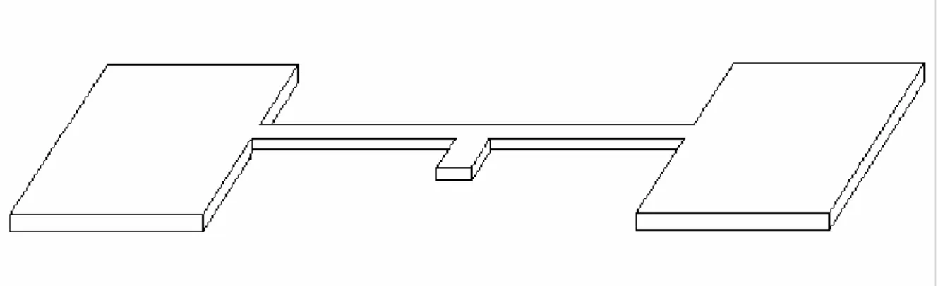
Figure 2.1, Schematic top view of the major fabrication steps of the test TFT’s. Figure 2.2, Current flow lines simulated by MEDICI in
(a) the conventional structure with LBchB = 1 0 µm and WBchB = WBsdB = 5 µm; (b) the test structure with LBchB = 3 µm, WBsdB = 5 µm and WBchB = 30 µm; (c) the test structure with LBchB = 10 µm, WBsdB = 5 µm and WBchB = 30 µm; (d) the test structure with LBchB = 10 µm, WBsdB = 10 µm and WBchB = 30 µm.
Figure 2.3, The equivalent circuit of the channel region of the test structure (RBm,cB is the main channel resistance; RBs,cB is the side channel resistance)
Figure 2.4, (a) IBdsB-VBgsB transfer characteristics; (b) IBdsB-VBdsB output characteristics of the test structure of LBchB / WBsdB = 1 0 µm / 5 µm with different side channel widths (Wsc) compared with the conventional structure.
Figure 2.5, (a) IBdsB-VBgsB transfer characteristics;
(b) IBdsB-VBdsB output characteristics of the test structure of LBchB / WBsdB = 5 µm / 15 µm with different side channel widths (Wsc) compared with the conventional structure.
Figure 2.6, The distributions of the ON-state drain currents of the test structure with (a) Wsd = 1 um ,Vds = 5V; Vgs = 30 V (b) Wsd = 1 um ,Vds = 10V; Vgs = 30 V (c) Wsd = 2 um ,Vds = 5V; Vgs = 30 V (d) Wsd = 2 um ,Vds = 10V; Vgs = 30 V (e) Wsd = 5 um ,Vds = 5V; Vgs = 30 V (f) Wsd = 10 um ,Vds = 5V; Vgs = 30 V
Figure 2.7, The average values of the ON-state drain current gain ABiB of the test structure with (a) Wsd = 1um, Vds = 5 V, Vgs = 30 V
(c) Wsd = 2um, Vds = 5 V, Vgs = 30 V (d) Wsd = 2um, Vds = 10 V, Vgs = 30 V (e) Wsd = 5um, Vds = 5 V, Vgs = 30 V (f) Wsd = 10um, Vds = 5 V, Vgs = 30 V as a function of the side channel width WBscB.
Figure 2.8, The distributions of the ON-state drain current gain ABiB of the test structure with (a) WBscB = 6 µm; (b) WBscB = 1 4 µm against with the channel length LBch Bfor WBsdB = 5 µm and WBsdB = 10µm.
Figure 2.9, The distributions of the ON-state drain current gain ABiB of the test structure with (a) WBscB = 6 µm; (b) WBscB = 1 4 µm against with the channel length to source/drain width ratio LBchB/ WBsdB for WBsdB = 5 µm and WBsdB = 10µm.
Figure 2.10, The experimental and calculated maximum ON-state drain current of the test structure with different source/drain widths and different applied drain biases against with the channel length LBchB, in which the solid symbols represented the experimental data and the empty symbols represented the calculated data obtained from the equation (5).
Figure 2.11, The distributions of the ON-state drain current gain ABiB of the test structure with (a) WBscB = 6 µm
(b) WBscB = 1 4 µm
against with the channel length LBchB for WBsdB = 1 µm and WBsdB = 2µm.
Figure 2.12, The distributions of the ON-state drain current gain ABiB of the test structure with (a) WBscB = 6 µm;
(b) WBscB = 1 4 µm against with the channel length to source/drain width ratio LBchB/ WBsdB for WBsdB=1µm and WBsdB=2µm.
Figure 2.13, The experimental and calculated maximum ON-state drain current of the test structure with different source/drain widths and different applied drain biases against with the channel length LBchB, in which the solid symbols represented the experimental data and the empty symbols represented the calculated data obtained from the equation (7) and equation (9).
Figure 3.1, Schematic top view of the major fabrication steps of the test TFT structure Uwith a half side channel region in the linear region.
Figure 3.2, The distributions of the ON-state drain currents of the test structure Uwith a half side channel region in the linear region.
(a) Wsd = 2 um ,Vds = 5V; Vgs = 30 V (b) Wsd = 2 um ,Vds = 10V; Vgs = 30 V (c) Wsd = 5 um ,Vds = 5V; Vgs = 30 V (d) Wsd = 5 um ,Vds = 10V; Vgs = 30 V
Figure 3.3, The average values of the ON-state drain current gain ABiB of the test structure Uwith a half side channel region in the linear region.
(a) Wsd = 2um, Vds = 5 V, Vgs = 30 V (b) Wsd = 2um, Vds = 10 V, Vgs = 30 V (c) Wsd = 5um, Vds = 5 V, Vgs = 30 V
(c) Wsd = 5um, Vds = 10 V, Vgs = 30 V
Figure 3.4, The distributions of the ON-state drain current gain ABiB of the test structure Uwith a half side channel region in the linear region. UWBscB = 14 µm against with the channel length to source/drain width ratio LBchB/ WBsdB for WBsdB=2µm and WBsdB=5µm.
Figure all
-20 -10 0 10 20 30 10-11 10-10 10-9 10-8 10-7 10-6 10-5 10-4 20 25 30 35 100 200 Wsc = 0 µm 2 µm 4 µm 6 µm 14 µm Dr a in c ur re nt ( µ A) Gate voltage (V) Wsd/Lch = 10/5 µm/µm @ Vds = 5 V Wsc = 0 µm 2 µm 4 µm 6 µm 14 µm D rai n cu rrent ( A ) Gate voltage (V) Figure 2.4(a) 0 5 10 15 20 25 0 100 200 300 400 500 600 700 800 Wsc = 0 µm 2 µm 4 µm 6 µm 10 µm 14 µm Wsd/Lch = 10/5 µm/µm @ Vgs = 30 V Dr ain Curr ent ( µ A) Drain Voltage (V) (Vgs = 30 V; Vds = 5 V ) Figure 2.4(b)
-20 -10 0 10 20 30 10-12 10-11 10-10 10-9 10-8 10-7 10-6 10-5 10-4 20 30 30 60 Wsc = 0 µm 2 µm 4 µm 6 µm 14 µm D rai n c ur rent ( µ A) Gate voltage (V) Wsc = 0 µm 2 µm 4 µm 6 µm 14 µm Wsd/Lch = 5/15 µm/µm @ Vds = 5 V Drain current ( A ) Gate voltage (V) Figure 2.5(a) 0 5 10 15 20 25 0 20 40 60 80 100 120 140 160 180 200 Wsd/Lch = 5/15 µm/µm @ Vgs = 30 V Wsc = 0 µm 2 µm 4 µm 6 µm 10 µm 14 µm Dr ain Curre nt ( µ A) Drain Voltage (V) (Vgs = 30 V; Vds = 5 V ) Figure 2.5(b)
-4 -2 0 2 4 6 8 10 12 14 16 18 20 0 10 20 30 40 50 60 70 80 90 Lch = 3 µm 5 µm 7 µm 10 µm 15 µm Wsd = 1 µm @ Vds = 5 V; Vgs = 30 V Dr a in Cu rr e n t , I ds ( µ A) Wsc=((Wch- Wsd)/2), (µm) Wch = Wsd Figure 2.6(a) -4 -2 0 2 4 6 8 10 12 14 16 18 20 0 20 40 60 80 100 120 140 160 180 Lch = 3 µm 5 µm 7 µm 10 µm 15 µm Wsd = 1 µm @ Vds = 10 V; Vgs = 30 V Dra in Cur re n t , I ds ( µ A) Wsc=((Wch- Wsd)/2), (µm) Figure 2.6(b)
-4 -2 0 2 4 6 8 10 12 14 16 18 20 10 20 30 40 50 60 70 80 90 100 110 120 130 Wsd = 2 µm @ Vds = 5 V; Vgs = 30 V Lch = 3 µm 5 µm 7 µm 10 µm 15 µm Dr ain Cur re nt , I ds ( µ A) Wsc=((Wch- Wsd)/2), (µm) Wch = Wsd Figure 2.6(c) -4 -2 0 2 4 6 8 10 12 14 16 18 20 0 20 40 60 80 100 120 140 160 180 200 220 240 Wsd = 2 µm @ Vds = 10 V; Vgs = 30 V Lch = 3 µm 5 µm 7 µm 10 µm 15 µm Drai n Current , I ds ( µ A) Wsc=((Wch- Wsd)/2), (µm) Wch = Wsd Figure 2.6(d)
-2 0 2 4 6 8 10 12 14 16 18 20 0 20 40 60 80 100 120 140 Lch= 3µm 5µm 7µm 10µm 15µm Drain current , Ids ( µ A ) Wsc=((Wch- Wsd)/2), (µm) Wsd= 5 µm @Vds = 5 V ; Vgs = 30 V Wch = Wsd Figure 2.6(e) -2 0 2 4 6 8 10 12 14 16 18 20 0 40 80 120 160 200 240 280 Wch = Wsd Lch = 3 µm 5 µm 7 µm 10 µm 15 µm Dr ain Curr ent , I ds ( µ A) Wsc=((Wch- Wsd)/2), (µm) Wsd = 10 µm @ Vds = 5 V; Vgs = 30 V Figure 2.6(f)
-2 0 2 4 6 8 10 12 14 16 18 20 0 100 200 300 400 500 600 Lch = 3 µm 5 µm 7 µm 10 µm 15 µm Wsd = 1 µm @ Vds = 5 V; Vgs = 30 V A verage val ue of Ai , ( % ) Wsc=((Wch- Wsd)/2), (µm) Figure 2.7(a) -2 0 2 4 6 8 10 12 14 16 18 20 0 100 200 300 400 500 600 Lch = 3 µm 5 µm 7 µm 10 µm 15 µm Wsd = 1 µm @ Vds = 10 V; Vgs = 30 V Aver age val u e of Ai , (% ) Wsc=((Wch- Wsd)/2), (µm) Figure 2.7(b)
-2 0 2 4 6 8 10 12 14 16 18 20 0 100 200 300 400 Lch = 3 µm 5 µm 7 µm 10 µm 15 µm Wsd = 2 µm @ Vds = 5 V; Vgs = 30 V Aver age value of A i, ( % ) Wsc=((Wch- Wsd)/2), (µm) Figure 2.7(c) -2 0 2 4 6 8 10 12 14 16 18 20 0 100 200 300 400 Lch = 3 µm 5 µm 7 µm 10 µm 15 µm Wsd = 2 µm @ Vds = 10 V; Vgs = 30 V A verage val u e of A i, (%) Wsc=((Wch- Wsd)/2), (µm) Figure 2.7(d)
-2 0 2 4 6 8 10 12 14 16 18 20 0 20 40 60 80 100 120 140 Wsd= 5 µm @Vds = 5 V ; Vgs = 30 V Lch= 3 µm 5 µm 7 µm 10 µm 15 µm ∆Wch=( (Wch- Wsd)/2), (µm) Average val ue of A i ,(%) "Saturation" Point Figure 2.7(e) -2 0 2 4 6 8 10 12 14 16 18 20 0 10 20 30 40 50 60 70 80 90 "Saturation" Point Wsd = 10 µm @ Vds = 5 V; Vgs = 30 V Average value of A i ,(%) Wsc=((Wch- Wsd)/2), (µm) Lch = 3 µm 5 µm 7 µm 10 µm 15 µm Figure 2.7(f)
0 2 4 6 8 10 12 14 16 18 20 0 10 20 30 40 50 60 70 80 90 100 110 120 130 divergence point @Vds = 5 V; Vgs = 30 V Wsc = 6 µm Wsd = 5 µm Wsd = 10 µm Ai = ( I ds,t - I ds, c ) /Ids, c , (%) Lch divergence point intercept~1.55 Figure 2.8(a) 0 2 4 6 8 10 12 14 16 18 20 0 10 20 30 40 50 60 70 80 90 100 110 120 130 divergence point @Vds = 5 V; Vgs = 30 V Wsc = 14 µm Wsd = 5 µm Wsd = 10 µm Ai = (Ids,t - I ds,c )/Ids,c , (%) Lch intercept~1.55 Figure 2.8(b)
0.0 0.5 1.0 1.5 2.0 2.5 3.0 0 10 20 30 40 50 60 70 80 90 100 110 120 130 slope~0.48 divergence point divergence point @Vds = 5 V; Vgs = 30 V Wsc = 6 µm Wsd = 5 µm Wsd = 10 µm A i = ( I ds,t - I ds, c ) /I ds ,c , (%) Lch/Wsd slope~0.48 Figure 2.9(a) 0.0 0.5 1.0 1.5 2.0 2.5 3.0 0 10 20 30 40 50 60 70 80 90 100 110 120 130 divergence point Wsd = 5 µm Wsd = 10 µm @Vds = 5 V; Vgs = 30 V Wsc = 14 µm Ai = (I ds,t - Ids ,c )/Ids, c , (%) Lch/Wsd slope~0.48 slope~0.47 Figure 2.9(b)
0 2 4 6 8 10 12 14 16 18 50 100 150 200 250 300 350 400 450 Wsd= 10 µm; Vds= 5 V Experimental data Calculated data Ma ximum Dra in Cur re nt ( µ A) Lch @ Vgs =30 V Wsd= 10 µm; Vds= 10 V (Wsd= 5 µm; Vds= 10 V) Wsd= 5 µm; Vds= 5 V Figure 2.10
-2 0 2 4 6 8 10 12 14 16 18 20 50 100 150 200 250 300 350 400 450 500 intercept ~ 0.61 @Vds = 5 V; Vgs = 30 V Wsc = 6 µm Wsd = 1 µm Wsd = 2 µm Ai = ( I ds, t - Ids ,c ) /Ids,c , (%) Lch Figure 2.11(a) -2 0 2 4 6 8 10 12 14 16 18 20 0 100 200 300 400 500 @Vds = 5 V; Vgs = 30 V Wsc = 14 µm Wsd = 1 µm Wsd = 2 µm A i = ( I ds,t - I ds, c )/ I ds,c , (%) Lch intercept ~ 0.0 Figure 2.11(b)
-2 0 2 4 6 8 10 12 14 16 18 50 100 150 200 250 300 350 400 450 500 @Vds = 5 V; Vgs = 30 V Wsc = 6 µm Wsd = 1 µm Wsd = 2 µm A i = ( I ds,t - I ds,c ) /I ds,c , ( % ) Lch/Wsd slope ~0.32 slope~0.36 Figure 2.12(a) -2 0 2 4 6 8 10 12 14 16 0 100 200 300 400 500 slope ~0.34 slope ~0.42 @Vds = 5 V; Vgs = 30 V Wsc = 14 µm Wsd = 1 µm Wsd = 2 µm A i = ( I ds,t - I ds,c )/I ds, c , (%) Lch/Wsd Figure 2.12(b)
0 2 4 6 8 10 12 14 16 18 20 20 40 60 80 100 120 140 160 180 200 220 Wsd= 1 µm; Vds= 5 V Wsd= 2 µm; Vds= 5 V Wsd= 1 µm; Vds= 10 V Wsd= 2 µm; Vds= 10 V @ Vgs =30 V
Experimental data
Calculated data
Saturated Dr
ain Current (
µA)
Lch
Figure 2.13-4 -2 0 2 4 6 8 10 12 14 16 18 20 0 10 20 30 40 50 60 70 80 90 100 110 120 Wsd = 2 µm @ Vds = 5 V; Vgs = 30 V
Half Side Channel
Lch = 3 µm 5 µm 7 µm 10 µm 15 µm Drain Current , I ds ( µ A) Wsc=(Wch- Wsd), (µm) Wch = Wsd Figure 3.2(a) -4 -2 0 2 4 6 8 10 12 14 16 18 20 0 20 40 60 80 100 120 140 160 180 200 220 240 Wsd = 2 µm @ Vds = 10 V; Vgs = 30 V
Half side Channel
Lch = 3 µm 5 µm 7 µm 10 µm 15 µm Drain Curre nt , I ds ( µ A) Wsc=(Wch- Wsd), (µm) Wch = Wsd Figure 3.2(b)
-4 -2 0 2 4 6 8 10 12 14 16 18 20 0 20 40 60 80 100 120 140 160 180 200 220 240 Wsd = 5 µm @ Vds = 5 V; Vgs = 30 V
Half Side Channel
Lch = 3 µm 5 µm 7 µm 10 µm 15 µm Drain Current , I ds ( µ A) Wsc=(Wch- Wsd), (µm) Wch = Wsd Figure 3.2(c) -4 -2 0 2 4 6 8 10 12 14 16 18 20 0 40 80 120 160 200 240 280 320 360 400 440 480 Wsd = 5 µm @ Vds = 10 V; Vgs = 30 V
Half Side Channel
Lch = 3 µm 5 µm 7 µm 10 µm 15 µm Drain Cur rent , I ds ( µ A) Wsc=(Wch- Wsd), (µm) Wch = Wsd Figure 3.2(d)
-2 0 2 4 6 8 10 12 14 16 18 20 0 50 100 150 200 Lch = 3 µm 5 µm 7 µm 10 µm 15 µm Wsd = 2 µm @ Vds = 5 V; Vgs = 30 V Half Side-Channel Aver age val ue of A i, (%) Wsc=(Wch- Wsd), (µm) Figure 3.3(a) -2 0 2 4 6 8 10 12 14 16 18 20 0 50 100 150 200 Lch = 3 µm 5 µm 7 µm 10 µm 15 µm Wsd = 2 µm @ Vds = 10 V; Vgs = 30 V Half Side-Channel Aver age va lu e of A i, ( % ) Wsc=(Wch- Wsd), (µm) Figure 3.3(b)
-2 0 2 4 6 8 10 12 14 16 18 20 0 20 40 60 80 100 Lch = 3 µm 5 µm 7 µm 10 µm 15 µm Wsd = 5 µm @ Vds = 5 V; Vgs = 30 V Half Side-Channel Av er age value of A i, (%) Wsc=(Wch- Wsd), (µm) Figure 3.3(c) -2 0 2 4 6 8 10 12 14 16 18 20 0 20 40 60 80 100 Lch = 3 µm 5 µm 7 µm 10 µm 15 µm Wsd = 5 µm @ Vds = 10 V; Vgs = 30 V Half Side-Channel
Averag
e val
u
e o
f A
i, (%)
Wsc=(Wch- Wsd), (
µm)
Figure 3.3(d)-2 0 2 4 6 8 10 20 40 60 80 100 120 140 160 180 slope ~ 0.24 @Vds = 5 V; Vgs = 30 V Wsc = 14 µm Half Side-Channel Wsd = 5 µm Wsd = 2 µm Ai = (Ids ,t - I ds, c )/Ids ,c , ( % ) Lch/Wsd slope ~ 0.30 Figure 3.4