國 立 交 通 大 學
電子工程學系
電子研究所碩士班
碩 士 論 文
利用化學機械研磨技術製作新穎多晶矽薄膜電晶體結構及
其電性模擬
The Fabrications and Simulations of a Novel Poly-Si TFT
Structure Using CMP Technology
學生:楊國良
Student:
Guo-Liang Yang
指導教授:張國明 博士 Advisor:
Dr. Kow-Ming Chang
桂正楣 博士 Dr. Cheng-May Kwei
利用化學機械研磨技術製作新穎多晶矽薄膜電晶體結構及其電性
模擬
The Fabrications and Simulations of a Novel Poly-Si TFT
Structure Using CMP Technology
研 究 生:楊國良 Student:Guo-Liang Yang
指導教授:張國明 博士 Advisor:Dr. Kow-Ming Chang
桂正楣 博士 Dr. Cheng-May Kwei
國 立 交 通 大 學
電 子 工 程 學 系 電 子 研 究 所 碩 士 班
碩 士 論 文
A Thesis
Submitted to Department of Electronics Engineering & Institute of Electronics College of Electrical and Computer Engineering
National Chiao Tung University in Partial Fulfillment of the Requirements
for the Degree of Master of Science
in
Electronics Engineering July 2006
Hsinchu, Taiwan, Republic of China
利用化學機械研磨技術製作新穎多晶矽薄膜電晶體結構及
其電性模擬
研究生:楊國良 指導教授:張國明 博士
桂正楣 博士
國立交通大學
電子工程學系 電子研究所碩士班
摘要
本篇論文中,我們將探討和比較利用化學機械研磨技術所製作的新穎結構,此新 穎結構具有加厚的汲/源極和一個薄通道。從模擬的結果來看,因為較厚的源/汲極,在 較厚的通道內的側向電場能被降低,所以漏電流可能會降低。而且成功的使漏電流下降 了一個數量級。我們提供了一個使用化學機械研磨技術的新穎堆疊結構取代傳統的堆疊 式結構,而且此製程能完全的與傳統四道製程相容。The Fabrications and Simulations of a Novel Poly-Si TFT
Structure Using CMP Technology
Student: Guo-Liang Yang Advisor: Dr. Kow-Ming Chang Dr. Cheng-May Kwei
Department of Electronic Engineering & Institute of Electronics National Chiao Tung University
Abstract
In this thesis, the characteristics of the novel structure of poly-Si TFTs with thick S/D and thin channel by using CMP process have been investigated and compared. From the simulated results, the lateral electric field in the thicker channel near the drain region can be reduced with the thick S/D region, so the off-state current could be decreased. Moreover, we have succeeded to reduce the off-state current at least 1 orders. We proposed the novel staggered structure with CMP technology instead of conventional staggered structure, and the fabrication processes are fully compatible with the conventional four-mask ones. This structure may be an attractive device structure for future high-perform large-area device application.
誌謝
能完成這篇論文,要感謝很多人,首先要先感謝我的父母,在背後默默的支持與關 心,讓我在研究生的兩年,能夠安心的完成我的學業。 感謝我的指導教授張國明教授與桂正楣教授,老師開明的態度跟指導教誨讓我的研 究生涯受益良多,在每次的聚會或是書報時,老師都會信心喊話,提升大家的士氣,就 像生活在一個大家庭一樣。 感謝林俊銘學長在實驗方面給我相當多的幫助,在發生問題時也提供了相當寶貴的 意見,還有感謝同屆的好同學,在這忙碌的實驗過程中互相幫忙及分享各種實驗技巧, 也感謝所有認識的學長對我的指導與照顧。也感謝學弟妹們陪我打球解解悶。最後也謝 謝交大奈米中心及 NDL 提供了完整的機台讓我順利的完成我的研究。 兩年的研究生活,說長不長,說短也不短。在這兩年裡,發生了很多事,有喜悅, 有悲傷,也經歷了人生的大起大落。多虧了大家的幫忙,才能順利的完成我的論文,謝 謝你們!!Contents
Chinese Abstract ……….………..………...i
English Abstract ……….……….ii
Acknowledgements ………....………iii
Contents ……….…....iv
Table Captions ………...vi
Figure Captions ………...……….……….vii
Chapter 1 Introduction ………..………....…1
1.1 Overview of Low Temperature Polycrystalline Silicon (LTPS) Thin-film Transistors (TFTs) 1.2 Issues in LTPS TFTs 1.3 Motivations 1.4 Thesis Organization Chapter 2 Simulations of the Novel LTPS TFT’s structures ……….4
2.1 The Structures of Novel LTPS TFT’s 2.2 The Results of Simulations 2.3 Summary Chapter 3 Experimental of the Novel Structure LTPS TFTs ………...…..7
3.1 The Fabrication Process Flow of Low Temperature Poly-Si TFTs 3.2 Methods of Device Parameter Extraction 3.2.1 Determination of Threshold Voltage (Vth) 3.2.2 Determination of the On/off Current ratio Chapter 4 The Characteristics of the Novel Damascene-gated Low-temperature Poly-Si TFTs with Staggered Source/Drain Regions ………...…....11
4.1 The Characteristics of the Novel Damascene-gated Low-temperature Poly-Si TFTs with Staggered Source/Drain compared with the Conventional TFTs 4.2 Comparisons of the Leakage Current in Off-State Operation and the On/Off Current Ratio 4.3 The Output Characteristics of the Proposed Structures Compared with the Conventional Structure 4.4 Comparison of the Proposed Structure and the Conventional Staggered Structure with Five Masks Chapter 5 Conclusions and future work ...………...………...14
5.2 Future work
Table captions
Table I. The simulated maximum lateral electric field near the drain region of the conventional and the damascene-gated TFTs at the three sampling points. The maximum was simulated at VGS = 0 V and VDS = 20 V
Table II. The simulated maximum lateral electric field near the drain region of the conventional and the damascene-gated TFTs at the three sampling points. The maximum was simulated at VGS = 30 V and VDS = 20 V
Table III. The characteristics of the drain current in IDS – VGS plot of the conventional and
Figure captions
Chapter 1
Fig. 1-1(a) The top-gate coplanar TFT Fig. 1-1(b) The bottom-gate TFT
Fig. 1-2 The basic structure of an n-channel poly-Si TFT and its band diagram with the
three kinds of leakage current mechanisms. G: The generation current, T1: the thermionic field emission current, T2: the field emission current, Efns: quasi-Fermi
level of electron at the source, Efp : quasi-Fermi level of hole, Efnd : quasi-Fermi
level of electron at the drain
Chapter 2
Fig. 2-1 The simulated proposed structure
Fig. 2-2 The sampling positions of the damascene-gated and conventional structures
Fig. 2-3(a) The simulated lateral electric field of the conventional structure in off-sate operation
Fig. 2-3(b) The simulated lateral electric field of the 300 nm damascene-gated structure in off-sate operation
Fig. 2-3(c) The simulated lateral electric field of the 100 nm damascene-gated structure in off-sate operation
Fig. 2-3(d) The simulated lateral electric field of the 200 nm damascene-gated structure in off-sate operation
Fig. 2-4(a) The simulated potential distribution of the conventional structure in off-sate operation
Fig. 2-4(b) The simulated potential distribution of the 100 nm damascene-gated structure in off-sate operation
Fig. 2-4(c) The simulated potential distribution of the 200 nm damascene-gated structure in off-sate operation
Fig. 2-4(d) The simulated potential distribution of the 300 nm damascene-gated structure in off-sate operation
Fig. 2-5(a) The simulated current flow of the conventional structure in off-sate operation Fig. 2-5(b) The simulated current flow of the 100 nm damascene-gated structure in off-sate
operation
Fig. 2-5(c) The simulated current flow of the 200 nm damascene-gated structure in off-sate operation
Fig. 2-5(d) The simulated current flow of the 300 nm damascene-gated structure in off-sate operation
Fig. 2-6(a) The simulated lateral electric field of the conventional structure in on-sate operation
Fig. 2-6(b) The simulated lateral electric field of the 300 nm damascene-gated structure in on-sate operation
Fig. 2-6(c) The simulated lateral electric field of the 100 nm damascene-gated structure in on-sate operation
Fig. 2-6(d) The simulated lateral electric field of the 200 nm damascene-gated structure in on-sate operation
Fig. 2-7(a) The simulated potential distribution of the conventional structure in on-sate operation
Fig. 2-7(b) The simulated potential distribution of the 100 nm damascene-gated structure in on-sate operation
Fig. 2-7(c) The simulated potential distribution of the 200 nm damascene-gated structure in on-sate operation
Fig. 2-7(d) The simulated potential distribution of the 300 nm damascene-gated structure in on-sate operation
Chapter 3
Fig. 3-1 Process flow of fabricating low-temperature damascene-gated TFTs with thick S/D
and thin channel
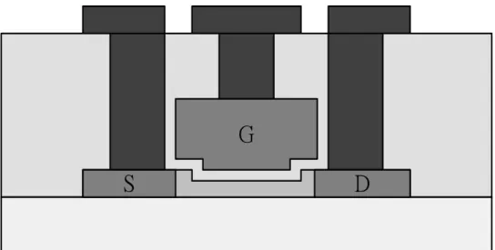
Fig. 3-2 The conventional TFT
Chapter 4
Fig. 4-1 IDS – VGS transfer characteristics of the proposed structure and conventional
structure TFTs for VDS = 5 V; W/L = 5 µm/5 µm
Fig. 4-2 IDS – VGS transfer characteristics of the proposed structure and conventional
structure TFTs for VDS = 10 V; W/L = 5 µm/5 µm
Fig. 4-3 IDS – VGS transfer characteristics of the proposed structure and conventional
structure TFTs for VDS = 5 V; W/L = 10 µm/5 µm
Fig. 4-4 IDS – VGS transfer characteristics of the proposed structure and conventional
structure TFTs for VDS = 10 V; W/L = 10 µm/5 µm
Fig. 4-5 IDS – VGS transfer characteristics of the proposed structure and conventional
structure TFTs for VDS = 5 V; W/L = 5 µm/15 µm
Fig. 4-6 IDS – VGS transfer characteristics of the proposed structure and conventional
Fig. 4-7 IDS – VGS transfer characteristics of the proposed structure and conventional
structure TFTs for VDS = 5 V; W/L = 10 µm/15 µm
Fig. 4-8 IDS – VGS transfer characteristics of the proposed structure and conventional
structure TFTs for VDS = 10 V; W/L = 10 µm/15 µm
Fig. 4-9 IDS – VDS output characteristics of the proposed structure and conventional
structure TFTs; W/L = 5 µm/5 µm
Fig. 4-10 IDS – VDS output characteristics of the proposed structure and conventional
structure TFTs; W/L = 10 µm/5 µm
Fig. 4-11 IDS – VDS output characteristics of the proposed structure and conventional
structure TFTs; W/L = 5 µm/15 µm
Fig. 4-12 IDS – VDS output characteristics of the proposed structure and conventional
structure TFTs; W/L = 10 µm/15 µm
Fig. 4-13 IDS – VGS transfer characteristics of the proposed structure and conventional
Chapter 1
Introduction
1.1 Overview of Low Temperature Polycrystalline Silicon (LTPS)
Thin-film Transistors (TFTs)
Polycrystalline Silicon (poly-Si) thin-film transistors (TFTs) fabricated at low temperature have attracted attention for high-density SRAMs [1][2], linear image sensors [3], photodetector amplifier [4], and nonvolatile memories [5] etc, especially peripheral driving circuits in AMLCDs [6]-[9].
Recrystallization technology is important for low temperature Poly-Si TFTs because of the grain size, grain boundary and intragranular defects [10], which influence the performance of Poly-Si TFTs. To achieve the bigger grain size, better performance and low temperature process, we have some useful recrystallization technologies: solid phase crystallization (SPC) [11], eximer laser annealing (ELA) [12]-[14], and metal-induced lateral crystallization (MILC) [15]-[17] etc. In this paper, we used SPC method to recrystallize the poly-Si TFTs.
In generally, poly-Si TFTs have two structures: top-gate coplanar structure and bottom-gate structure as shown in Figure 1-1. The top-gate TFTs are mainly used in AMLCD application because their self-aligned source/drain regions provide low parasitic capacitances and are suitable for device scaling down. On the other hand, Bottom-gate TFTs have better interface and higher plasma hydrogenation rate than top-gate TFTs, but they have lower current and need extra process steps for backside exposure and difficult fabrication.
The dominant leakage current mechanism in poly-Si TFTs is the field emission via the grain boundary traps by a high electric field near the drain [18]. Therefore, reducing the
lateral electric field near the drain junction is needed. For example, using a lightly doping drain (LDD) structure can reduced the lateral electric field [19][20]. The LDD structure certainly not only reduces the electric field but also enhances source/drain series resistance that limits the on-state current.
Besides LDD structure, many device structures are used to enhance poly-Si TFTs performance, such as offset gate [21][22], gate-overlapped LDD [23]-[25], multi-channel structure [26].
1.2 Issues in LTPS TFTs
Although we usually use the poly-Si TFTs instead of the amorphous TFTs for the high mobility, the poly-Si TFTs suffer from the high leakage current in the off-state operation and kink effect in the on-state operation. Besides, under the long-term operation, the stability of the poly-Si TFTs is a major issue. The hot carrier effect is also an important reliability in LTPS TFTs.
It is well known that there are three kinds of the leakage current mechanisms in poly-Si
TFTs [27]. First, when the drain voltage is very low, the leakage current is governed by
thermally generated carriers via trap states, which is denoted by G in Figure 1-2. Second, when the drain voltage is in the intermediate range, the leakage current is generated by the thermionic field emission of electrons indicated as T1 in Figure 1-2. In this case the electrons in the valence band are thermally excited to the trap states, and then tunnel to the conduction band quantum mechanically. The leakage current therefore increases with the gate voltage due to the narrowing of the barrier width. Third, when the gate voltage is high enough, the leakage current is governed by the field enhanced tunneling which is denoted by T2 and T1 in Figure 1-2. Obviously, decreasing the drain electric field is helpful to reducing the leakage current.
1.3 Motivations
The high off-state leakage current and the on-state kink effect are the influences on the properties of poly-Si TFTs, which even have higher on-state current than the amorphous Si TFTs. In this study, we used the Damascene process to form the thin channel with partially thicker region structure, which not only effectively reduces the drain electric field but also shows a low leakage current [28][29]. Besides, we also combine thick S/D and thin channel to achieve the purposes of low off-state current and drain electric field. In this process, an additional mask will not be required.
1.4 Thesis Organization
In chapter 1, a brief overview of LTPS TFT technology and related applications were introduced.
In chapter 2, the simulations of the novel LTPS TFTs, including the lateral electric field, the potential distribution, and the current flow, will be described.
In chapter 3, the fabrication process flow of the novel LTPS TFT device and experimental recipes will be presented.
In chapter 4, we will show the electrical properties of the novel poly-Si TFT device, which contain transfer characterization and output characterization
Finally, conclusions and future work as well as suggestion for further research are given in chapter 5.
Chapter 2
Simulations of the Novel LTPS TFT’s Structures
2.1 The Structures of Novel LTPS TFT’s
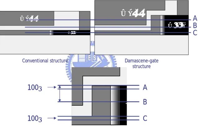
In this thesis, we provide a new architecture, which combines thicker source/drain, thin channel and damascene-gate structure, and use MEDICI to simulate the structure. Figure 2-1 shows the structure of the proposed poly-Si TFTs. The thickness of the channel is 500 Å. Gate oxide thickness is also 500 Å. The thick source/drain has different thickness with 1000 Å, 2000 Å, and 3000 Å, respectively. The partial thicker channel thickness is the same as the source/darin. We also simulated the conventional coplanar structure with 500 Å channel layer.
2.2 The Results of Simulations
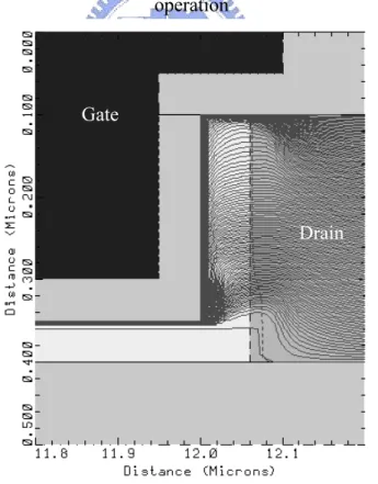
We primarily simulated the electric field in the on-state and off-state operation and the effects of electric fields to the current flow distribution. The sampling positions are shown in Figure 2-2. The line A is located below the thick source/drain surface 100 Å. The line B lies to the middle position between the surface of thick source/drain and the channel surface. The line C is under the channel surface 100 Å.
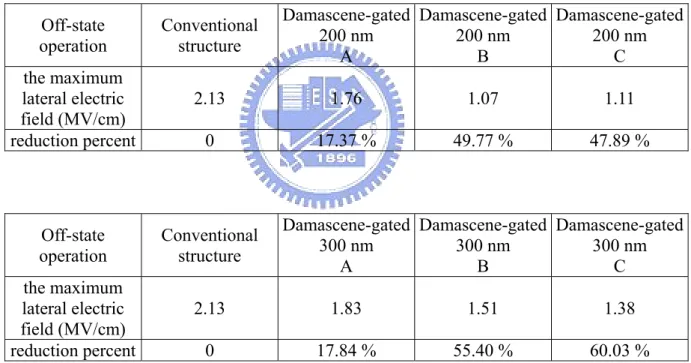
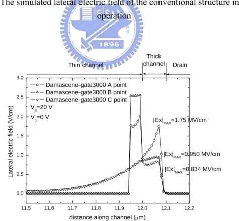
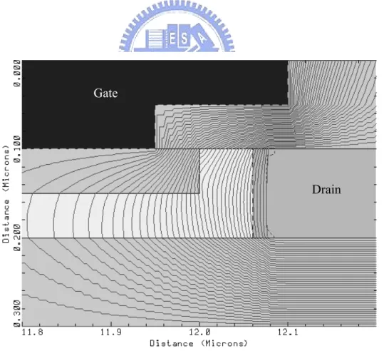
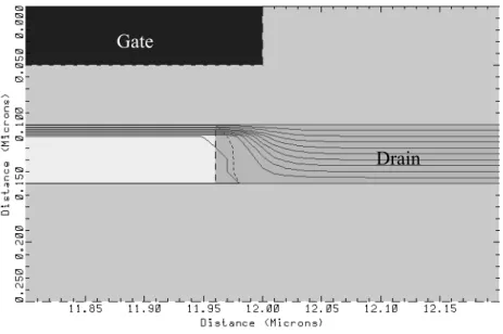
Figure 2-3 shows the simulated the lateral electric fields of a conventional TFT and the proposed TFTs in the off-state operation. Obviously, the electric field of the proposed TFT is lower than which of a conventional TFT. Figure 2-4 shows the potential distributions of the proposed TFTs and a conventional TFT to confirm the electric field. The results predict that
the leakage current can be reduced by lowering the lateral electric field near the drain region. For example of the damascene-gated structure with 3000 Å Source/Drain, the reduction percent of the maximum lateral electric fields near the drain region are 17.84 %, 55.40 %, and 60.03 % at three sampling points, respectively, compared with the conventional ones. Moreover, the maximum lateral electric field near the drain region is reduced with increasing the source/drain thickness of the damascene-gated structure. The values and reduction percent of the maximum lateral electric fields near the drain region in off-state operation are shown in the Table I.
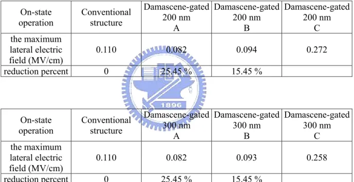
On the other hand, in the on-state operation, Figure 2-5 shows the simulated current flow. Obviously, the main current path is near the channel surface. It means that the primary influence on the on-state current is the surface lateral electric field near the drain region. The on-state electric field is shown in the Figure 2-6. Although the maximum lateral electric fields at the line B and C of proposed structure are higher than which of conventional structure, the on-state current is not affected remarkably. The lower lateral electric field at line A may result the on-state current reducing slightly, and it is expected to suppress the kink effect. Table II show the values and reduction percent of the maximum lateral electric fields near the drain region in on-state operation
In Figure 2-3 and 2-6, it is noted that larger the electric fields of proposed TFT from 11.5 nm to 12 nm along the channel direction result from the sampling line crossing the oxide layer.
2.3 Summary
It clearly shows that the lateral electric field near the drain region of the proposed TFT is lower than which of the conventional TFT. The simulated results show that the lateral electric
field near the drain region can be effectively reduced by the proposed structure, and it can be expected that the better performance of the proposed structures would be obtained.
Chapter 3
Experimental of the Novel Structure LTPS TFTs
3.1 The Fabrication Process Flow of Low Temperature Poly-Si TFTs
The poly-Si TFTs were fabricated on 6-inch-diameter p-type silicon wafer. Figure 3-1 shows the process flow of the proposed poly-Si TFTs. The undoped amorphous silicon (α-Si) film was initially deposited on 500 nm thermally oxide silicon (100) wafers by low
temperature chemical vapor deposition (LPCVD) system with silane (SiH4) gas at 620 ℃.
The deposition pressure was 160 mtorr. Then the solid phase crystallization (SPC) process was carried out with 600 ℃, 24 hours. A 400 nm TEOS oxide film was deposited at 300 ℃ as passivation layer by PECVD. Then, the chemical-mechanical polishing (CMP) process was used to flat the surface of TEOS oxide. Gate regions were patterned by reactive ion etching and wet etching. The 50 nm-thick TEOS gate oxide was deposited by PECVD at 300 ℃, sequentially the 400 nm poly-Si film was formed by LPCVD at 620 ℃. Afterwards, CMP process polished the additional poly-Si to form the damascene gate. The passivation oxide layer was removed by the wet etching. Then the region of source, drain and gate were doped
by a self-aligned phosphorus implantation. The dopants were activated at 600 ℃ in N2
ambient for 24 hours. Next, a 300 nm TEOS oxide for a passivation layer was deposited by PECVD at 300 ℃, and the contact lithography was carried out. After opening the contact holes, a 500 nm Al was deposited by the thermal coater and the metal pad was patterned.
Finally, the samples were sintered at 400 ℃ for 30 minutes in N2 ambient. The main
processes of fabrication are shown in Figure 3-1.
same run.
The detail fabrication process flows are listed as follows.
1. (100) orientation Si wafer 2. Initial clean
3. Thermal wet oxidation at 980 ℃ to grow 500 nm thermal SiO2 in furnace
4. α-Si (100 nm, 200 nm and 300 nm) film was deposited by LPCVD at 620 ℃ in SiH4
gas
5. SPC was carried out with 600 ℃ for 24 hrs 6. Mask#1: define S/D
7. Poly-Si film was dry etched by poly-etcher system
8. 400 nm TEOS oxide was deposited by PECVD at 300 ℃ 9. Flatting the surface by CMP process
10. Post clean
11. Mask#2: define gate
12. Oxide and poly-Si film were dry etched, poly-Si need to leave 50 nm as channel 13. Oxide was wet lateral etched
14. RCA clean
15. 50 nm TEOS gate dielectric deposition by PECVD at 300 ℃
16. 400 nm poly-Si gate was deposited by LPCVD at 620 ℃ in SiH4 gas
17. CMP process to remove the additional poly-Si 18. Post clean
19. Passivation oxide layer were removed by wet etching
20. Ion implantation: P31, 5×1015 cm-2, 50 KeV (100 nm), 70 KeV (200 nm) ,100 KeV (300
nm)
22. Initial clean
23. 300 nm TEOS oxide film was deposited by PECVD at 300 ℃ for the passivation layer 24. Mask#3: open contact holes
25. Wet etching by B.O.E
26. 500 nm Al thermal evaporation 27. Mask#4: Al pads definition 28. Etching Al
29. Al sintering at 400 ℃ in N2 ambient for 30 min
3.2 Methods of Device Parameter Extraction
Many methods have been proposed to extract the characteristic parameters of poly-Si TFT. In this section, the methods of parameter extraction used in this research are described.
3.2.1 Determination of Threshold Voltage (Vth)
The threshold voltage Vth is an important MOSFET parameter required for the channel
length-width and series resistance measurement. However, Vth is a voltage that is not uniquely
defined. Various definitions exist and the reason for this can be found in the ID - VGS curve.
One of the most common threshold voltage measurement techniques is the VGS of drain
current of (W/L) × 10-7 A at VD = 5 V.
On/off current ratio is one of the most important parameters of poly-Si TFTs. The leakage current mechanism in poly-Si TFTs is different from MOSFET. In MOSFET, the channel is composed of single-crystalline silicon and the leakage current is due to the tunneling of minority carrier from drain region to accumulation layer located in channel layer region. However, in poly-Si TFTs, the channel is composed of polycrystalline silicon. A large amount of trap densities in grain boundary attribute a lot of defect states in energy band gap to enhance the tunneling effect. Therefore, the leakage current due to the tunneling effect is much larger in poly-Si TFTs than in single-crystalline devices. When the voltage drops increase, the band gap width decrease and the tunneling effect becomes worse. Normally, we can observe this effect in typical poly-Si TFT ID-VG characteristics where the magnitude of
leakage current will reach a minimum and then increase as the gate voltage decrease/increase for n/p-channel TFTs.
There are a lot of ways to specify the on and off current. In this thesis, the on current is defined as the drain current when gate voltage equal to 30 V and drain voltage is 5 V. The off current is specified as the minimum leakage current in linear operation mode for usual cases.
V 5 V at plot V I of current Minimum V 5 V at plot V I of current Maximum I I ratio current off / on DS GS DS DS GS DS min on = − = − = = (Eq. 3.1)
Chapter 4
The Characteristics of the Novel Damascene-gated
Low-temperature Poly-Si TFTs with Staggered
Source/Drain Regions
In this chapter, we will discuss the device performances of our novel structure of the poly-Si TFTs, and also compare with the conventional TFTs. We measured the thickness of the films by n&k analyzer, and the I-V characteristics of poly-Si TFTs by HP4156 semiconductor parameter analyzer.
4.1 The Characteristics of the Novel Damascene-gated Low-temperature
Poly-Si TFTs with Staggered Source/Drain compared with the
Conventional TFTs
Figure 4-1 ~ Figure 4-8 show the IDS – VGS transfer characteristics of the proposed
structure compared with conventional structure. In the negative gate voltage, the leakage current of the proposed structures are lower than which of the conventional structure. In the chapter 2, we have simulated that the lateral electric field near the drain region of the proposed structure is lower than that of the conventional structure, which can suppress the leakage current. On the other hand, the proposed structures have a slightly lower on-state current because of the lower lateral electric field in on-state operation, but the on/off current ratio is affected lightly.
Figure 4-9 ~ Figure 4-12 show the measured IDS – VDS output characteristics of the
proposed TFTs and the conventional ones. In the theory, the lower lateral electric field near the drain region is considered that can suppress the kink effect. However, the kink effect is not suppressed obviously at high driving voltage. It is considered that there are too many grain boundary traps with the increase of the thickness of the S/D region, and the reduction of the lateral electric field near the drain region is limited.
4.2 Comparisons of the Leakage Current in Off-State Operation and the
On/Off Current Ratio
The leakage current in off-state (Ileak) is defined as the drain current (IDS) at the negative
voltage (VGS = -15 V). For the proposed structure with W/L = 10 µm/5 µm in Figure 4-3, the
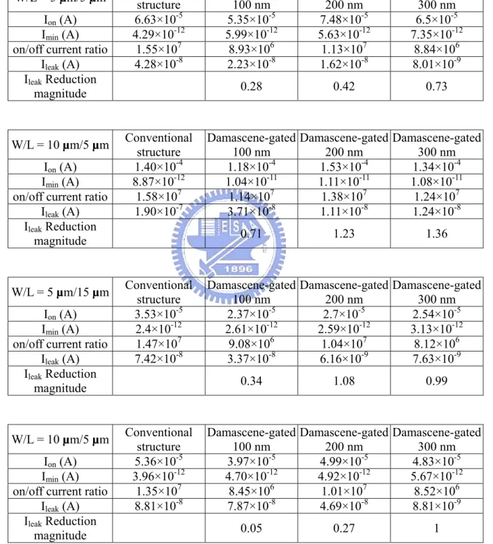
leakage current (Ileak) of the proposed structures with 100-nm, 200-nm, 300-nm source/drain
thickness decreased 0.71, 1.23 and 1.36 order of magnitude, respectively. In the other sizes, the leakage currents of the proposed structure with 300-nm source/drain thickness are all decreased over one order of magnitude at least.
On the other hand, the minimum leakage current (Imin) of the proposed structures are
slightly increased than that of the conventional structure. This is because the proposed structure has more grain boundary traps in the channel near the thicker source/drain region. The on/off current ratio of the conventional structure, and the proposed structures of W/L = 10
µm/5 µm with 100-nm, 200-nm, 300-nm source/drain thickness are 1.58×10⁷, 1.14×10⁷, 1.38×
107, and 1.24×10⁷, respectively. Table III lists the on-state currents (I
on), the minimum leakage
current (Imin), on/off current ratio (Ion/Imin), and off-state currents (Ileak) of the conventional and
4.3 The Output Characteristics of the Proposed Structures Compared with
the Conventional Structure
As shown in Figure 4-9 ~ Figure 4-12, the kink effect of the proposed structures is considered to be suppressed due to the lower electric field near the drain region. At the low driving voltage (|VGS - Vth| = 10 V), the kink current of the proposed structure is much smaller
than that of the conventional structure with W/L = 10 µm/5 µm and W/L = 5 µm/5 µm. As the driving voltage increasing, the kink effect becomes more significant. Although the lateral electric field near the drain region is decreased, it maybe due to large amount of grain boundary traps exists in the thicker channel near the source/drain region.
4.4 Comparison of the Proposed Structure and the Conventional Staggered
Structure with Five Masks
Figure 4-13 shows the transfer characteristics of the proposed TFT and the conventional TFT with staggered source and drain region. It clearly presents that the curve of the proposed structure is almost the same with that of the conventional structure with staggered source and drain region (five masks). Therefore, we proposed a new fabrication with CMP process technology instead of an additional lithography step, and more simple than the conventional five-mask steps staggered source/drain structure.
Chapter 5
Conclusions and future work
5.1 Conclusions
In this thesis, a novel low-temperature poly-Si TFT with a thicker source/drain region and thin channel by using CMP process was proposed and investigated. Although, in our proposed structure, more grain boundary traps existed in the thicker channel region and lower lateral electric field would cause the on/off current ratio slightly decreasing, lower lateral electric field would substantially reduce the leakage current in off-state operation. Moreover, the fabrication processes of the proposed structure are simple and no additional mask step is needed. We proposed the novel staggered structure with CMP technology instead of conventional staggered structure, and the fabrication processes are fully compatible with the conventional four-mask ones. This structure may be an attractive device structure for future high-perform large-area device application.
5.2 Future work
We have proposed a damascene-gated low-temperature poly-Si TFTs with a thicker source/drain region and thin channel to improve the conventional low-temperature poly-Si TFTs performance. However, in order to further improve device electrical characteristics and apply to glass substrates, there will be still some works worth of being investigated.
suppressed due to large number of the grain boundary traps near the drain region existence. It is well known that NH3 or H2 plasma could significantly reduce the grain boundary traps due
to the formation of S≣N and S-H bonds [30]. Moreover, recrystallization is also an important technology. SPC process obtains the small grain size. Using laser annealing can enlarge the grain size, and further decreasing the grain boundary traps.
In the simulation, there are only three kinds of the thickness of the source/drain region. We can simulate more different thickness of the source/drain region to optimize. Moreover, changing the location of the sampling line to study the variation of lateral electrical field which mainly affects the simulated spread current is need to be investigated. Besides, the change of the lateral electrical field by varying the thickness of the sidewall oxide is also an attractive topic.
Reference
[1] S. Ikeda et al., “A polysilicon transistor technology for large capacity SRAMs,” in IEDM
Tech. Dig., p. 469, 1990
[2] F. Hayashi and M. Kitakata, “A high performance polysilicon TFT using RTA and plasma hydrogenation applicable to highly stable SRAMs of 16 Mbit and beyond, “ VLSI
Technology, 1992. Digest of Technical Papers. 1992 Symposium on, 1992, pp. 36-37
[3] S. Morozumi et al., “Completely integrated contact-type linear image sensor,” IEEE
Trans. Electron Devices, vol. 21, no. 8, p. 1546, 1985
[4] H. C. Lin et al., “Deposition and device application of in situ Boron doped Polycrystalline SiGe films grown at low temperature,” J. Appl Phys., vol. 42, no. 9, pp. 835-837, 1993
[5] N. Yamauchi, Y. Inaba, and M. Okamura, “An integrated photodetector amplifier using α-Si p-i-n photodiodes and poly-Si thin-film transistors,” IEEE Photonic Tec. Lett., vol. 5, no. 3, p. 319, 1993
[6] J. Ohwada, M. Takabatake, Y. A. Ono, A. Mimura, K. Ono and N.Konish, “Peripheral circuit integrated poly-Si TFT LCD with gary scale representation,” IEEE Trans.
Electron Devices, vol. 36, no. 9, p. 1923, 1989
[7] A. G. Lewis, David D. Lee, and R. H. Bruce, “Polysilicon TFT circuit design and performance,” IEEE J. Solid-State Circuits, vol. 27, no. 12, p. 1833, 1992
[8] T. Morita, Y. Yamamoto, M. Itoh, H. Yoneda, Y. Yamane, S. Tsuchimoto, F. Funada, and K. Awane, “VGA driving with low temperature processed poly-Si TFTs,” in IEDM Tech.
Dig., p. 841, 1995
[9] M. J. Edwards, S. D. Brotherton, J. R. Ayres, D. J. McCulloch, and J. P. Gowers, “Laser crystallized poly-Si circuits for AMLCDs,” Asia Display, p. 335, 1995
control in the drain junction on laser-crystalized poly-Si thin film transistors,” IEEE
Electron Device Lett., vol. 24, no. 7, 2003
[11] A. Nakamura, F. Emoto, E. Fujii, and A, Tamamoto “A high-reliability, low-operation-voltage monolithic active-matrix LCD by using advanced solid-phase growth technique,” in IEDM Tech., P. 847, 1990
[12] G. K. Giust and T. W. Sigmon, “Low-temperature polysilicon thin-film transistors fabricated from laser-processed sputtered-silicon films,” IEEE Electron Device Lett., vol. 19, pp. 343-344, Sept. 1998
[13] N. Kubo, N. Kusumoto, T. Inushima, and S. Yamazaki, “Characterization of polycrystalline-Si thin-film transistors fabricated by excimer laser annealing method,”
IEEE Trans. Electron Devices, vol. 40, pp. 1876-1879, Oct. 1994
[14] G. K. Giust and T. W. Sigmon, “High-performance laser-processed polysilicon thin-film transistor,” IEEE Electron Device Lett., vol. 20, no. 2, pp. 77-79, Feb. 1999
[15] Won Kyu Kwak, Bong Rae Cho, Soo Young Yoon, Seong Jin Park, And Jin Jang, “A high performance thin-film transistor using a low temperature poly-Si by silicide mediated crystallization,” IEEE Electron Device Lett., vol. 21, no. 3, Mar. 2000
[16] Seok-Woon Lee, Tae-Hyung Ihn, and Seung-Ki Joo, “Fabrication of high-mobility p-channel poly-Si thin film transistors by self-aligned metal-induced lateral crystallization,” IEEE Electron Device Lett., vol. 17, no. 8, Aug. 1996
[17] Zhiguo Meng, Mingxiang Wang, and Man Wong, Member, IEEE, “High performance low temperature metal-induced unilaterally crystallized polycrystalline silicon thin film transistors for system-on-panel application,” IEEE Trans. Electron Devices, vol. 47, no. 2, Feb. 2000
[18] K. R. Olasupo, M. K. Hatalis, “Leakage current mechanism in sub-micron polysilicon thin-film transistors,” in IEDM Tech. Dig., pp. 385-388, 1993
structure tolerant to process misalignment,” IEEE Electron Device Lett., vol. 20, pp. 335-337, 1999
[20] Shengdong Zhang, Ruqi Han, and Mansun J. Chan, “A novel self-aligned bottom gate poly-Si TFT with in-situ LDD,” IEEE Electron Devices Lett., vol. 22, pp. 393-395, 2001 [21] K. Tanaka, H. Arai, and S. Kohda, “Characteristics of offset-structure
polycrystalline-silicon thin-film transistors,” IEEE Electron Device Lett., vol. 9, pp. 23-25, 1988
[22] B. H. Min, C. M. Park, and M. K. Han, “A novel offset gated polysilicon thin film transistor without an additional offset mask,” IEEE Electron Device Lett., vol. 16, pp. 161-163, 1995
[23] Yasuyoshi Mishima and Yoshiki Ebiko, “Improved lifetime of poly-Si TFTs with a self-aligned gate-overlapped LDD structure,” IEEE Trans. Electron Devices, vol. 49, pp. 981-985, 2002
[24] M. Hatano, H. Akimoto, and T. Sakai, “A novel self-aligned gate-overlapped LDD poly-Si TFT with high reliability and performance,” in IEDM Tech. Dig., pp. 523-526, 1997
[25] Kwon-Young Choi, Jong-Wook Lee, and Min-Koo Han, “Gate-overlapped lightly doped drain poly-Si thin film transistors for large area-AMLCD,” IEEE Trans. Electron Devices, vol. 45, pp. 1272-1279, 1998
[26] In-Hyuk Song, Su-Hyuk Kang, Woo-Jin Nam, and Min-Koo Han, “A high-performance multichannel dual-gate poly-Si TFT fabricated by excimer laser irradiation on a floating α-Si thin film,” IEEE Electron Device Letters, vol. 24, no. 9, pp. 580-582, Sept. 2003 [27] Chul Ha Kim, Ki-Soo Sohn, and Jin Jang, “Temperature dependent leakage currents in
polycrystalline silicon thin film transistors,” J. Appl. Phys., vol. 81, pp. 8084-8090, 1997 [28] Joon-ha Park and Ohyun Kim, “A novel self-aligned poly-Si TFT with field-induced
249-251, Apr. 2005
[29] Kee-Chan Park, Kwon-Young Choi, Juhn-Suk Yoo, and Min-Koo Han, “A new poly-Si thin-film transistor with poly-Si/α-Si double active layer,” IEEE Electron Device Lett., vol. 21, no. 10, pp.488-490, Oct. 2000
[30] W. Wu, W. B. Jackson, T. Y. Huang, A. G. Lewis, and A. C. Chiang, “Passivation kinetics of two types of defects in polysilicon TFT by plasma hydrogenation,” IEEE
Table I
Off-state operation Conventional structure Damascene-gated 100 nm A Damascene-gated 100 nm B Damascene-gated 100 nm C the maximum lateral electric field (MV/cm) 2.13 1.83 1.51 1.38 reduction percent 0 14.08 % 29.11 % 35.21 % Off-state operation Conventional structure Damascene-gated 200 nm A Damascene-gated 200 nm B Damascene-gated 200 nm C the maximum lateral electric field (MV/cm) 2.13 1.76 1.07 1.11 reduction percent 0 17.37 % 49.77 % 47.89 % Off-state operation Conventional structure Damascene-gated 300 nm A Damascene-gated 300 nm B Damascene-gated 300 nm C the maximum lateral electric field (MV/cm) 2.13 1.83 1.51 1.38 reduction percent 0 17.84 % 55.40 % 60.03 %Table I. The simulated maximum lateral electric field near the drain region of the conventional and the damascene-gated TFTs at the three sampling points. The maximum was simulated at VGS = 0 V and VDS = 20 V
Table II
On-state operation Conventional structure Damascene-gated 100 nm A Damascene-gated 100 nm B Damascene-gated 100 nm C the maximum lateral electric field (MV/cm) 0.110 0.083 0.120 0.261 reduction percent 0 25.45 % On-state operation Conventional structure Damascene-gated 200 nm A Damascene-gated 200 nm B Damascene-gated 200 nm C the maximum lateral electric field (MV/cm) 0.110 0.082 0.094 0.272 reduction percent 0 25.45 % 15.45 % On-state operation Conventional structure Damascene-gated 300 nm A Damascene-gated 300 nm B Damascene-gated 300 nm C the maximum lateral electric field (MV/cm) 0.110 0.082 0.093 0.258 reduction percent 0 25.45 % 15.45 %Table II. The simulated maximum lateral electric field near the drain region of the conventional and the damascene-gated TFTs at the three sampling points. The maximum was simulated at VGS = 30 V and VDS = 20 V
Table III
W/L = 5 µm/5 µm Conventional structure Damascene-gated 100 nm Damascene-gated 200 nm Damascene-gated 300 nm
Ion (A) 6.63×10⁻⁵ 5.35×10⁻⁵ 7.48×10⁻⁵ 6.5×10⁻⁵
Imin (A) 4.29×10⁻¹² 5.99×10⁻¹² 5.63×10⁻¹² 7.35×10⁻¹²
on/off current ratio 1.55×10⁷ 8.93×10⁶ 1.13×10⁷ 8.84×10⁶
Ileak (A) 4.28×10⁻⁸ 2.23×10⁻⁸ 1.62×10⁻⁸ 8.01×10⁻⁹
Ileak Reduction
magnitude 0.28 0.42 0.73
W/L = 10 µm/5 µm Conventional structure Damascene-gated 100 nm Damascene-gated 200 nm Damascene-gated 300 nm
Ion (A) 1.40×10⁻⁴ 1.18×10⁻⁴ 1.53×10⁻⁴ 1.34×10⁻⁴
Imin (A) 8.87×10⁻¹² 1.04×10⁻¹¹ 1.11×10⁻¹¹ 1.08×10⁻¹¹
on/off current ratio 1.58×10⁷ 1.14×10⁷ 1.38×10⁷ 1.24×10⁷
Ileak (A) 1.90×10⁻⁷ 3.71×10⁻⁸ 1.11×10⁻⁸ 1.24×10⁻⁸ Ileak Reduction magnitude 0.71 1.23 1.36 W/L = 5 µm/15 µm Conventional structure Damascene-gated 100 nm Damascene-gated 200 nm Damascene-gated 300 nm Ion (A) 3.53×10⁻⁵ 2.37×10⁻⁵ 2.7×10⁻⁵ 2.54×10⁻⁵ Imin (A) 2.4×10⁻¹² 2.61×10⁻¹² 2.59×10⁻¹² 3.13×10⁻¹²
on/off current ratio 1.47×10⁷ 9.08×10⁶ 1.04×10⁷ 8.12×10⁶
Ileak (A) 7.42×10⁻⁸ 3.37×10⁻⁸ 6.16×10⁻⁹ 7.63×10⁻⁹
Ileak Reduction
magnitude 0.34 1.08 0.99
W/L = 10 µm/5 µm Conventional structure Damascene-gated 100 nm Damascene-gated 200 nm Damascene-gated 300 nm
Ion (A) 5.36×10⁻⁵ 3.97×10⁻⁵ 4.99×10⁻⁵ 4.83×10⁻⁵
Imin (A) 3.96×10⁻¹² 4.70×10⁻¹² 4.92×10⁻¹² 5.67×10⁻¹²
on/off current ratio 1.35×10⁷ 8.45×10⁶ 1.01×10⁷ 8.52×10⁶
Ileak (A) 8.81×10⁻⁸ 7.87×10⁻⁸ 4.69×10⁻⁸ 8.81×10⁻⁹
Ileak Reduction
magnitude 0.05 0.27 1
Table III. The characteristics of the drain current in IDS – VGS plot of the conventional and
Silicon substrate
Thermal oxide
N
+
N
+
N
+
Al
Al
Al
Silicon substrate
Thermal oxide
N
+
N
+
N
+
Al
Al
Al
Fig. 1-1(a) The top-gate coplanar TFT
Fig. 1-2 The basic structure of an n-channel poly-Si TFT and its band diagram with the three kinds of leakage current mechanisms. G: The generation current, T1: the thermionic field emission current, T2: the field emission current, Efns: quasi-Fermi level of electron at the
G
S
D
Gate
DrainD
100Å
100Å
B
C
A
Drain
Gate
A
B
C
Conventional structure Damascene-gate structure
Gate
DrainD
100Å
100Å
B
C
A
D
100Å
100Å
B
C
A
Drain
Gate
A
B
C
Conventional structure Damascene-gate structure
11.5 11.6 11.7 11.8 11.9 12.0 12.1 12.2 0.0 0.5 1.0 1.5 2.0 2.5 Lateral e lect ri c fiel d (V /cm)
distance along channel (µm) conventional structure Vd=20 V V g=0 V Channel Drain |Ex|MAX=2.13 MV/cm
Fig. 2-3(a) The simulated lateral electric field of the conventional structure in off-sate operation 11.5 11.6 11.7 11.8 11.9 12.0 12.1 12.2 0.0 0.5 1.0 1.5 2.0 2.5 3.0 Drain Thick channel Thin channel Late ra l el ectric fi eld (V/cm)
distance along channel (µm) Damascene-gate3000 A point Damascene-gate3000 B point Damascene-gate3000 C point Vd=20 V Vg=0 V |Ex| MAX=1.75 MV/cm |Ex|MAX=0.950 MV/cm |Ex|MAX=0.834 MV/cm
Fig. 2-3(b) The simulated lateral electric field of the 300 nm damascene-gated structure in off-sate operation
11.5 11.6 11.7 11.8 11.9 12.0 12.1 12.2 0.0 0.5 1.0 1.5 2.0 Damascene-gate1000 A point Damascene-gate1000 B point Damascene-gate1000 C point Vd=20 V Vg=0 V Thin channel Thick channel Drain Lateral ele ctric fie ld (V/cm)
distance along channel (µm)
Fig. 2-3(c) The simulated lateral electric field of the 100 nm damascene-gated structure in off-sate operation 11.5 11.6 11.7 11.8 11.9 12.0 12.1 12.2 0.0 0.5 1.0 1.5 2.0 2.5 Damascene-gate2000 A point Damascene-gate2000 B point Damascene-gate2000 C point V d=20 V V g=0 V Drain Thin channel Thick channel Lateral el ectr ic f ield (V /cm)
distance along channel (µm)
Fig. 2-3(d) The simulated lateral electric field of the 200 nm damascene-gated structure in off-sate operation
Fig. 2-4(a) The simulated potential distribution of the conventional structure in off-sate operation
Fig. 2-4(b) The simulated potential distribution of the 100 nm damascene-gated structure in off-sate operation
Gate
Gate
Drain
Fig. 2-4(c) The simulated potential distribution of the 200 nm damascene-gated structure in off-sate operation
Fig. 2-4(d) The simulated potential distribution of the 300 nm damascene-gated structure in off-sate operation
Gate
Gate
Drain
Fig. 2-5(a) The simulated current flow of the conventional structure in off-sate operation
Fig. 2-5(b) The simulated current flow of the 100 nm damascene-gated structure in off-sate operation
Gate
Gate
Drain
Fig. 2-5(c) The simulated current flow of the 200 nm damascene-gated structure in off-sate operation
Fig. 2-5(d) The simulated current flow of the 300 nm damascene-gated structure in off-sate operation
Gate
Gate
Drain
11.5 11.6 11.7 11.8 11.9 12.0 12.1 12.2 0.00 0.02 0.04 0.06 0.08 0.10 0.12 Lateral e lectric fi eld (V/ c m)
distance along channel (µm) conventional structure
Vg=30 V Vd=20 V
Channel Drain
|Ex|MAX=0.110 MV/cm
Fig. 2-6(a) The simulated lateral electric field of the conventional structure in on-sate operation 11.5 11.6 11.7 11.8 11.9 12.0 12.1 12.2 0.00 0.05 0.10 0.15 0.20 0.25 0.30 Thick channel Drain Thin channel Latera l el ectric fi eld (MV/cm)
distance along channel (µm) Damascene-gate3000 A point Damascene-gate3000 B point Damascene-gate3000 C point V g=30 V V d=20 V |Ex|MAX=0.258 MV/cm |Ex|MAX=0.093 MV/cm |Ex| MAX=0.082 MV/cm
Fig. 2-6(b) The simulated lateral electric field of the 300 nm damascene-gated structure in on-sate operation
11.5 11.6 11.7 11.8 11.9 12.0 12.1 12.2 0.0 0.1 0.2 0.3 Damascene-gate1000 A point Damascene-gate1000 B point Damascene-gate1000 C point Vg=30 V Vd=20 V Thick channel Drain Thin channel La te ra l elect ri c f ield (V/cm)
distance along channel (µm)
Fig. 2-6(c) The simulated lateral electric field of the 100 nm damascene-gated structure in on-sate operation 11.5 11.6 11.7 11.8 11.9 12.0 12.1 12.2 0.0 0.1 0.2 0.3 Damascene-gate2000 A point Damascene-gate2000 B point Damascene-gate2000 C point Vg=30 V V d=20 V Thick channel Drain Thin channel Lateral e lectric fiel d (V /cm)
distance along channel (µm)
Fig. 2-6(d) The simulated lateral electric field of the 200 nm damascene-gated structure in on-sate operation
Fig. 2-7(a) The simulated potential distribution of the conventional structure in on-sate operation
Fig. 2-7(b) The simulated potential distribution of the 100 nm damascene-gated structure in on-sate operation
Gate Gate
Drain
Fig. 2-7(c) The simulated potential distribution of the 200 nm damascene-gated structure in on-sate operation
Fig. 2-7(d) The simulated potential distribution of the 300 nm damascene-gated structure in on-sate operation
Gate Gate
Drain
Silicon substrate
Thermal oxide
Silicon substrate
Thermal oxide
(a) Thermal oxidation
Silicon substrate
Thermal oxide
Silicon substrate
Thermal oxide
Silicon substrate
Thermal oxide
Silicon substrate
Thermal oxide
Silicon substrate
Thermal oxide
Silicon substrate
Thermal oxide
Silicon substrate
Thermal oxide
(c) TEOS oxide deposition, CMP
Silicon substrate
Thermal oxide
P.R.
Silicon substrate
Thermal oxide
Silicon substrate
Thermal oxide
Silicon substrate
Thermal oxide
P.R.
Silicon substrate
Thermal oxide
Silicon substrate
Thermal oxide
Silicon substrate
Thermal oxide
Silicon substrate
Thermal oxide
Poly gate
Silicon substrate
Thermal oxide
Silicon substrate
Thermal oxide
Silicon substrate
Thermal oxide
Silicon substrate
Thermal oxide
Poly gate
(e) TEOS gate oxide, poly gate
Silicon substrate
Thermal oxide
Silicon substrate
Thermal oxide
Silicon substrate
Thermal oxide
Silicon substrate
Thermal oxide
(f) CMP processSilicon substrate
Thermal oxide
Silicon substrate
Thermal oxide
Silicon substrate
Thermal oxide
Silicon substrate
Thermal oxide
(g) B.O.E. etchingSilicon substrate
Thermal oxide
Silicon substrate
Thermal oxide
Silicon substrate
Thermal oxide
Silicon substrate
Thermal oxide
N
+N
+N
+P
31Silicon substrate
Thermal oxide
Silicon substrate
Thermal oxide
Silicon substrate
Thermal oxide
Silicon substrate
Thermal oxide
N
+N
+N
+P
31Silicon substrate
Thermal oxide
Silicon substrate
Thermal oxide
Silicon substrate
Thermal oxide
Silicon substrate
Thermal oxide
N
N
N
+ + +(i) Passivation layer
Silicon substrate Thermal oxide Silicon substrate Thermal oxide Silicon substrate Thermal oxide Silicon substrate Thermal oxide
N
+N
+N
+Al
Al
Al
Silicon substrate Thermal oxide Silicon substrate Thermal oxide Silicon substrate Thermal oxide Silicon substrate Thermal oxideN
+N
+N
+Al
Al
Al
(j) Al electrodesFig. 3-1 Process flow of fabricating low-temperature damascene-gated TFTs with thick S/D and thin channel
Silicon substrate
Thermal oxide
N
+N
+N
+Al
Al
Al
Silicon substrate
Thermal oxide
N
+N
+N
+Al
Al
Al
-20 0 20 1E-12 1E-11 1E-10 1E-9 1E-8 1E-7 1E-6 1E-5 1E-4 drai n current , IDS (A) gate voltage, VGS (V) conventional structure prop. 100 nm prop. 200 nm prop. 300 nm L=5 µm, W=5 µm VDS=5 V
Fig. 4-1 IDS – VGS transfer characteristics of the proposed structure and conventional structure
TFTs for VDS = 5 V; W/L = 5 µm/5 µm -20 -10 0 10 20 30 1E-12 1E-11 1E-10 1E-9 1E-8 1E-7 1E-6 1E-5 1E-4 1E-3 L=5 µm, W=5 µm VDS=10 V conventional structure prop. 100 nm prop. 200 nm prop. 300 nm d rai n current, IDS (A) gate voltage, VGS (V)
TFTs for VDS = 10 V; W/L = 5 µm/5 µm -20 -10 0 10 20 30 1E-12 1E-11 1E-10 1E-9 1E-8 1E-7 1E-6 1E-5 1E-4 1E-3 d rai n curren t, I DS (A) gate voltage, V GS (V) conventional structure prop. 100 nm prop. 200 nm prop. 300 nm L=5 µm, W=10 µm VD=5 V
Fig. 4-3 IDS – VGS transfer characteristics of the proposed structure and conventional structure
TFTs for VDS = 5 V; W/L = 10 µm/5 µm -20 -10 0 10 20 30 1E-11 1E-10 1E-9 1E-8 1E-7 1E-6 1E-5 1E-4 1E-3 conventional structure prop. 100 nm prop. 200 nm prop. 300 nm L=5 µm, W=10 µm VD=10 V d rai n c u rr en t, IDS (A ) gate voltage, VGS (V)
TFTs for VDS = 10 V; W/L = 10 µm/5 µm -20 -10 0 10 20 30 1E-13 1E-12 1E-11 1E-10 1E-9 1E-8 1E-7 1E-6 1E-5 1E-4 d rai n c u rr en t, IDS (A ) gate voltage, VGS (V) conventional structure prop. 100 nm prop. 200 nm prop. 300 nm L=15 µm, W=5 µm VDS=5 V
Fig. 4-5 IDS – VGS transfer characteristics of the proposed structure and conventional structure
TFTs for VDS = 5 V; W/L = 5 µm/15 µm -20 -10 0 10 20 30 1E-12 1E-11 1E-10 1E-9 1E-8 1E-7 1E-6 1E-5 1E-4 1E-3 conventional structure prop. 100 nm prop. 200 nm prop. 300 nm L=15 µm, W=5 µm VDS=10 V drain c u rrent, I DS (A) gate voltage, VGS (V)
TFTs for VDS = 10 V; W/L = 5 µm/15 µm -20 -10 0 10 20 30 1E-12 1E-11 1E-10 1E-9 1E-8 1E-7 1E-6 1E-5 1E-4 L=15 µm, W=10 µm VDS=5 V drain c urrent , I DS (A) gate voltage, VGS (V) conventional structure prop. 100 nm prop. 200 nm prop. 300 nm
Fig. 4-7 IDS – VGS transfer characteristics of the proposed structure and conventional structure
TFTs for VDS = 5 V; W/L = 10 µm/15 µm -20 -10 0 10 20 30 1E-12 1E-11 1E-10 1E-9 1E-8 1E-7 1E-6 1E-5 1E-4 1E-3 L=15 µm, W=10 µm VDS=10 V conventional structure prop. 100 nm prop. 200 nm prop. 300 nm drain c u rrent, I DS (A) gate voltage, VGS (V)
TFTs for VDS = 10 V; W/L = 10 µm/15 µm 0 5 10 15 20 25 30 0.00000 0.00005 0.00010 0.00015 0.00020 0.00025 0.00030 0.00035 d rai n c u rre n t, I DS (A ) drain voltage, VDS (V) conventional structure prop. 100 nm prop. 200 nm prop. 300 nm L=5 µm, W=5 µm |VGS-Vth|=10 V, 15 V, 20 V
Fig. 4-9 IDS – VDS output characteristics of the proposed structure and conventional structure
TFTs; W/L = 5 µm/5 µm 0 10 20 30 0.00000 0.00005 0.00010 0.00015 0.00020 0.00025 0.00030 0.00035 0.00040 0.00045 0.00050 0.00055 0.00060 L=5 µm, W=10 µm |VGS-Vth|=10 V, 15 V, 20 V conventional structure prop. 100 nm prop. 200 nm prop. 300 nm drain curre nt , IDS (A) drain voltage, VDS (V)
TFTs; W/L = 10 µm/5 µm 0 10 20 30 0.00000 0.00001 0.00002 0.00003 0.00004 0.00005 0.00006 0.00007 L=15 µm, W=5 µm |VGS-Vth|=10 V, 15 V, 20 V conventional structure prop. 100 nm prop. 200 nm prop. 300 nm drain current , IDS (A) drain voltage, VDS (V)
Fig. 4-11 IDS – VDS output characteristics of the proposed structure and conventional structure
TFTs; W/L = 5 µm/15 µm 0 10 20 30 0.00000 0.00002 0.00004 0.00006 0.00008 0.00010 0.00012 0.00014 L=15 µm, W=10 µm |VGS-Vth|=10 V, 15 V, 20 V conventional structure prop. 100 nm prop. 200 nm prop. 300 nm dr ai n c u rr e nt , IDS (A) drain voltage, VDS (V)
TFTs; W/L = 10 µm/15 µm -20 -10 0 10 20 30 1E-12 1E-11 1E-10 1E-9 1E-8 1E-7 1E-6 1E-5 1E-4 drai n current, I DS (A) gate voltage, V GS (V)
4-masks prop. staggered 5-masks conv. staggered L=15 µm, W=10 µm
VDS=5 V
Fig. 4-13 IDS – VGS transfer characteristics of the proposed structure and conventional