行政院國家科學委員會專題研究計畫 成果報告
總計畫(3/3)
計畫類別: 整合型計畫 計畫編號: NSC93-2216-E-009-009- 執行期間: 93 年 08 月 01 日至 94 年 07 月 31 日 執行單位: 國立交通大學材料科學與工程學系(所) 計畫主持人: 郭正次 共同主持人: 謝宗雍,陳家富,陳三元,張立,吳耀銓 報告類型: 完整報告 處理方式: 本計畫可公開查詢中 華 民 國 95 年 1 月 2 日
1
行政院國家科學委員會補助專題研究計畫成果報告
※※※※※※※※※※※※※※※※※※※※※※※※
※
※
※
光 資 訊 關 鍵 性 材 料 製 程 與 性 質 研 究
- 總 計 畫 ( 3 / 3 )
※
※
※
※
※
※
※
※※※※※※※※※※※※※※※※※※※※※※※※
計畫類別:□個別型計畫 ■整合型計畫
計畫編號:NSC
93-2216-E-009-009-
執行期間:2004 年 8 月 1 日至 2005 年 7 月 31 日
主持人:郭正次
國立交通大學 材料科學與工程學系
共同
主持人:張立、謝宗雍、陳三元、吳耀銓、陳家富
計畫參與人員:
執行單位:國立交通大學 材料科學與工程學系
中 華 民 國
94 年 10 月 31 日
碳基奈米結構材料之製程及其在場效發射顯示上之應用(3/3)
摘要 本研究藉由為了操控碳奈米結構及其 場發射性質,利用H2、NH3、Ar、C2H2 和 CH4 氣體源以微波電漿化學氣相沉積法 進行碳奈米管及碳奈米尖錐的合成。碳奈 米結構藉由改變下列的製程參數來操控: 氣體源的成分、基材偏壓、沉積時間、基 材溫度、電漿前處理和電漿後處理。所合 成的產物為碳奈米管或是碳奈米尖錐主要 取決於基材溫度和負偏壓的施加。在場發 射性質方面,由於碳奈米尖錐有較大的場 發射增強因子因而顯現出比碳奈米管優良 的性質。準直碳奈米管在無偏壓輔助成長 10 分鐘且沒有經過後處理的場發射性質 表現最好,其開啟電場 (Eto) ~ 4.4 V/m; 起 始電場 (Eth) ~ 8.26 V/m;場發射增強因子 β ~ 4096,而在 10 V/m 的電場下可達 88.7 mA/cm2。另外在-300 V 偏壓輔助下成長準 直 碳 奈 米 尖 錐 之 開 啟 電 場 (Eto) ~ 5.0 V/m;起始電場 (Eth) ~ 6.99 V/m;場發射 增強因子β ~ 4993,而在 10 V/m 的電場下 更可達 173.42 mA/cm2,而且碳奈米尖錐 對基材的附著性比碳奈米管更為優異。
關鍵詞:微波電漿化學氣相沉積法、場發 射、奈米管、碳奈米尖錐 AbstractIn order to develop and investigate the critical materials applied in field emission (FE) display, carbon nanotubes (CNTs) and carbon nanocones (CNCs) could be synthesized by microwave plasma chemical vapor deposition (MPCVD) method with H2,
NH3, Ar, C2H2 and CH4 as plasma sources.
Therefore, the carbon-like nanostructures and their properties were manipulated by varying several process parameters, such as
temperature and the applied negative bias are the mostly important factors to synthesize CNTs or CNCs. The morphologies and nanostructures of the CNTs and CNCs are characterized by field emission scanning electron microscopy (FESEM) and high resolution transmission microscopy (HRTEM) respectively. In terms of FE properties, the CNCs are expected own better emission properties than CNTs due to the greater enhancement factor. Thus, the FE characteristics of the as-grown well-aligned CNTs demonstrate the well properties of Eto ~ 4.4 V/µm, Eth ~ 8.26
V/µm, field enhancement factor β ∼ 4096, and J ~ 88.7 mA/cm2 at 10 V/µm. Moreover, the high area density and uniformity of CNCs exhibit the better results of Eto ~ 5.0
V/µm, Eth ~ 6.99 V/µm, field enhancement
factor β ∼ 4993, and ~ 173.42 mA/cm2 at 10
V/µm.
Keywords: microwave plasma chemical vapor deposition (MPCVD), carbon nanotubes (CNTs), carbon nanocones (CNCs)
2. Introduction
Recently carbon nanotubes (CNTs) [1] and carbon nanocones (CNCs) [2-4] are gained a greater attention in application of field emission (FE) devices due to their morphologies with high aspect ratio in nanoscale. In order to obtain the practical application of FE devices, how to manipulate the nanofabrication of carbon nanostructure and their FE properties are important topics needed to study and develop. According to the literature reviews, the field emission properties of these carbon
3
microwave plasma chemical vapor deposition (MPCVD) system is employed to synthesize carbon nanostructures in this experiment. All the effect factors of field emission for carbon nanostructures are corresponding to the deposited process parameters such as plasma pretreatment, species of precursor gases, precursor gases ratio, bias applied, deposition time and deposition temperature. Hence, by manipulating process parameters on MPCVD method to synthesize high aspect ratio, carbon-based nanostructures for gaining better FE properties are the purposes of experimental motivation.
3. Results and Discussion
3.1 The morphologies of CNTs
To obtain well-aligned CNTs as well field emitters, various negative substrate bias are operated in the process and the morphologies of the CNTs are shown in Figs. 1(a) ~ (d). It shows a greater negative applied bias is the favor condition to grow CNTs with well alignment, though the tube number density, length, and diameter of CNTs are no significant differences among these results. It is interesting to note that the IG/ID ratios for these specimens are from
0.98 to 1.02 by increasing the applied substrate bias from -50 to -250 V. The reasons for higher IG peak at higher negative
applied bias may relate to greater ions bombardment energy at higher applied potential which could be able to clean the carbonaceous defects on the structure surface and to maintain the carbon diffusion path to form graphitized CNTs. Furthermore, the negative substrate bias can enhance the potential of the plasma sheath, which is a zone among of the plasma and substrate surface owned negative potential. In the sheath, electrons may be rejected, but the positive ions can be concentrated and obtained to bombard the substrate as the accelerated ions. Well- aligned CNTs would be formed by the oriented plasma ions
assisted with applied electric field. By contrast, the wave-like CNTs can be considered have more defect than aligned CNTs due to existence of more pentagonal and heptagonal rings [5].
3.2 Field emission properties of the well-aligned CNTs
The results of CNTs FE properties, which with or without applied bias assisted growth, indicate that the as-grown CNTs without applied bias has the best FE properties, where Eto and Eth are ~ 4.4 V/µm
and ~ 8.26 V/µm, respectively, the current density at 10V/µm is ~ 88.7 mA/cm2, field
enhancement factor β ~ 4096 as shown in Fig. 6. However, about the stability of the as-grown CNTs show that the most of the CNTs were damaged or stripped off from the substrate by an electric field of 10 V/µm after repeated measurements for less than ten times. The reason may be due to weak bonding between the substrate and the CNTs which lead CNTs stripping and damage during the repeated applications of electric field.
3.3 Effects of applied bias and H2 / CH4
ratio on CNCs growth
Under the same H2/CH4 ratio (80/5
sccm/sccm), effect of the substrate bias on carbon nanostructures was conducted by varying bias from 0 V to -300 V. The results indicate that the nanostructures become the aligned CNCs in shape, when the applied bias is greater than -150 V, and the tips of CNCs are shaper at higher negative bias as shown in Fig. 3(a) ~ (e). Therefore, it implies that an optimal negative bias is an essential condition to form the aligned CNCs. Different H2 and CH4 flow ratios,
80/1, 80/5, 80/10, and 80/15 are examined. It shows the CNCs with greater average apex angle and the bottom diameters are larger under lower H2/CH4 ratio in gas
sources. In the other words, the higher CH4
lateral growth rate of CNCs to become blunt apex angles. The shapes of CNCs are determined essentially by the results of competition among etching rate of plasma species, the lateral growth rate and the upward deposition rate of carbon along the surface or through the interior of the catalysts. A higher H2 concentration is
essentially to increase the etching rate of carbon on the catalysts to prolong the life of catalysts from poisoning. Under the present deposition conditions, the CNCs with the sharpest tips are synthesized with H2/CH4
ratios above 80/5.
3.4 Field emission properties of CNCs The results of J-E curve of the CNCs indicate that the CNCs with the best FE properties are the specimen with -300 V applied bias-assisted growth, where the Eto
and Eth are ~ 5.0 V/µm and ~ 6.99 V/µm,
respectively. The current density is ~ 173.42 mA/cm2 at 10 V/µm, and the field
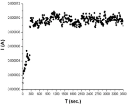
enhancement factor is β ~ 4993 as shown in Fig. 4. The I-T curve of CNCs is depicted in Fig. 5, where under the 900 V applied bias and the spacing among the specimen and anode is 100 µm during measure time 3600 sec. The result shows the CNCs with emission ~10 µA for 3600 seconds operation is stable. The result also indicates the CNCs can bear intense electric field of long time operation.
4. Conclusion
The well-aligned carbon nanotubes and carbon nanocones were successfully synthesized by MPCVD method. The structures of the nanostructures could be varied by manipulating the gas composition, the applied bias, deposition time, plasma pretreatment and plasma post-treatment. On CNTs properties, the best FE properties of the as-grown well-aligned CNTs are Eto ~
as-grown CNTs under the applied field is poor due to weak adhesion with the substrate. On CNCs properties, the best FE properties of well-aligned CNCs were synthesized under H2/CH4 (80/5 sccm/sccm)
source gases with -300 V applied bias for 10 min. It exhibits Eto ~ 5.0 V/µm, Eth ~ 6.99
V/µm, β ~ 4993, and J ~ 173.42.7 mA/cm2
at 10 V/µm, which are much better than CNTs, in addition to a significant increase in stability under the applied electrical field.
References
[1] Iijima, S, Nature, 354, (1991), 56-58. [2] Jang, J., S. J. Chung, and H. S. Kim,
Appl. Phys. Lett., 79, (2001), 1682-1684. [3] Tsai, C. L., C. F. Chen, C. L. Lin, Appl.
Phys. Lett., 80, (2002), 1821-1822. [4] Huang, C. J., Y. K. Chih, J. Hwang, J.
Appl. Phys., 94, (2003), 6796-6799. [5] Hiura, H., T. W. Ebbessen, J. Fujita, K.
Tanigaki and T. Takada, Nature, 367 (1994) 148-151.
5
Fig. 1 Morphologies of well-aligned CNTs under various applied bias (a) 0 V (b) -50 V (c) -150 V (d) -250 V
Fig. 2 The I-V curves of as-grown CNTs under different applied bias.
Fig. 3 Morphologies of as-grown CNCs under different negative applied bias (a) 0 V (b) -50 V (c) -150 V(d) -200 V (e) -300 V
Fig. 4 J-E curve of as-grown CNCs under -300 V applied bias.
Fig. 5 I-T curve of as-grown CNCs under applied bias of -300 V
光記錄媒體材料、性質及其應用於光碟記錄容量提升之研究(3/3)
A Study of Optical Recording Media, Properties and Their
Applications to Increase the Storage Capacity of Optical Disks (3/3)
一、 中文摘要
本年度之研究包含:(1)利用第一年完成之 CdSe-SiO2微晶玻璃(Semiconductor-doped Glass,SDG)
製作光碟之遮罩層(Mask Layer)及(2)ZnO-SiO2 SDG 薄膜之白光發射性質研究。在光碟之遮罩層部
分,將 CdSe-SiO2 SDG 導入光碟中後,其在 Pr = 4 mW 時可解析 69 nm 之記號,且訊號雜訊比
(Carrier-to-Noise Ratio,CNR)達 13.56 dB;對 100 nm 之解析 CNR 更可達 40 dB;重複讀取試驗 (Cycleability Test)顯示 CdSe-SiO2 SDG 遮罩層可耐 105次以上之讀取。ZnO-SiO2 SDG 薄膜之白光發射
性質研究部分,光激光譜(Photoluminance,PL)分析顯示其白光光譜由紫外光(420 nm)、藍光(470 - 495 nm)與黃光(560 - 585 nm)組成,藍光發射之性質應肇因於 SDG 膜中眾多之 ZnO/SiO2界面,其使
空乏區(Depletion Layer)之寬度增加,藍光發射之強度因而增強,其與既有之黃光恰組合成白光光譜。 關鍵詞:CdSe-SiO2微晶玻璃、遮罩層、ZnO-SiO2微晶玻璃、白光發射性質。
Abstract:The research items included in this year are: (1) the application of CdSe-SiO2 SDG layer as the mask
layer material for optical disk and (2) the white-light emission property of ZnO-SiO2 SDG thin film. In the part
related to optical disk recording, it was found that the 69-nm marks could be consistently retrieved at reading power Pr = 4 mW with carrier-to-noise ratio (CNR) = 13.56 dB. The signals were clearly resolved with CNRs
nearly equal to 40 dB at Pr = 4 mW when the recorded mark sizes were over 100 nm. The cycleability test
indicated that the CdSe-SiO2 SDG layer might serve as a stable and reliable optical mask layer in 105 readout
cycles. In the part related to white-light emission property of ZnO-SiO2 SDG thin film, the PL measurements
showed that the ZnO nanoparticles embedded in the SiO2 matrix emit white-light consisting of violet (420 nm),
blue (470 - 495 nm), and yellow (560 - 585 nm) emissions. The presence of the blue emission was attributed to the large amount of ZnO/SiO2 interfaces, which enlarges the depletion layer width and then enhances the related
transition.
Keyword: CdSe-SiO2 SDG Layer, Mask Layer, ZnO-SiO2 SDG Layer, White-light Emission Property .
二、緣由與目的 數據資料之儲存與取用是當今資訊產品使用中的重要部份。現行資料之儲存可分為磁記錄與光記錄 兩大類,光記錄通常以雷射光進行資料之記錄,是當今資料儲存最熱門、最重要的產品。 光碟研究的重要方向包括提高資料傳輸速率與提升記錄密度,使用短波長之藍光雷射與高數值孔徑 (Numerical Aperture,NA)之物鏡的讀寫頭為改善之方法之一[1],但高功率之藍光雷射二極體目前仍 有諸多困難,在光碟中加入適當之遮罩層材料,利用超解析效應(Super-resolution Effect)因此成為突破 光學繞射極限(Diffraction Limit)以提高記錄密度的另一項選擇。超解析效應最早由 Tominaga 等人在光 碟中加入15 nm 的銻(Sb)而發現其能解析 90 nm 之訊號[2];此一現象並已被應用到磁光與光記錄媒體 之中[3-4]。近幾年其它之材料系統,如 AgOx[5]與 PtO2[6]之柰米微粒、ZnO[7]、CdSe[8]等亦呈被證實其
保概念;而LED 除兼具有輕薄短小、壽命長、省電、高發光效率等的優點之外,還可與半導體、微光機 電元件整合,進而提升資訊產品的智慧型功能。白光LED 則是未來世代最重要且必然的發展趨勢,白光 LED 源起於 1994 年 Nakamura 發表了高功率量子井結構的藍綠光 GaN LED[9]與日亞化學(Nichia)於 1996 年 9 月推出第一個以 GaN 藍光激發 YAG(580 nm)黃光螢光粉的白光 LED[10]。GaN LED 雖可達 到高功率的要求,但其無適當晶格常數匹配的基板與 p-GaN 成長困難,仍舊無法簡化製程上的繁複步驟, 在顯示器背光源的應用層面亦受到侷限,主要原因在於藍光激發光與黃光螢光粉的混光及亮度均勻性仍 有待考量,因此新技術趨勢則傾向以外部量子效應(External Quantum Efficiency)超過 20%的 UV LED 做為激發光源[11-12]激發三原色螢光體,以期達到最佳的混色效果,而除了採用已成功研發的 GaN 做為 活化區(Active Region)外,ZnO 則被視為最具發展潛力的發光層材料。
柰米尺度之ZnO 已知具備異於塊材之光發射性質[13-14],溶凝膠法(Sol-gel Process)[15]、分子 批覆法(Molecular Capping)[16]與浸沒法(Impregnation)[17]等方法曾被應用以在氧化矽或高分子基材 內製成奈米尺度之ZnO 微粒,本實驗則以貼靶濺鍍法製備 ZnO-SiO2 SDG 薄膜,並研究其白光發射之性
質。
三、實驗方法
(1)以 CdSe-SiO2 SDG 製作光碟之遮罩層部分:利用自組的濺鍍系統在 PC 基板上依序鍍成架構為
Zns-SiO2 (130 nm)/CdSe-SiO2 SDG (60 nm)/Zns-SiO2 (25 nm)/Ge2Sb2Te5 (20 nm)/Zns-SiO2 (20 nm)之光碟結
構,以動態測試儀(DDU-1000,Pulstec Industrial Co.)定出最佳之寫入(Pw)與讀取(Pr)雷射功率,
再進行其超解析效應與重覆讀取能力之量測。光碟之微觀結構則以電子顯微鏡(Transmission Electron Microscopy,Philips Tecnai 20 TEM)觀察之。
(2)ZnO-SiO2 SDG 薄膜之白光發射性質研究部分:將不同面積的 ZnO 圓碇置於石英靶材上,以 RF 濺 鍍法製成約140 nm 厚的薄膜,再分別以電子顯微鏡(TEM)分析其微觀結構,以 X 光發射光譜儀(X-ray Photoemission Spectroscopy,XPS)分析其成分,PL 光譜儀則用以分析其發光光譜之組成。 四、結果與討論 (1)以 CdSe-SiO2 SDG 製作光碟之遮罩層部分: 圖一所示為不同長度的訊號在 Pr = 1 ∼ 4 mW 之 CNR 值比較。以 Pr = 4 mW 讀取 69 nm 長的訊號時, CNR 可達 13.56 dB;圖一同時顯示對 100 nm 之解析 CNR 更可達 40 dB。因本實驗之讀取系統的雷射光 點直徑約為1 µm,其解析極限約為 270 nm;依繞射解析之理論分析之,在遠場光學之讀取條件下,其 不可能解析四分之一大小以下之訊號,而69 nm 恰約為 270 nm 之四分之一,而其也為以同一讀取系統 利用超解析效應讀取之最小訊號長度。 重複讀取實驗係以 Pr = 4 mW 取 96 nm 長之訊號之 CNR 值變化,其結果如圖二所示。除因殘熱效 應造成CNR 略為下降之外,在 105次的讀取中,CNR 均維持在 35 dB 以上,故 CdSe-SiO 2 SDG 有潛力 成為一可靠且有效之遮罩層材料。 第一年之研究已顯示CdSe-SiO2 SDG 薄膜具備高熱吸收之特性,Z-scan 試驗亦證實其具有 40%之
穿透率變化之性質,我們初步歸因於CdSe-SiO2 SDG 膜之超解析行為應來自於熱效應(Thermal Effect),
其藉吸收部份之雷射光能量造成光點之縮小,故可鑑別小於繞射極限之訊號。 (2)ZnO-SiO2 SDG 薄膜之白光發射性質研究部分: 圖三為不同ZnO 含量之 ZnO-SiO2 SDG 薄膜之微觀結構,表一則為 XPS 之成份分析結果;XPS 結 果顯示低ZnO 含量試片中 Zn 之氧化較為完整。圖四為 PL 光譜圖,其顯示低 ZnO 含量之試片 A ∼ D 具 備白光發射之性質。Lorentzian 曲線分析顯示白光光譜由紫外光(420 nm)、藍光(470 ∼ 495 nm)與黃 光(560 ∼ 585 nm)組成,在 ZnO 含量小於 40 wt.%以下時,藍光與黃光之發射強度大約相當;大於 40 wt.% 時則以黃光為主。
圖五為ZnO 之能帶模型。點線代表自淺施體能階(Shallow Donor Level)至氧空缺( ••
O
V )之遷移
所產生之黃光發射光譜,長斷線則代表傳導帶(Conduction Band,CB)至鋅空缺(V ′Zn)所產生之藍光
發射光譜,因鋅空缺為Vanheusden 等人所提出之空乏區效應(Depletion Effect)之主要之缺陷[18],當 奈米尺度之ZnO 被植入 SiO2中時,所產生之眾多界面使空乏區寬度增加,此同時增加CB → V ′Zn之遷移
比率,藍光之發射也因此增強,與既有之黃光光譜恰組成白光發射光譜。
五、計畫成果自評
本年度以第一年完成之CdSe-SiO2 SDG 薄膜應用於光碟遮罩層之製作,其可解析 69 nm 的記錄訊
號,超越目前其它遮罩層材料解析 90 nm 訊號之報導,本研究成果已獲 2005 年於美國夏威夷所舉辦 ISOM’05 會議接受,並將轉載發表於 Jpn. J. Appl. Phys.,專利申請亦已提出;(iii)SDG 薄膜之摻雜為 ZnO 奈米顆粒時能發出白光,具備應用於白光 LED 之潛力,此部分之發光機制與試片之發光再現性之 分析已大致完成,目前正整理並撰寫期刊論文中。如能以ZnO-SiO2 SDG 薄膜為基礎完成白光 LED 之製
作,對能源產業將有所貢獻。
六、參考文獻
[1] A.B. Marchant, “Optical Recording – A Technical Review”, Addison-Wesley, (1990). [2]J. Tominaga, T. Nakano and N. Atoda, Appl. Phys. Lett., 37, 2078(1998).
[3] H. Awano, H. Shirai, H. Watanabe, K. Shimazaki, M. Yoshihiro and N. Ohta, Technical Digest of Joint
MORIS/ISOM’97, Yamagata, Japan, October, 1997, p. 262.
[4] T. Shintani, K. Moritani, A. Hirotsune, M. Terao, H. Yamamoto and T. Naito, Technical Digest of Joint
MORIS/ISOM’97, Post-Deadline Papers, Yamagata, Japan, October, 1997, p. 21.
[5] J. Tominaga, H. Fuji, A. Sato, T. Nakano and N. Atoda, Jpn. J. Appl. Phys., 39, 957(2000). [6] T. Kikukawa, T. Nakano, T. Shima and J. Tominaga, Appl. Phys. Lett., 81, 4697(2002). [7] T. Kikukawa, A. Tachibana, H. Fuji and J. Tominaga, Jpn. J. Appl. Phys., 42, 1038(2003). [8] T. Nagase, S. Ashida and K. Ichihara, Jpn. J. Appl. Phys., 38, 1665(1999).
[9] S. Nakamura and M. Senoh, Appl. Phys. Lett., 67(13)(1995), p.1868. [10] 紀國鐘、蘇炎坤,“光電半導體技術手冊”,民國 91 年 10 月。
[11] K.H. Kim, Z.Y. Fan, M. Khizar, M.L. Nakarmi, J.Y. Lin and H.X. Jiang, Appl. Phys. Lett.,
85(20)(2004), p.4777.
[12] C.C. Pan, C.M. Lee, J.W. Liu, G.T. Chen and J.I. Chyi, Appl. Phys. Lett., 84(25)(2004), p.5249. [13] L. Jing, Z. Xu, J. Shang, X. Sun, W. Cai, and H. Guo, Materials Science and Engineering, A332, 356(2002).
[14] K. Vanheusden, W. L. Warren, C. H. Seager, D. R. Tallant, and J. A. Voigt, J. Appl. Phys., 79, 7983(1996). [15] H. He, Y. Wang, and Y. Zou, J. Phys. D: Appl. Phys. 36, 2972 (2003).
[16] L. Guo, S. Yang, C. Yang, P. Yu, J. Wang, and W. Ge, and G. K. L. Wong, Appl. Phys. Lett. 76, 2901 (2000).
[17] C. Cannas, M. Mainas, A. Musinu, and G. Piccaluga, Composites Science and Technology 63, 1187 (2003). [18] K. Vanheusden, W. L. Warren, C. H. Seager, D. R. Tallant, and J. A. Voigt, J. Appl. Phys., 79, 7983(1996).
450 400 350 300 250 200 150 100 50 Mark size (nm) 0 10 20 30 40 50 60 70 CN R (dB) Pr=1mW Pr=2mW Pr=3mW Pr=4mW When Pw = 26 mW Resolution limit 圖一、不同長度的訊號在 Pr = 1 ∼ 4 mW 之 CNR 值比較。 1 10 100 1000 10000 100000 Readout cycle 0 10 20 30 40 50 CN R (dB) Pw = 26 mW; Pe = 6 mW Mark size ≈ 96 nm 圖二、重複讀取實驗結果。
圖三、不同ZnO 含量之 ZnO-SiO2 SDG 薄膜之微觀結構。 圖三、不同ZnO 含量之 ZnO-SiO2 SDG 薄膜之 PL 光譜。 0 200 400 600 800 Sample B 547 469 419 200 400 600 800 1000 Sample A 561 463 409 300 400 500 600 700 800 0 200 400 600 800 Sample C 547 470 419 Int ensit y (a .u ) Wavelength (nm) 300 400 500 600 700 800 0 4000 8000 12000 Sample F 587.8 495.9 0 5000 10000 15000 20000 25000 Sample E 586.1 495.9 Wavelength (nm) Int ensit y (a .u ) 200 400 600 555.3 Sample D 467.0 420.6
圖五、ZnO 之能帶模型。
表一、ZnO-SiO2 SDG 薄膜 XPS 分析結果。
Binding energy (eV) Sample t (nm) ZnO (wt.%) Zn2p1/2 Zn2p3/2 Si2p O1s A 154 4.92 1048.4 1025.4 106.2 535.6 B 132 9.79 1047.4 1024.4 105.2 534.6 C 124 14.84 1047.0 1023.8 104.2 533.6 D 128 41.54 1046.6 1023.6 103.8 533.0 E 136 47.18 1046.4 1023.4 103.0 532.8 F 147 52.63 1046.4 1023.2 102.8 532.8 ' Zn V '' Zn V • O V • • O V ~ 3.35 eV ~ 0.7 eV ~ 2.0 eV ~ 2.8 eV Valance Band • • • i i Zn Zn / 0.2 ~ 0.5 eV ~ 2.2 eV Conduction Band
奈米結構氧化物晶體材料製程與光電特性研究(3/3)
Synthesis and optical properties of patterned ZnO nanorods and
ZnS-ZnO core-shell nanotube arrays
中文摘要 本研究延續先前的研究工作,來進行 ZnO nanorods 圖案陣列化與成長製程 與光電特性研究。並進行ZnS-ZnO core-shell 之異質界面奈米管(nanotubes) 的製程研究與光電發光性質探討。首先 主要是在探討在不同熱處理基版上的 ZnO 奈米柱的成長行為和微結構的發 展。 隨著不同的熱處理,規則排列的 ZnO 奈米柱則會直接從 ZnO film 上沿 著[0002]方向成長。並可經由基板上 ZnO 晶粒結構及形狀的改變,來控制及 成出具有不同長寬比與型態的 ZnO nanorods。在另外一方面,進而利用利 用原子層化學氣相沉積技術,在陽極氧 化鋁模板中製備氧化鋅奈米管陣列。並 可藉由後續熱處理步驟來降低缺陷含 量,提升氧化鋅奈米管之光學性質。並 可調控氧化鋅奈米管陣列的管壁成長 厚度,使其在光激發光性質上產生具有 共振效應,可進一步提升紫外光發光強 度。當若將氧化鋅奈米管陣列以硫化鈉 水溶液進行硫化,可得到硫化鋅–氧化 鋅的核–殼奈米管結構。經由 XPS 分析 可以證明表層的氧化鋅已轉變為硫化 鋅,形成核–殼結構之奈米管。硫化鋅 的形成可能消除部份的缺陷,並伴隨著 量子尺寸效應,使核–殼結構之光學性 質較氧化鋅奈米管提升約 6 倍,未來可 應用於發光元件或平面顯示器技術上。 關鍵字: ZnO 奈米柱、圖案陣列化、硫 化鋅–氧化鋅的核–殼奈米管結構、光
substrate annealed at different temperatures was first studied. HRTEM observation demonstrates that both ZNs and ZnOf on Si
substrate are coherent. Subsequently, AAO was used as template to deposit ZnO nanotube by atomic layer deposition (ALD) process. After sulfurating, hetrostructured ZnS-ZnO core-shell nanotube arrays with the diameters of 50-80 nm and lengths up to 1 µm have been successfully developed. It is found that the crystal growth orientation of the ZnO layer was strongly dependent on the substrate temperature. Furthermore, transmission electron microscopy (TEM) reveals that ZnO nanotubes show a good uniformity in thickness due to the self-limiting feature of atomic layer deposition (ALD). X-ray photoelectron spectroscopy (XPS) analysis indicates that the binding energy of S 2p is the same as that of bulk single-crystal ZnS, and the Zn 2p3/2 peak is shifted about 0.5 eV due to the formation of Zn-S bonds. Photoluminescence (PL) shows the relative intensity ratio of ultraviolet (UV) emission to deep level emission for ZnS/ZnO core-shell can be enhanced as 9 times as that of original ZnO nanotube.
Keywords: ZnO nanorods ; Patterned allay ; ZnS-ZnO core-shell nanotube ; Optoelectronic properties ; Microstructure evolution;well-aligned
I. Introduction
One-dimensional (1D) nanostructures have great potential for learning the fundamental concepts of the roles of both dimensionality and size in physical properties as well as for application in nanodevices and functional materials. Other than carbon nanotubes, 1D nanostructures
13
Growth of 1D ZnO nanostructures including nanotubes,[2] nanowires,[3] , nanorods[4] , and nanobelts[5] have been also developed. Such nanostructures enable the observation of unique optical optical confinement and microcavity. So far, many works have been done to investigate optical cavity effect within nanostructure such as nanowires and nanorods). However, many research groups have found that the non-passivated surface sites may act as either a deep level recombination and suppress efficient luminescence, especially in ZnO nanorods. [6,7]
The passivation of materials by wider band-gap inorganic materials could provide effective elimination of surface-related defect states and a confinement of charge carriers into the core material due to the band offset potential. Song et al.[8]
reported that ZnSe/ZnS core/shell nanocrystal showed a 2000% enhancement of luminescence quantum yield compared to bare ZnSe nanocrystals. Therefore, in this work, we developed a process to synthesize ZnS/ZnO Core-Shell nanotubes with controlled relative wall thickness of ZnS to ZnO. First, anodic aluminum oxide (AAO) was used as templates to deposit thin ZnO nanotubes by atomic layer deposition (ALD) process[9]
and then a sulfurating method was employed for the synthesis of ZnS/ZnO core-shell nanotubes. In addition, optical properties of ordered ZnS/ZnO core-shell nanotubes arrays are also characterized.
II. Experimental
Both precursors of methenamine
(C6H12N4) and zinc nitrate hexahydrate
(Zn(NO3)2.6H2O) were used for preparing
the solution to grow ZnO nanorods (ZNs). The ZnO thin films were deposited on Si substrates by RF magnetron sputtering. The annealed ZnOf/Si substrates were placed
inside the aqueous solution at 75oC for 10 hours. After that, the ZnO nanorods were vertically grown on the substrates. On the other hand, the ZnO nanotubes were fabricated by an ALD process on Si substrate with AAO template.[10] Diethylzinc (DEZ) and H2O reactant gases were alternately fed into the growth chamber with nitrogen as a carrier gas. The inner wall of ZnO nanotubes were sulfurated by 50 mL of 0.8 M Na2S solution. The resulting
core-shell nanotubes were cleaned and then dried in an isothermal oven at 70oC. The morphology of ZnS-ZnO core-shell nanotubes was examined by scanning electron microscopy (SEM) and transmission electron microscopy (TEM). The crystal structure was determined using X-ray diffraction (XRD) with CuKα radiation.
Energy-dispersive X-ray spectroscopy (EDS) and X-ray photoelectron spectrometer (XPS) were used for the composition analysis of the ZnS-ZnO core-shell nanotubes. Photoluminescence measurement was performed by the excitation from 325 nm He-Cd laser at room temperature.
III. Results and discussion
A: Synthesis and Optical Properties of Patterned ZnO nanorods
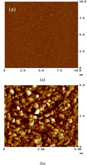
Figure 1 shows the atomic force microscopy (AFM) images of the ZnO film coated on Si substrate (ZnOf/Si) with
different annealing temperatures. The grain size of the ZnO film increases with increasing annealing temperature. Furthermore, it can be observed in Fig. 1(b)
that many abnormally large ZnO grains were grown on the ZnOf/Si substrate annealed at
800oC in Fig. 1(b). Figure 2 shows the SEM images of the ZNs grown on the patterned ZnOf/Si annealed at different temperatures.
A patterned ZnO film on Si substrate was fabricated by photolithography and etching process. As the patterned ZnOf/Si substrate
was placed into the aqueous solution to grow ZNs, well-aligned ZNs are grown on the designed substrate as shown in Fig. 2(a) and this demonstrates the selected growth behavior of the ZNs. Figure 2(b) shows the surface images of large-scale arrayed ZnO nanorods grown on the patterned ZnOf/Si at
room temperature. It was found that the ZnO nanorods have a well-defined hexagonal plane with a homogeneous diameter. As the patterned substrate was first annealed at 600oC and 800oC, and then grown in the solution at 75oC, it was found that the morphology of the ZNs was remarkably changed as shown in Fig. 2(c) and (d), especially for the ZnOf/Si annealed at 800oC.
Furthermore, the dimension of ZNs increases with increasing annealing temperature. The average dimension of the ZNs is 20 nm and 300 nm in diameter for the ZnOf/Si at room temperature and
annealed at 800oC, respectively. As compared with the AFM images of ZnO film on Si substrate in Fig. 1, it seems to imply that the growth behavior of the ZNs is correlated with the grain size of the ZnO film coated on Si substrate as illustrated in
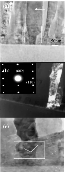
Figure 4(a) shows the TEM bright-field (BF) image of the aligned ZNs grown on ZnOf/Si substrate annealed at 600oC. It was
observed that most of the ZNs were grown in a direction perpendicular to the ZnOf/Si
substrate. The TEM dark-field image in Fig. 4(b) reveals TEM dark-field image marked with arrows in the fig. 4(a) that there was a close relationship between ZNs and ZnO film. Both ZNs and ZnOf on Si substrate
were grown along the same direction of [0002] and are coherent as demonstrated in the selected-area electron diffraction pattern(SAED) (inset of Fig. 4(b)). In addition, as one pays attention to the interface between ZNs and ZnOf/Si shown
in Fig. 4(c), the HR-TEM image in Fig. 4(c) (magnified from the marked area in Fig. 4(a)) reveals that both well-aligned ZNs and ZnO film have identical parallel lattice fringes. The ZNs seem to nucleate from the concave tip near the grain boundary (marked as lines) between two ZnO grains in ZnO film.
As the ZnOf/Si substrate was annealed at
800oC, a low-magnification TEM image of the ZNs was shown in Fig. 5(a). The HR-TEM image of the ZNs in Fig. 5(b) (marked with frame in Fig. 5(a)) indicates that some nanorods are merged together to form a larger ZN along similar growth direction [0002].[11] The SADP (shown in the inset in Fig. 5(b)) reveals the split of diffraction spots with several degree differences. This suggests that the larger ZNs are not perfect single crystalline and
15
the larger ZnO nanorods can be considered from direct combination of a small number of individual nanorods which was similar to oriented attachment.
B: Synthesis and Optical Properties of Patterned ZnS-ZnO Core-Shell Nanotube Arrays
The SEM images of bare AAO and ZnO nanotubes array in AAO template are presented in Fig. 6. The thickness of the fabricated AAO is about 1 µm, and the channel diameter is less than 100 nm. After the ZnO thin-film was deposited into the channels of AAO by ALD (Fig. 6(b)), the diameter of the channel is about 50-80 nm. EDS (inset of Fig. 6(b)) analysis of the nanotubes in AAO template shows that the nanotubes are mainly composed of Zn and O.
XRD spectra were obtained from nanotube arrays with various substrate temperatures, as shown in Fig. 7. The [002] orientation was observed at low substrate temperatures. It was found that [002] orientation would become dominant with increasing the substrate temperature, indicating that the c-axis is parallel to the prefer orientation of wurtzite ZnO. It was believed that the orientation of ZnO nanotubes strongly depends on the substrate temperature. Since [002] is the preferred orientation of wurtzite ZnO, ZnO thin film will grow along the c-axis at higher temperature, suggesting that the crystal structure of the ZnO nanotubes can be controlled.
The optical properties can be enhanced by reducing defect concentration through post-annealing processes. As shown in Fig. 8, the intensity of UV emission at 380 nm can be doubly enhanced. In addition, resonance effects are also observed from
highly arrays of ZnO nanotubes as compared to ZnO film. Several weak peaks periodically appear at 400~ 600 nm. It was believed that this resonant phenomenon is strongly related to the wall thickness of ZnO nanotubes. Because in our experiment, it was found that this resonant phenomenon only appear at a specific wall thickness as because as increasing deposition of ZnO film on the AAO template, the wall thckness of ZnO nanotubes will be increased, thus causing a decreased size in hollow tube. With the decrease in inner size of ZnO nanotube up to a specific size, microcavity was probably formed, which leads to an enhanced UV emission intensity and resonant peaks.
The chemical state of atoms on the surface was analyzed by XPS analysis. A comparison of the XPS spectra recorded from the as-synthesized ZnO nanotubes and the ZnO-ZnS core-shell nanotubes is shown in Fig. 9. The XPS analysis shows the nanotubes are mainly composed of Zn, O, and S. Figure 9(a) reveals the signal of S 2p in the ZnO nanotubes with and without sulfurating. The binding energy of S 2p appears at about 162 eV after sulfuration, which is close to the value of bulk ZnS.[12] Figure 9(b) shows the XPS data of Zn 2p3/2 in ZnO nanotubes and ZnO-ZnS core-shell nanotubes. For ZnO nanotubes, the binding energy of Zn 2p3/2 remains at 1022.8 eV, which is larger than the value of Zn in bulk ZnO. The status of Zn 2p3/2 peak in ZnO film was confirmed by Chen et al. [13] The binding energy of Zn 2p3/2 in ZnS is about 1021.9 eV, which is smaller than the value of Zn 2p3/2 in ZnO. The Zn 2p3/2 peak in the sulfurated ZnO nanotubes is shifted toward a lower binding energy around 0.5eV, implying that some of Zn-O bonds were transferred into Zn-S bonds.
Figure 10(a) shows the TEM image of ZnS-ZnO core-shell nanotubes, with ZnO as the shell and ZnS as the core in the nanostructured AAO template. However, the ZnS surface is not smooth because the lattice constants of zinc-blend ZnS (a = 0.54109 nm) and wutzite ZnO (a = 0.3249 nm and c = 0.52065 nm) are incompatible. Thus, the substitution reaction was unlikely to produce well-structured ZnS, especially the reaction at room temperature. The wall thickness of ZnO nanotube is about 35-50 nm, and that of ZnS layer is smaller than 10 nm (Fig. 10(a)). Selected-area electron diffraction (Fig. 10(b)) recorded from the core-shell nanotube reveals two sets of ring diffraction patterns which fit very well to zinc-blend structure ZnS and wurtzite structure ZnO. Therefore, it indicates that both crystal structures of core and shell were poly-crystalline ZnS and ZnO.
The photoluminescence (PL) property of the ZnO-ZnS nanostructures was measured as shown in Fig. 11. A small shift of ~1.5nm for the ZnO-ZnS nanostructure was observed that is possibly due to the reduced size of the ZnO nanotubes,11 especially in the thickness direction of the nanotubes. Moreover, it was found that the intensity of the UV emission increases but green light emission decreases after sulfurating reaction. The weakness in green emission presumably resulted from suppression of nonradiative recombination due to reduced concentrations of surface states. In contrast, the UV emission is strong due to the fact that most of the excited electron-hole pairs relax radiatively at the passivated surface states.[14] Therefore, the relative ratio of the intensity of UV emission
enhanced by 9 times compared to that of original ZnO nanotubes.
IV. Conclusion
It is demonstrated that the growth of patterned ZnO nanorods is controlled by annealing ZnOf/Si substrate at different
temperature. When the ZnOf/Si substrate
was annealed to crystallize ZnO phase, both ZNs and ZnOf on Si substrate were found to
be coherent. The ZNs seem to nucleate from the cup tip near the grain boundary between two ZnO grains in the ZnO film. However, a higher annealing temperature may lead to the formation of a larger ZnO crystal due to coplanar coalescence behavior of several individual ZnO nanorods. On the other hand, using AAO as a template, ZnS-ZnO core-shell nanotubes have been synthesized for the first time by atomic layer chemical vapor deposition technique into AAO template along with the sulfurating the ZnO nanotube array using Na2S solution. The inner and wall thickness of ZnS-ZnO core-shell nanotubes are smaller than 10 nm and about 35-50 nm, respectively. A small blue shift was observed in the PL spectrum from the ZnO-ZnS core-shell nanotubes, possibly caused by a small quantum-confinement effect. Moreover, surface passivation of ZnO nanotubes by a wider band gap material, ZnS, lesds to suppressed nonradiative recombination and significantly enhanced luminescence intensity.
17
the National Science Council of the
Republic of China, Taiwan under Contract No. NSC-93-2216-E-009-005.
References
[1] D. P. Norton, Y. W. Heo, M. P. Ivill, K. Ip, S. J. Pearton, M. F. Chisholm, and T. Steiner, Materialstoday, 34 (2004)
[2] Y. J. Xing, Z. H. Xi, Z. Q. Xue, X. D. Zhang, and J. H. Song, Appl. .Phys. Lett., 83, 1689
(2003).
[3] M. H. Huang, Y. Wu, H. Feick, N. Tran, E. Weber, and P. Yang, Adv. Mater., 13, 113
(2001).
[4] J.-J. Wu and S.-C. Liu, Adv. Mater., 14, 215 (2002).
[5] Z. W. Pan, Z. R. Dai, and Z. L. Wang, Science, 291, 1947 (2001).
[6] E. G. Bylander, J. Appl. Phys., 49, 1188 (1978).
[7] D. Li, Y. H. Leung, A. B. Djuri i , Z. T. Liu, M. H. Xie, S. L. Shi, S. J. Xu, and W. K. Chan,
Appl. .Phys. Lett., 85, 1601 (2004).
[8] K. Song and S. Lee, Current Appl. Phys., 1, 169 (2001).
[9] H. J. Shin, D. K. Jeong, J. G. Lee, M. M. Sung, and J. Y. Kim, Adv. Mater., 16, 1197 (2004).
[10] H. Masuda and M. Satoh, Jpn. Jour. Appl. Phys., Part 1 35, L126 (1996).
[11] Bin Liu and Hua Chun Zeng, J. Am. Chem. Soc., 125, 4430 (2003)
[12] J. F. Xu, W. Ji, J. Y. Lin, S. H. Tang, and Y. W. Du, Appl. Phys. A 66, 639 (1998).
[13] M. Chen, X. Wang, Y. H. Yu, Z. L. Pei, X. D. Bai, C. Sun, R. F. Huang, and L. S. Wen, Appl. Surf. Sci., 158, 134 (2000). [14] H. Yang, Appl. Phys. Lett., 82, 1965 (2003).
(a)
(b)
Fig. 1. SEM micrographs of ZnO nanorods
grown on different substrates: (a) Si substrate and (b) ZnOf/Si substrate.
0 100 200 300 400 500 600 700 800 900 10 20 30 40 50 60 70 80 90 100
ZnO thin film ZnO nanorods Temperature(oC) ZnO thin f ilm grain s iz e s (n m ) 50 100 150 200 250 300 ZnO nanorods diam et e r(nm )
Fig. 2. X-ray diffraction patterns of ZnO nanorods grown on (a) Si and (b) ZnOf/Si
substrates.
Fig. 3. Both ZNs diameter and ZnOf grain
size as a function of annealing temperature
Fig. 4 TEM bright-field and (b) dark field images of the aligned ZNs grown on ZnOf/Si substrate annealed at 600oC. A
HRTEM interface image between ZNs and ZnOf is shown in (c) (d) (c) 20μ (a) (b) (002) (110)
(b)
50nm(a)
(c)
19 350 400 450 500 550 600 650 In te n s it y Wavelength (nm) ZnO film ZnO nanotube
Fig. 5. (a) low-magnification TEM images of
ZnO nanorods grown on the ZnOf/Si
annealed at 800oC. (b) HRTEM images of ZnO nanorods in the marked frame of Fig. 5(a) with split diffraction pattern in the inset. HRTEM image of (c) left, (d) middle and (e) right side of the larger nanorod showing it seems to be composed of three ZNs.
Fig. 6. SEM image of (a) AAO template and (b) ZnO nanotubes in AAO with EDS shown in the inset.
Fig. 7. XRD of ZnO nanotube arrays with deposition temperature from 180oC to 270oC.
Fig. 8. Comparison of PL spectra in ZnO film and ZnO nanotubes.
(b
20 20(
(c
(
(e
(
Fig. 9. XPS spectra of (a) S 2p of ZnO nanotube and (b) Zn 2p3/2 of ZnS/ZnO core-shell
Fig. 10. (a) TEM image of ZnO-ZnS core-shell nanotubes.(b) Selected-area electron-diffraction pattern of ZnS/ZnO
Fig. 11. PL spectra of ZnO nanotubes and ZnS-ZnO core-shell nanotubes.
350 400 450 500 550 600 650 Inte nsi ty Wavelength (nm) ZnO nanotube ZnS/ZnO core-shell
21
用晶圓接合與溼式蝕刻方式來剝離側向覆蓋生長之氮化鎵
磊晶層(3/3)
一、摘要 1. 中文摘要 關鍵詞:氮化鎵,晶圓接合,異質磊晶,藍寶石。 本計畫主要的目的在於解決氮化鎵(GaN)薄膜異質磊晶(heteroepitaxial) 於藍寶石(sapphire)基材所衍生的許多問題。期望藉由晶圓接合(wafer bonding),轉移氮化鎵磊晶層於它種基板上。 。 2. 英文摘要Keywords:gallium nitride, sapphire, wafer bonding,.
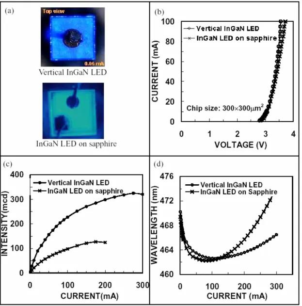
Vertical InGaN-GaN light emitting diodes (LEDs) epitaxial films were successfully fabricated on a 50mm Si substrate using wafer bonding and laser lift-off technology. A high-temperature stable organic film, rather than a solder metal, was used as the bonding agent. It was found that the intensity of the light from the vertical InGaN LED chip was 2.8 times that of the conventional sapphire-substrate LEDs at an injection current of 20 mA. The vertical InGaN LEDs were operated at a much higher injection forward current (280mA) than were sapphire substrate LEDs (170mA). The light-output pattern of the vertical InGaN LEDs is more symmetrical than that of the sapphire-based LEDs. The vertical InGaN LEDs remain highly reliable after 1000 h of testing.
二 、前言及研究目的
The epitaxial growth approaches have considerably increased the brightness of light-emitting diodes (LEDs), and results in rapid advancements in efficiency, the available emission spectrum, the higher power and the application methods. These improvements, coupled with the inherent properties of solid-state devices - low voltage operation, high reliability and low cost - have enabled LEDs to be applied extensively in solid-state lighting and displays. In these applications, LEDs are increasingly replacing conventional technologies.
High-brightness GaN-based light-emitting diodes (LEDs) have attracted considerable attention for their versatile applications in mobile phones, full-color displays and lighting.1-2 Although the development of these GaN-based LEDs is very successful, the poor conductivity of p-GaN limits the performance of LEDs because of current crowding.3-4 This problem can be solved using a thin Ni/Au layer or a highly transparent (> 80%) indium tin oxide (ITO) layer as a current spreading layer.5-6 However, the poor electrical characteristics (electrical resistivity=1011 –1016 ohm-cm) of the nonconducting sapphire substrate are such that the electrodes of the p- and n-metal are both on the top surfaces of the devices. Some of the active layer in the n-contact region is sacrificed. Besides, the heat dissipation of the sapphire substrate is also poor, so the GaN-based LEDs are generally operated at low injection current. These problems can be solved by transferring GaN LEDs on Si 7-8 and Cu substrates 9 to improve the performance and heat dissipation of the devices. Much of this investigation is focused on intermetallic bonding and shows no damage on a small size transfer LED devices. In this work, an n-side-up InGaN LEDs with vertical electrodes was developed by organic bonding. A high-temperature stable organic film, rather than a solder metal, is utilized as the bonding agent to prevent any possible reaction with the metal reflector. The performance and the reliability of the vertical InGaN LEDs were investigated.
三 、研究方法
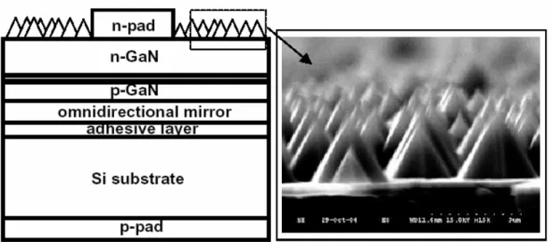
A 50mm sapphire and Si substrates were used. The InGaN-GaN films were grown on a sapphire substrate by low-pressure metalorganic chemical vapor deposition (MOCVD). The LED structures comprise a 0.3 µm-thick Mg-doped GaN, an InGaN-GaN multiple quantum well (MQW) with seven period, a 2 µm-thick Si-doped GaN, a 2 µm-thick undoped GaN layer film and a GaN buffer layer on sapphire substrate. The system of omnidirectional mirrors 10 was then deposited on the InGaN-GaN LEDs to form a p-side contact layer and a reflection layer. This LED wafer was bonded to a silicon substrate covered with a high-temperature stable conductive organic film and a compressive load of 10 kg/cm2. It was then annealed at 200°C for 60 min.
A 50mm InGaN LED wafer was successfully bonded to a Si substrate. The sapphire substrate was then removed by laser lift-off with a frequency-tripled Nd YAG laser at 355 nm 11. No peeling or crack was observed on the bonded sample, revealing that the bonding strength was sufficiently high to exceed the sapphire substrate removing process. The n-GaN roughening surface was obtained by treatment with boiling KOH
23
underside of the Si substrate. Figure 1 presents the structure and the roughened surface. Finally, as shown in Fig. 2, the vertical InGaN LED wafer was successfully cut into isolated devices, each with an area of 300 × 300 µm2. Evidently, the mechanical strength
of the bonding interface was sufficiently high to endure the processes associated with vertical InGaN LEDs.
三 、結果與討論
The vertical InGaN LED devices are easier to process and have advantages over conventional sapphire-based LEDs. The dicing process for vertical InGaN LED devices can replace the complicated process of – dry etching to mesa, laser scribing and breaking of the sapphire-based LEDs. The light emitting area is increased by 15 % because only a single electrode is present on the topside of vertical InGaN LED devices as shown in Figure 3(a). For comparison, standard sapphire-substrate LEDs with an ITO current spreading layer was prepared from the same InGaN-GaN LED epitaxial material. The samples described herein were only cut into chips without encapsulation, before electrical and optical measurements were made.
Figure 3(b) plots the current against voltage (I-V) of LEDs with an area of 300×300 µm2. The vertical InGaN LEDs exhibited normal p-n diode behavior with a forward
voltage of 3.2 V at 20 mA. In this regard, they were similar the conventional LEDs, indicating that neither wafer bonding nor the device process degrades the performance of vertical InGaN LEDs.
Figure 3(c) depicts the effects of injection the current on the luminous intensity of the vertical and conventional InGaN LEDs. The light intensity of the vertical InGaN LED chip is 2.8 times that of the conventional LEDs at an injection current of 20 mA. As presented in Fig. 1, this difference is caused by the improvement of the emission of light from the vertical InGaN LEDs by using only one electrode, the reflection of the downward-traveling light by an omnidirectional mirror, and the roughening of the n-GaN surface. (When the surface of the n-GaN was smooth, the light intensity of the vertical InGaN LEDs chip was double that of the conventional InGaN LED.) Notably, the current can spread uniformly without a thin metal layer (Ni/Au) or a transparent layer (ITO), because the vertical LEDs structure was p-side-down and n-side-up, with an n-metal electrode. Accordingly, the vertical InGaN LEDs do not exhibit the current crowding problem on the top emission area. Therefore, the emission of light is better than that of the conventional sapphire-based LEDs.
Figure 3(c) also reveals that vertical InGaN LEDs can be operated with an injection forward current of 280 mA, which is 170 mA greater than that used in sapphire-substrate LEDs, because the thermal conductivity of Si (168 Wm-1K-1) is 4.8 times higher than that of sapphire (35 Wm-1K-1). However, this improvement in heat dissipation is not as large as was expected because the thermal conductivity of the organic film was poor.
The effects of heat dissipation on the performance of LEDs could be plotted as a peak shift as a function of DC drive current. As shown in Fig. 3(d), when the DC drive current increased from 100 mA to 300 mA, the emission peak wavelengths of the sapphire-based LEDs shifted toward longer wavelengths - from 462.3nm to 474 nm, whereas that of vertical InGaN LEDs on the Si substrate shifted from 462.6nm to 466 nm. These peak shifts were caused by Joule heating.12 Evidently, this Si wafer bonding technique reduced the Joule-heating problem of conventional sapphire-based LEDs.
Figure 4 displays the light-output pattern of the conventional LED and vertical InGaN LED chips. It shows that the light-output pattern of the vertical InGaN LED chip is more symmetrical than that of sapphired-based LEDs, and the power angle of the vertical InGaN LED chip is smaller than that of sapphire-based LEDs, since the vertical InGaN LEDs were designed to have greater extraction efficiency using only one electrode, reflecting downward light, and having a rougher n-GaN surface. Accordingly, most light is easily reflected upward. Additionally, the vertical InGaN LEDs were fabricated by replacing the transparent sapphire substrate with a Si substrate. Thus, only a few photons can be emitted from the side.
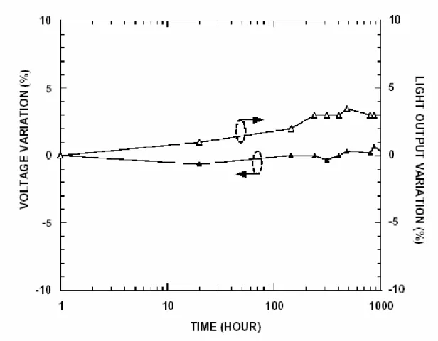
The lifetime of vertical InGaN LEDs was tested at a forward current of 50 mA at 55°C. The voltage variation was under 3% and the output luminescent intensity was not degraded during 1000 h of life testing, as presented in Fig. 5.
三 、未來的方向
(1) 將此技術用在 Cu 基板。 (2) Cu 基板之切割。
25
Fig. 1. (a) Schematic illustration of the vertical InGaN LED structure. (b) the SEM image of roughened surface.
Fig. 2. (a) The OM image of an InGaN LED wafer bonded on a 50mm diameter Si substrate. Wafer was successfully cut into isolated devices with an area of 300 × 300 µm2. (b) the SEM image of the cross section of the LED structure after dicing process.
Fig. 3. The performances of vertical and conventional InGaN LEDs. (a) Top view photograph of the LEDs. (b) Current-voltage (I-V) characteristics of the LEDs. (c) The effects of injection the current on the luminous intensity of LEDs. (d). The peak spectral wavelength as a function of DC drives current of the LEDs
27
Fig. 4. The light-output patterns of (a) sapphire-based LEDs and (b) vertical InGaN LEDs
Fig. 5. Reliability test of vertical InGaN LEDs under stress-condition of 55°C and 50mA.
四 、參考文獻
1 S. Nakamura, M. Senoh, N. Iwasa, and S. Nagahama, Jpn. J. Appl. Phys., 34, L797, (1995). 2H. X. Jiang, S. X. Jin, J. Li, J. Shakya, and J. Y. Lin, Appl. Phys. Lett., 78, 1303, (2001). 3 H. Kim, S.-J. Park, and H. Hwang, IEEE Trans. Electron Devices, 48, 1065, (2001).
4 J. K. Sheu, Y. K. Su, G. C. Chi, P. L. Koh, M. J. Jou, C. M. Chang, C. C.Liu, and W. C.
Hung, Appl. Phys. Lett. 74, 2340 (1999)
5 J. S. Kwak, J. Cho, S. Chae, O. H. Nam, C. Sone, and Y. Park, Jpn. J.Appl. Phys.,Part 1, 40,
6221 (2001).
6 J. K. Sheu, Y. K. Su, G. C. Chi, M. J. Jou, C. C. Liu, and C. M. Chang, Solid-State Electron.
43, 2081 (1999).
7 W. S. Wong, T. Sands, N. W. Cheung, M. Kneissl, D. P. Bour, P. Mei, L. T. Romano, and N.
M. Johnson, Appl. Phys. Lett. 77, 2822 (2000).
8 T. Fujii, Y. Gao, R. Sharma, E. L. Hu, S. P. DenBaars, and S. Nakamura, Appl. Phys. Lett.
84, 855 (2004).
9 Y. K. Song, M. Diagne, H. Zhou, A. V. Nurmikko, C. Carter-Coman, R. S. Kern, F. A. Kish,
and M. R. Krames, Appl. Phys. Lett. 74, 3720 (1999).
10 Donald Huo, M-H Hsieh, W-H Lin, T-F Tseng, J-S Wang and M-J Jou, Compound
Semiconductor. 9 No.11, 31 (2003)
11 M. K. Kelly, O. Ambacher, R. Dimitrov, R. Handschuh, and M. Stutzmann, Phys. Status
Solidi A 159, R3 (1997).
12 D. S. Wuu, S. C. Hsu. S. H. Huang, C. C. Wu, C. E. Lee and R. H. Horng, Jpn. J.Appl.
29
各種型態之奈米碳基材料開發及場發射元件之製作(3/3)
摘要 在場發射的應用上,奈米碳管具有許 多優異的性質,例如能提供高的電流密 度,與相對低的起使電場。然而由於屏蔽 的效應,致使奈米碳管優異的性質無法完 全發揮。研究中利用微波電漿化學氣相沈 積在有金與鎳的矽基板上成長奈米碳管。 由實驗結果可得到獲得密度控制的奈米碳 管,同時具有極佳的准直性。實際的場發 射量測也可證明場發射性質可得到大幅的 改進。 除此之外,由於合成的碳管多少具有 缺陷,或是利用觸媒成長時所殘留的金 屬,因此而限制了碳管在一些方面的應用 及性質。研究中利用兩階段法,在微波消 化系統中使用硝酸及鹽酸可以有效的溶解 觸媒金屬而不會損壞碳管本身的結構,而 整個製成可在一小時內完成,並由熱重分 析可證明金屬的移除效果。 AbstarctCarbon nanotubes (CNTs) have superior properties such as high current density and relative low threshold field in the field emission applications, however, the potential was not totally elaborated due to screening effect. In this study, catalyst composed of gold and nickel was deposited by e-gun evaporation before pre-treatment of furnace annealing. Carbon nanotubes were then grown on silicon substrate using bias-assisted microwave plasma chemical vapor deposition. Vertical aligned carbon nanotubes were grown with gas mixture of methane and hydrogen under external DC bias. The tube structure was confirmed by electron microscopy and the density of carbon nanotubes could be controlled by the
composition of the catalyst. The field emission property was improved greatly with less dense carbon nanotubes.
Also, carbon nanotubes may find their limited use for some applications as they contain a small fraction of metal catalysts in the tubes and tend to have defects along the graphene tube wall. Defects within the multi-walled carbon nanotubes would reduce electrical and structure properties. A two-step acidic treatment in microwave digestion system is used to dissolve metal catalysts. HNO3 or HCl can rapidly absorb microwave heat and energy and completely dissolve metal, which reside in carbon nanotubes without damage. The processing time of the two-step microwave-assisted and acid-treated time to dissolve metal in the MWCNTs is below 1 h. After purification, the amount of residual catalyst metals in samples is estimated by using the thermogravimetric analysis (TGA).
關鍵字: 奈米碳管,場發射,微波消化,化學 氣相沈積
Keywords: Carbon nanotubes, field emission, microwave digestion, chemical vapor deposition
研究內容
A.Density-controlled carbon nanotubes Introduction
It has been reported that field emission from a single multi-walled CNTs reaches 103 A/m2 , which is an order close to the upper limit of the conduction current to 104A/m2. These current densities are far
beyond the field emission current density for practical field emission applications. Efforts have been made to improve the filed emission efficiency of CNTs, which includes purification or doping, but the most effective ways are decreasing the density of the CNTs. Methods like screen printing, anodic aluminium oxide (AAO) and plasma etching were used to tune the field emission behaviour while complicated procedures generates more problems. It has been reported that the density of CNTs plays a significant role in the field emission behaviours, and theoretical value of the optimal CNTs’ density was calculated as 2.5×10⁷ emitters/cm2 [15]. The screening effect varies with the CNTs’ density drastically and the field enhancement is changed. In this study, CNTs’ density can be tuned by varying the catalyst’s composition or size and the density effect is confirmed experimentally.
Experimental details
Nickel and gold film with total thickness of 200 Å was deposited sequentially on Si wafers using an E-Gun Evaporator (model ULVAC EBX-10C, Japan). The specimen was then introduced into a programmable furnace and anneals at a temperature of 900 and ℃ kept for two hours under argon atmosphere and then cooled to room temperature. The pre-treated substrates underwent bias-assisted microwave plasma chemical vapor deposition to grow the CNTs. The microwave power was maintained at
reactive gas of a mixture with H2/CH4=40/10 introduced into the quartz
chamber.
After deposition, the CNTs were characterized using scanning electron microscope (SEM; JEOL JSM-6500F) with an acceleration voltage of 15kV to observe the surface morphology. High resolution transmission electron microscopy (HR-TEM; Philips Tecnai 20) operating at 200kV and energy dispersion spectrum (EDS) was used to observe the nanostructure and the composition of the CNTs. The I-V measurement was taken at a pressure of 10-4 Pa with an indium-tin-oxide glass as anode.
Results and discussion
After furnace annealing, it was shown in figure 1 that the surface roughness increased and the catalyst film tend to form spherical particles as the composition of gold increase due to relief of surface energy. The catalyst particles gradually increased their size from flat surface to hundreds of nanometers in diameter. The increasing of the gold content lead to the decreasing of the nickel-gold alloy melting point and thus the particles size were increasing. It can be seen from the Ni-Au phase diagram that nickel and gold tend to dissolve to each easily, which means that the catalyst particle contains both nickel and gold. Although nickel and gold completely dissolve to each other at 900 and spinodal decomposition ℃ area exists, insufficient cooling rate may
31
not (gold-rich domain).
Fig.1 Surface
morphologies with different film composition of (a) Ni 200Å(b) Ni 150Å ,Au 50Å (c)Ni 130Å, Au 70Å (d)Ni 100Å, Au 100Å, which show different surface roughness. The scale bar in the image is 1µm Fig.2 SEM images of different density of CNTs (a) 2.2×108cm-2 (b) 6.1×107cm-2 (c) 4.7×107cm-2
(d) 3.3×107 cm-2and the insets show the corresponding cross section images. The scale bar in the image is 1µm.
The heat treated surface provided a template for further synthesis of different densities of CNTs. Figure 2 shows the surface morphology of different CNTs density with different heat treatment conditions. The CNTs grew to about 60 nanometers in diameter and several
micrometers in length. Under the same conditions for CNTs’ growth, it was found that the CNTs preferred to grew around the catalyst particles as show in figure 1. It was reported that the island model formatted by pre-treatment of the catalyst was favourable for continuous CNTs’ film growth. The difference is that in this study, the gold or the Ni-Au solutions act as a CNTs growth inhibitor, which means the poor solvability of carbon in gold lead to a minor extrusion of carbon from the catalyst. The density therefore been reduced by the gold content which was unfavourable for CNTs growth and the increasing particle size which leads to fewer growth sites. Also, the bias in the microwave plasma chemical vapour deposition system provided a strong etching effect on the catalyst surface which resisted the CNTs nucleation. However, it was found that the catalyst provided a shield of ion bombardment to the bottom of the particles near silicon surface and nickel rich domains hence initiate the vapour-liquid-solid growth of the CNTs. More precise analyses still needs to be done in this complex system contain elements of silicon, oxygen, nickel and gold. The calculated CNTs densities of figure (a), (b), (c) and (d) are 2.2×108cm-2, 6.1×107cm-2, 4.7×107cm-2 and 3.3×107cm-2, respectively.
Figure 3(a) and (b) shows the TEM images of the CNTs obtained in figure 2 (a) and (c), respectively. The tubular structure with the encapsulated catalyst could be verified. Figure 3(a) shows the curved CNT where some curved CNTs on top of the vertical aligned CNTs could be found in
0 2 4 6 8 10 12 0.0 1.0x10⁻⁴ 2.0x10⁻⁴ (a) 20nm Ni (b) 15nm Ni 5nm Au (c) 13nm Ni 7nm Au (d) 10nm Ni 10nm Au C u rre n t D e n s it y (A /c m 2) Electric Field (V/µm) 0 5 10 15 20 25 2000 2200 2400 En ha n c e m e n t Fa c to r, β x 107 CNTs/cm2
figure 2(a). For the help of the EDS analysis in the TEM system, we found that the catalyst part of the CNTs contained detectable gold composition relative to the nickel. This phenomenon suggested that the gold content of the catalyst resulted in the formation of pentagon and heptagon carbon rings, which due to different carbon solvability and lead to the winding CNTs to compensate the strain. However, the EDS analysis obtained from figure 3(a) shows no detectable gold content was found in the catalyst and straight CNTs were formed by the applied negative bias voltages.
Fig.3 TEM images of the CNTs showing (a) the curved CNT consist of nickel and gold, (b) straight CNT consist of nickel.
In order to examine the effects of CNTs’ density on field emission properties, I-V measurement was utilized. Figure 4 shows the I-V curves measured with different CNTs density. Apparently, field emission efficiency was enormously improved relatively to the sample which continuous CNTs film was present. By decreasing the amount of CNTs, there was
the enhancement factor while too low the density will cause poor emission sites. The best density of CNTs was unable to be acquired from the plot yet which the suggested value of 2.5×107cm-2 is not attainable in this experiment.
Fig.4 Field emission from different densities of CNTs shown in figure 2.
Fig.5 Plot of field enhancement factor versus density of CNTs.
Fowler-Nordheim equations have always been used to describe the relationship between the performance, geometrical parameters and material properties for field emission cases. Under the situation of the same material is used, which means the work function is assumed to be identical, field enhancement factor or the geometrical term, β, is commonly introduced to characterized whether the performance is good or not. The larger the β is, the better the field emission properties
33
with decreasing CNTs densities of 2.2×108cm-2 to 3.3×107cm-2. It was found that the slope of the curve nearly vertical when density of CNTs approached the calculated value of 2.5×107cm-2 from the simulation, and suggested a maxim enhancement factor can get with the density.
Conclusions
In this study, binary system with gold and nickel successfully inhibits the continuous film of carbon nanotubes formation using bias-assisted microwave plasma chemical vapour deposition. The vertical aligned carbon nanotubes can be grown under negative bias voltages and the gold composition contributed to the growth of the curved CNTs. The density of CNTs can be reduced to the value of 3.3×107cm-2 by changing the composition and the heat treatment of the catalyst film. Field emission measurements demonstrate that the experimental value is very close to the reported one of 2.5×107cm-2 and is possible for optimizing field emission efficiency for practical applications.
B. Purification of multi-walled carbon nanotubes by microwave digestion method
Introduction
Many kinds of synthetic techniques have been developed, such as laser ablation, plasma-enhanced chemical vapor deposition, arc discharge, pyrolysis and thermal chemical vapor deposition. Transition metal (e.g. Fe, Co, Ni) particles are known to be
catalysts for vapor grown carbon nanotube synthesis, in which hydrocarbons (e.g. CH4, C6H6) are used as gas source. Metal catalysts are generally necessary to activate carbon nanotube growth. Carbon nanotubes may find their limited use for some applications as they contain a small fraction of metal catalyst in the tubes and tend to have defects along the graphene tube wall. Defects within the multi-walled carbon nanotubes would reduce electrical and structure properties.
Recently, many purified methods have been investigated and have been used successfully to remove impurities from carbon soot. One of the efficient purification methods reported by Tsang et al. was oxidation in air at 750 °C. Due to the small difference in reactivity between multi-walled carbon nanotubes (MWCNTs) and carbon nanoparticles, pure MWCNTs were obtained after prolonged oxidation. Many following up researchers adopted thermal annealing and similar thermal oxidation method to purify CNTs but with low yield.
In this work, a microwave-assisted digestion system was used to dissolve the metal catalyst. Inorganic acids such as H2SO4, HNO3 and HCl can rapidly absorb microwave heat and energy and completely dissolve metals that residue in carbon nanotubes. Since Environmental Protection Agency (EPA) recommended the microwave-assisted method with nitric acid, this leaching procedure of metals has been widely applied in sediments soils and sludge. Nitric acid is strong enough to solubilize
metals from material.
After purification, morphology of carbon nanotubes and degree of purification are evaluated by SEM and TEM. The amount of residual catalyst metals in the samples is estimated by using the thermogravimetric analysis (TGA). A high-yield and no destructive multi-walled carbon nanotubes in high purity are obtained. Metal content is under 5 wt.%.
Experiments
The Co catalyst nanoparticles were deposited on p-type Si (111) wafer by sputtering method. Co catalyst was 7.5 nm in thickness. Experiments took place by electron cyclotron resonance chemical vapor deposition (ECRCVD). Mixture of CH4 and H2 was used as sources gas. Gas flow rates of CH4 and H2 were 18 sccm and 2 sccm, respectively. Power was set at 800 W. The reaction temperature was 600 °C.
An acidic treatment in microwave digestion system (Milestone Microwave Labstation ETHOSD) was used to dissolve the metal catalysts. In this procedure, raw sample of MWCNTs were placed in a 100 ml Pyrex digestion tube. The first digestion step run at 210 °C for 20 min with a 1:1 mixture of 5 M HNO3 and 5 M HCl. The microwave power was set at 100 W. The second digestion step was carried out at 210 °C for 30 min. After digestion, the suspension was filtered with 0.1 mm PTFE (poly-(tetrafluoroethylene)) membrane in
After purification, the morphology of MWCNTs and the degree of purification were observed by TEM. The amount of residual catalyst metals in the samples were estimated with thermogravimetric analysis (TGA) by using a thermal analysis system of Perkin Elmer 1020 Series TGA 7 with a rate of 20 °C/min from 30 to 900 °C at the air flow rate of 10 sccm. Acid treated MWCNTs were oxidized by air at the temperature determined by TGA for 45 min.
Fig. 1: Low magnification TEM image of raw sample.
Fig. 1 shows a low magnification TEM image of raw carbon nanotubes. In this image, there appeared impurities such as amorphous carbons, graphite and metals in multi-walled carbon nanotubes. Metal particles were evident embedded in the tip or in tube core of MWCNTs. Many bundles with a diameter ranging from 10 to 30 nm can be observed in the TEM image.
Fig. 2: Low magnification TEM image of MWCNTs after purification by microwave digestion.
Fig. 2 shows a low magnification TEM image of MWCNTs after purification by microwave digestion. It indicated that most of the metal particles were removed. The