國 立 交 通 大 學
光 電 工 程 研 究 所
碩士論文
量子點面射型雷射動態特性之研究
Dynamical Characteristics of Quantum Dot Vertical
Cavity Surface Emitting Laser
研究生:葉晁恩
指導教授:郭浩中 教授
盧廷昌 教授
量子點面射型雷射動態特性之研究
Dynamical Characteristics of Quantum Dot Vertical
Cavity Surface Emitting Laser
研究生:葉晁恩 Student: Chao-En Yeh
指導教授:郭浩中 教授 Advisor: Prof. Hao-Chung Kuo 盧廷昌 教授 Prof. Tien-Chang Lu
國 立 交 通 大 學
光電工程研究所
碩 士 論 文
A Thesis
Submitted to Institute of Electro-Optical Engineering College of Electrical Engineering
National Chiao Tung University in Partial Fulfillment of the Requirements
for the Degree of Master
In
Electro-Optical Engineering
July 2007
量子點面射型雷射之動態特性研究
研究生:葉晁恩 指導教授:郭浩中教授 盧廷昌教授 國立交通大學光電工程研究所 摘要 本論文主旨在研究量子點面射型雷射的動態特性分析。論文分為兩大部分, 第一部分為 0.98µm 量子點面射型雷射的量測,首先介紹元件的結構與 L-I-V 曲 線。並展示了,在不同溫度下元件的頻率響應、相對雜訊。然後利用校正的方法 求出元件本質的頻率響應,並且分析比較實驗的量測數據。這部份的最近是做元 件非線性失真的觀察和展示在不同溫度下 2.5Gb/s 的眼圖。第二部分為 1.3µm 量 子點面射型雷射的量測,一開始是介紹元件的結構與 L-I-V 曲線。接下來展示分 別在有與無外部注入光源的情況下做,相對雜訊的量測,我們觀察到在有外部注 入光的情況下,雷射共振頻率可以大幅提升,同時我們也對量測相對雜訊的結果 做模擬分析。第一部分的最後是對有量子點與量子井結構的面射型雷射之 Linewidth enhancement factor 做比較與討論。這些成果將有助於面射型雷射 在光通訊的發展。Dynamical Characteristics of Quantum Dot Vertical
Cavity Surface Emitting Laser
Student:Chao-En Yeh Advisor:Prof. Hao-Chung Kuo
Prof. Tien-Chang Lu
National Chiao Tung University
Department of Photonics & Institute of Electro-Optical Engineering
Abstract
In this thesis, we study the dynamical characteristics of quantum dots vertical cavity surface-emitting laser (QD VCSEL). The thesis is divided into two parts. In the first parts, we present the device structure about 0.98µm QD VCSEL. We also present the device structure about 0.98µm QD VCSEL、the L-I&I-V curves、the the relative intensity noise (RIN_ measurement at different temperature、frequency response calibration method、the eye diagram at different temperature and the nonlinear distortion. We also use the calibration method to find the device frequency response. In the second part of this thesis, we report the dynamic characteristics of the1.3µm QD VCSEL、the L-I&I-V curves、RIN measurement of the device with light injection and without light injection、the simulation results of RIN spectrum and linewidth enhancement factor. Comparing with QD and QW structure, we can observer active layers with QD structure having small linewidth enhancement factor at different bias current.
Acknowledgment
(誌謝)
本論文能夠順利完成,首先要感謝我的指導老師郭浩中教授的督促、王興宗 老師和盧廷昌教授的糾正、彭朋群教授的指導,使得我學習到做研究嚴謹的態度 和邏輯的思考以及表達能力的訓練與方法等等。感謝老師們的教誨,兩年的碩士 生涯要過去了,進入半導體雷射實驗室讓我成長了許多,這些過程對我將會是十 分寶貴的經驗。 在這兩年的碩士生活中,彭朋群老師像是學長一樣照顧我,在實驗的過程中 給我方向與指導,在 401 的日子中憲哥和俊榮學長們都很照顧我們這些學弟,帶 給我們很珍貴的回憶,伯駿、柏源、卓木和尚樺都是一起吃飯的好夥伴,帶給我 碩士生活中不一樣的記憶。還有在實驗室共同奮鬥的同學們和博士班學長和學弟 妹們,使我能順利的完成碩士班的考驗。 最後,謹將本論文獻給我的家人。謝謝他們兩年來的支持與鼓勵,使我能 順利完成學位。Contents
Abstract (in Chinese)………...i
Abstract (in English)………...ii
Acknowledgement………..……….iii
Contents………iv
Chapter 1 Introduction 1-1 Introduction of Quantum Dot VCSEL………...1
1-2 Review of Injection locking technique………..……1
1-3 Review of Linewidth enhancement factor………...……..2
1-4 Organization of the Dissertation………..……..4
Chapter 2 Dynamical characteristics of 0.98µm QD VCSEL 2-1 Sample structure and Fabrication process………..……7
2-2 DC Characteristics of QD VCSEL……….…………7
2-3 Frequency Response……….…..……8
2-4 RIN measurement………...………12
2-5 Frequency Response Calibration………13
2-6 Eye diagram………14
2-7 Nonlinear characteristic measurement………16
2-8 Summary……….………18
Chapter 3 Dynamical characteristics of 1.3µm QD VCSEL 3-1 Sample structure and Fabrication process………..……28
3-2 DC Characteristics of QD VCSEL………..……29
3-3 RIN measurement………30
3-4 Simulations………..………34
Chapter 4 Summary
4-1 Summary………..………51
4-2 Future Work……….………52
Fig 2-1 the structure of the 0.98µm VCSEL with SML QD………...20
Fig 2-2 I-V and L-I curve of the 0.98µm QD VCSEL at different temperature…..20
Fig 2-3 experimental setup for measurement frequency response………...21
Fig 2-4 frequency response of the device at different temperature………..21
Fig 2-5 RIN spectrum at different current and temperature……….22
Fig 2-6 compare calibration result resonant frequency with RIN peak………23
Fig 2-7 experimental setup for measurement eye diagram………...24
Fig 2-8 the eye diagram of the device with 2.5 Gb/s………24
Fig 2-9 the parameter obtain from eye diagram………25
Fig 2-10 experimental setup for measurement nonlinear distortion………..25
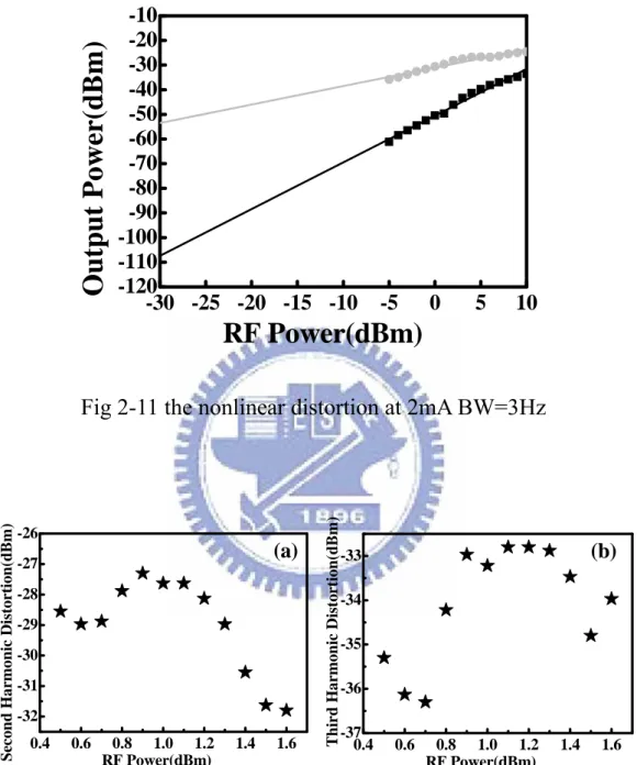
Fig 2-11 the nonlinear distortion at 2mA BW=3Hz………...26
Fig 2-12 (a) the second harmonic distortion (b) the third harmonic distortion at 2mA and resolution is 3kz………..26
Fig 2-13 the nonlinear distortion at different RF power ( BW : 30kHz )…………..27
Fig 2-14 the nonlinear distortion at different modulation frequency (BW:30kHz)...27
Fig 3-1 the structure of 1.3µm QD VCSEL…...44
Fig 3-2 experimental setup for measurement DC characteristic……….……44
Fig 3-3 I-V and L-I curve of the 1.3µm QD VCSEL (No. 15) ……….45
Fig 3-4 Optical spectrum of the device at different current ………...45
Fig 3-5 experiment setup for the RIN measurement ………..…46
Fig 3-7 RIN spectrum for the device with external light injection……….47 Fig 3-8 the optical spectrum of the device with and without light injection……..47 Fig 3-9 stimulation result of the RIN spectrum with external light injection…….48 Fig 3-10 stimulation result of the frequency response with external light
injection………...48 Fig 3-11 Compare the RIN peaks with the resonant frequency with external light injection………...49 Fig 3-12 experiment setup for the locking region measurement……….49 Fig 3-13 linewidth enhancement factor of the device with QD and QW structure at different current………50
Chapter 1 Introduction
1-1 Introduction of Quantum Dot VCSEL
Vertical-cavity surface-emitting lasers (VCSELs) have been researched in recent year. The reduction of the gain length has to compensate by a high Q cavity. There are some advantages of VCSELs, such as low power consumption, circular beam and 2D integrator resulting in important applications in optical fiber communications. Recently, QD structure with some ultra advantages in active layer has been studied [1-3]. The density of state of the QD structure is discrete energy levels, because it is atom-like. Active layer with QD structure has some advantages, such as ultra low threshold current [4-5], higher deferential gain, lower linewidth enhancement factor and insensitive in different temperature. VCSELs at around 1.3µm fabricated on GaAs substrates have been expected to realize high-performance and low-cost light sources for fiber communication systems. The large conduction offset improves the temperature performance over that of conventional InP-based materials.
1-2 Review of Injection locking technique
Injection locking technique has been studied for many years. In 1980 Kobayashi and Kimura used GaAs lasers to demonstrate the injection locking experimental results. [6] Using two devices with close wavelength is necessary. In 2005 Lukas Chrostowski, Xiaoxue Zhao and Connnie J Chang-Hasnain used 1.55µm VCSEL to
demonstrate the resonance frequency enchanced from 7GHz up to ~50GHz [7]. The technique is that one laser the master laser (ML) is external light source to inject photons in another laser the slave laser (SL). The physical reason of the resonant frequency enhancement might result from the external light inject into the slave laser as a cavity increase the photons in the slave laser. .Using the technique has some advantages, such as side-mode suppression, enhancement the relaxation oscillation, improvement nonlinear characteristic and chip, reducing noise. It makes direct modulation more suites for many applications.
For CATV and fiber radio systems, the direct modulation of semiconductor lasers can be used for transmitting subcarrier-multiplexed signals at low cost of using injection locking to improve the nonlinear characteristic.[8] For optical communication, the resonance frequency enhancement by using the injection locking technique means that we will have much larger bandwidth can be used. The technique can greatly improve the operation characteristic give use more freedom to pick device for communication system so that injection-locked direction lasers is a viable way to use for future analog and digital networks.
1-3 Review of Linewidth enhancement factor
In 1981, Fleming and Mooradian demonstrated the linewidth of a semiconductor laser and found the linewidth is different from Schawlow-Townes predicted. They
were unable to explain the result [9]. In 1982, Charles H. Henry wrote a paper about the theory of the linewidth of semiconductor [10]. In general, the phase of the optical field fluctuation to influence the laser linewidth. The fluctuations are due to the spontaneous emission. Linewidth enhancement factor(α) is the deviation of the imaginary part and real part of the refraction index.
'
"
n
n
α
=
∆
∆
The linewidth brooding is attributed to the change in refractive index with carrier density. From the Kramers-Kronig relations, we can find the change in the imaginary part of the susceptibility will change the real part of the susceptibility. A symmetrical gain curve will lead to the dispersion curve of the refractive index has a zero at the frequency corresponding to the gain peak. [11]
Large value of linewidth enhancement factor will result in chirp under direct modulation in optical fiber communication. A symmetric gain spectrum will make linewidth enhancement factor close to zero so that the index of refraction will not change with the carrier density. The quantum dot structure is atom-like. In the theoretically, the density of states of the quantum dot structure is a series of delta-function, its gain spectrum ideally satisfies the criteria.
There are sever methods to measure the linewidth enhancement factor, such as RF-modulation measurement, the interferometric measurement, the amplified
spontaneous emission (ASE) method and using the locking region measurement [12]
1-4 Organization of the Dissertation
This thesis consists of two related parts about two devices respectively. In Chapter 2, we demonstrate 1.3 µm QD VCSELs dynamic properties including DC characteristic, RIN measurement with and without external light injection and linewidth enhancement factor. We also stimulate the RIN spectrum and frequency response. Using the external light injection technique, the device relaxation frequency can be reach to 19.2GHz
In Chapter 3, we report the experimental dynamic characterization of 0.98µm QD VCSEL. We demonstrate DC characteristic, RIN measurement, eye diagram and nonlinear distortion. We also use the calibration method to obtain the intrinsic frequency response of the laser.
Reference
[1] S. L. Chuang, N. Holonyak, Jr. “Quantum-well assisted tunneling injection quantum-dot lasers,” Conference on Lasers and Electro-Optics, Technical Digest, vol. 1, pp. 297, 2002.
[2] T. Yang, J. Tatebayashi, S. Tsukamoto and Y. Arakawa,” Highly uniform self-assembled InAs/GaAs quantum dots emitting at 1.3µm by metalorganic chemical vapor deposition,” Physica E, vol. 26, pp. 77-80, 2005.
[3] N. N. Ledentsov, "Long-wavelength quantum-dot lasers on GaAs substrates: from media to device concepts," IEEE Journal of Selected Topics in Quantum Electronics, vol. 8, pp. 1015 - 1024, 2002.
[4] N. N. Ledentsov, M. Grundmann, F. Heinrichsdor, D. Bimberg, V.M. Ustinov, A. E.Zhukov, M. V. Maximov, Zh. I. Alferov, J. A. Lott, “Quantum-Dot Heterostructure Lasers,” IEEE Journal of Selected Topics in Quantum Electronics, vol. 6, no. 3, pp. 439-451, 2000.
[5] J. A. Lott, N. N. Ledentsov, V. M. Ustinov, A. Yu. Egorov, A. E. Zhukov, P. S. Kop’ev, Zh. I. Alferov, and D. Bimberg, “Vertical cavity lasers based on vertically coupled quantum dots,” Electronics Letters, vol. 33, pp. 1150-1151, 1997.
[6] S. Kobayashi and T. Kimura,"Coherence on injection phase-locked AlGaAs semiconductor laser," Electronics Letters, vol. 16, pp. 668-670, 1980
[7] Lukas Chrostowski, Xiaoxue Zhao and Connie J. Chang-Hasnain, “50 GHz Directly-Modulated Injection-Locked 1.55 µm VCSELs,” Optical Society of America, 2005
[8] Erwin K Lau,"High-Speed Modulation of Optical Injection-Locked Semiconductor Lasers," Electrical Engineering and Computer Sciences University of
California at Berkeley, 2006
(GaA1)As diode lasers,’’ Appl. Phys. Lett., vol. 38, p. 511, 1981.
[10] CHARLES H. HENRY, “Theory of the Linewidth of Semiconductor Lasers,’’
IEEE journal of quantum electronics, vol. QE-18, no. 2, February 1982
[11] MAREK OSINSKI and JENS BUUS, “Linewidth Broadening Factor in semiconductor Lasers-An Overview” Quantum Electronics, IEEE Journal of, 1987 [12] G. Liu, X. Jin, and S. L. Chuang,“Measurement of Linewidth Enhancement Factor of Semiconductor Lasers Using an Injection-Locking Technique” IEEE
Chapter 2 Dynamical characteristics of 0.98
µm QD VCSEL
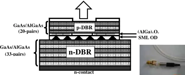
2-1 Sample structure and Fabrication process
The VCSEL structures were grown on GaAs (001) substrates by molecular-beam epitaxy (MBE) method. The bottom DBR structure consists of 33-pairs n-doped GaAs–Al0.9Ga0.1As, the cavity is an undoped Al0.15Ga0.85As and the top DBR consists
of 20-pairs p-doped GaAs–Al0.9Ga0.1As. P-type doping uses Carbon and n-type
doping uses silicon [1]. In order to obtain the output wavelength is 0.98µm, the layer thicknesses and compositions were needed to be designed. To reduce the series resistance, a 10-nm interface region between the GaAs-Al0.9Ga0.1As DBR layers was
modified by linearly composition grading along with relatively high doping. The Al composition profile was achieved by the digital-alloy technique—inserting a monolayer of GaAs after fixed number of monolayer of Al0.9Ga0.1As. The optical
cavity contains the three-stack SML InGaAs QD active region with 8-nm-thick GaAs spacers placed at an antinode of the optical-field intensity. The device structure is shown in Fig.2-1.
2-2 DC Characteristics of QD VCSEL
Fig. 2-2 shows the output power of the device versus current curve (L-I). We measure the device L-I at different temperature. We observer the L-I curve are not smooth due to multi transverse mode occur at higher current operate. Fig. 2-2 also
Eq. 2-3.1
t j pm p pm p p t j m m t j m me
n
n
t
n
n
n
e
n
n
t
n
n
n
e
I
I
t
I
I
I
ω ω ωω
ω
ω
)
(
)
(
)
(
)
(
)
(
)
(
0 0 0 0 0 0+
=
+
=
+
=
+
=
+
=
+
=
shows the voltage of the device versus current curve (I-V).
2-3 Frequency Response
2-3-1 Theory
The rate equations describe the carrier number, the photon number and the phase variation. From the rate equation, we can derive the frequency response of the device and the relaxation resonance frequency.
Consider the application a DC current above the threshold current, I0, carried
with a small AC signal, Im, to the device. The small modulation signal with harmonics
wave and the frequency is ω. Assume Im << I0 bias and spontaneous emission term,
β, is neglected. Small signal can be express as:
The rate equation can be express as:
p p sp p tr p p tr
n
R
n
n
n
g
dt
dn
n
n
n
g
n
qV
I
dt
dn
τ
β
τ
−
+
−
=
−
−
−
=
)
(
)
(
0 0Eq. 2-3.2
For the photon equation: p pm pm m p pm p m pm m m m
n
n
n
g
n
n
g
dt
dn
n
n
g
n
n
g
n
qV
I
dt
dn
τ
τ
−
−
=
−
+
−
=
)
(
)
(
0 0 0 0 0 0 0 0Eq. 2-3.3
Express the rate equations of carrier and photon in frequency domain. For the carrier equation:
)
(
)
(
)
(
)
(
]
1
[
)
(
)
(
)
(
)
(
)
(
)
(
)
(
)
(
)
(
)
(
)
(
)
(
0 0 0 0 0 0 0 0 0 0 0 0ω
ω
ω
τ
ω
ω
ω
τ
ω
ω
ω
ω
ω
ω
τ
ω
ω
ω
ω
ω ω ω ω ω pm m m p m p pm m m m t j m p t j pm t j m t j m t j mn
n
g
qV
I
n
n
g
j
n
n
g
n
n
g
n
qV
I
n
j
e
n
n
g
e
n
n
g
e
n
qV
e
I
e
n
j
+
=
+
−
⇒
−
+
−
=
⇒
−
+
−
=
)
(
)
(
]
1
)
(
[
)
(
)
(
)
(
)
(
)
(
0 0 0 0 0 0ω
ω
τ
ω
τ
ω
ω
ω
ω
ω
m p pm p p pm m p pm pmn
n
g
n
n
g
j
n
n
n
g
n
n
g
n
j
=
+
−
⇒
−
+
=
⇒
We obtain two equations relative to the carrier and photon and then solve the two equations to get the carrier and photon equation at frequency domain.
)
)
(
)(
(
)
(
)
)
(
)(
(
)
(
2 2 2 2 2qV
I
j
n
qV
I
j
j
n
m r r p pm m r mω
ω
ω
ω
ω
τ
ω
ω
ω
ω
ω
ω
ω
−
−
Ω
=
−
−
Ω
=
Eq. 2-3.4
Eq. 2-3.5
0 0 0 0 2 2(
2
f
)
(
n
)
g
;
1
n
g
p p p r r=
π
=
τ
Ω
=
τ
+
ω
When small signal carrier injection in the diode, it induces photon and oscillation. This phenomenon can be observer by measure the frequency response. The natural frequency of oscillation associated with this mutual dependence between carrier and photon. Modulation response is expanded the small signal modulation relationship to steady-state. From Eq. (2-3.4), the modulation response is denoted as
2 2 2 2 2 2 2 2
)
0
(
)
(
)
(
r r r r p r r p pm pmj
j
n
n
H
ω
ω
ω
ω
ω
ω
τ
ω
ω
ω
ω
τ
ω
ω
−
−
Ω
=
−
−
Ω
=
=
Transfers function, H(w), describing the response of the laser intensity at the drive current with small variations through the active region.
γ
π
ω
2
)
(
2 2 2f
j
f
f
f
C
H
r r+
−
=
Eq. 2-3.6
constant C ; factor damping the ; frequency resonance the fr :γ
: :Taking the carrier transport and parasitic elements into account additional extrinsic limitations related to the laser structure results in an extra pole in the small signal modulation transfer function.
)
1
1
(
)
2
(
)
(
2 2 2 p r rf
f
j
f
j
f
f
f
C
H
+
⋅
+
−
=
γ
π
ω
Eq. 2-3.7
The fp is the cutoff frequency due to the parasitic effect, like a low pass filter. For the
application in optical communication system, the device can be operated bandwidth is the most important thing. It is crucial for microwave applications that the modulation bandwidth of the VCSEL is sufficiently large so that efficient modulation is achieved as the modulation frequency.
2-3-2 Experimental Setup
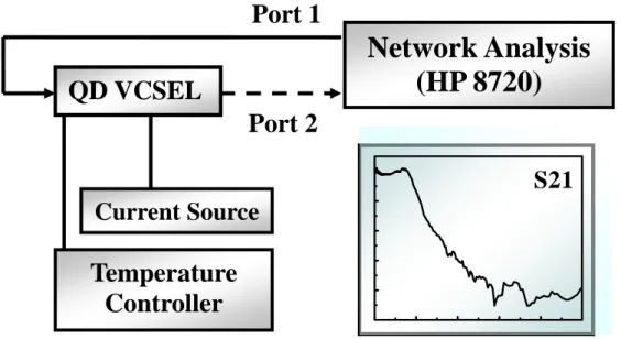
We measure the device response with small signal at different frequency. The microwave test system was mainly consisted of network analyzer, Bias-Tee and high speed photodetector, as illustrated with Fig 2-3. The most important instrument of the microwave measurement is the network analyzer (Agilent 8720ES). Transmitter of network analyzer produced -10dBm RF signal. Current source (Keithley 238) provided direct bias current with the laser diode. Bias-Tee combined AC and DC signal transmission through the coaxial cable. The laser diode was hermetically sealed by a standard TO-Can laser package (TO-46) with a built-in lens. Then, we welded our device on a high speed SMA connector and connected with the coaxial cable.
25-GHz near-IR photodetector (New Focus, model 1414) was received the modulation light signal from the laser diode and was conversed into electrical signal
and fed to network analyzer. Comparing two channels microwave signal by network analyzer, information of transmission and reflection characteristics could be expressed as vector(magnitude and phase), scalar(magnitude only), phase-only quantities, that was, S-parameter.
2-3-3 Frequency Response at different temperature
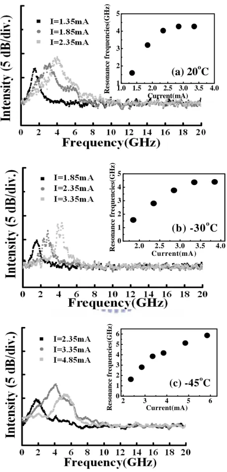
The small signal response of VCSELs as a function of bias current was measured at three different temperature using a calibrated vector network analyzer (Agilent 8720ES). We observer the frequency response increasing with current, but the 3dB will be limited about 2 GHz. Bias at higher current, the frequency response will occur notch phenomenon. The notch phenomenon due to multi-mode operates [2]. We can observer the optical spectrum, will show the multi-mode phenomenon. Fig2-4 shows the frequency response at different temperature and different current.
2-4 RIN measurement
2-4-1 Experimental Setup
We measure the relative intensity noise characteristics of the 0.98µm QD VCSEL. We need to setup a system which can test our sample packaged device and can maintain the device temperature. The Scheme of the measurement system includes current source, temperature controller, and RF spectrum analyzer. Keithley
238 is the current source can provide precisely continuous current to laser diode and measure relative voltage synchronously. The temperature controller model is TED200 with station can maintain the environmental temperature. The RIN spectrum is measured by the RF spectrum analyzer (module Hp 8563E). The resolution of RF spectrum analyzer is 30KHz at experiment result.
2-4-2 RIN measurement at different temperature
The RIN peak is a good indicate the relaxation frequency of the device. We experiment at different current and different temperature. We observer the RIN peak can be reach to higher frequency than the resonant frequency of frequency response observed. Because RIN measurement thought as parasitic free, the RIN peak is not equal to resonant frequency observed from frequency response. It due to the package, external circle will limit the performance of the frequency response. The measurement results show in Fig 2-5. The inset chart is the resonant frequency versus current.
2-5 Frequency Response Calibration
2-5-1 Theory
The frequency response we measure involves the frequency response of the device package. Assume the parasitic components of the laser diode are not power dependent. We subtract the laser frequency response of two different current [3]. By
Eq. 2-5.2
fitting the data, we will get the intrinsic parameter. The measure data:
2 2 1 2 2 1 2 4 1 2 2
)
2
(
)
(
).
(
)
(
f
f
f
f
f
H
f
H
r r r parasitic free⋅
⋅
+
−
=
π
γ
Eq. 2-5.1
Subtract the data of two different current:
)
)
2
(
)
(
)
2
(
)
(
(
log
10
)
(
4 2 2 2 2 2 2 2 2 2 2 1 2 2 1 2 4 1 10 r r r r r rf
f
f
f
f
f
f
f
f
H
⋅
⋅
+
−
⋅
⋅
⋅
+
−
=
π
γ
π
γ
We can observer the parasitic term be eliminated.
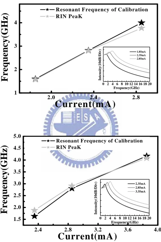
2-5-2 Results and Discussion
We used above method to calibrate the measurement results. By fitting the data
got from the substrate two frequency responses at different current at the same
temperature, we can get the resonant frequency and compare with the RIN peaks.
Fig 2-6 shows the compare results and the stimulation results.
2-6 Eye diagram
Eye diagram can measure the optical time domain to characterize system pulse
and extinction ratio. Eye diagrams are formed by overlaying multiple single-value pseudo-random binary sequence (PRBS) waveforms. The experimental result show on a high speed oscilloscope or eye diagram analyzer.
2-6-1 Experimental Setup
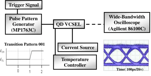
We measure the eye diagram of the 0.98µm QD VCSEL. We need to setup a system which can test our sample. The system includes a trigger signal, Pulse pattern generator (MP1763C), temperature controller, current source and wide-bandwidth oscilloscope (Agilient 86100C). The experiment measurement system shows in Figure 2-7.
2-6-2 Results and Discussion
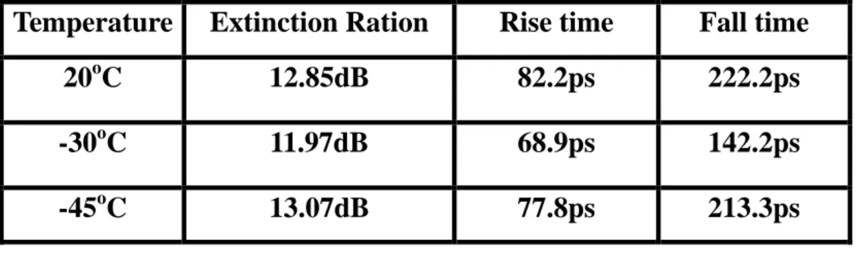
We illustrate the eye diagram at 2.5Gb/s as shown in Fig 2-8. We observer the eye diagram open and list the parameter got from the eye measurement result. From the extinction ration value, the 0.98µm QD VCSEL can be used in 2.5Gb/s system. Extinction ration is the ratio of the maximum value and minimum value. In general, the value should be 6dB.Using the value, we justify the device can be used in system.
2-7 Nonlinear characteristic measurement
2-7-1 Theory
In optical communication system, we wish the transmission signal is accurate the same as origin signal. However, neither device is perfectly linear, particularly when large modulation levels are involved. Several different types of distortion products are common from these components such as harmonic distortion and inter-modulation distortion. Inter-modulation due to the nonlinear effects may distinct two sources. The first is about the rate equation intrinsic nonlinearities cause by the mixing of photons and electrons in the laser cavity. The second is the nonlinearity of the laser power-current curve [4-5].
The intensity modulated is the laser output power with modulated signal at the modulating frequency. It depends on the linearity of the device and there will also be some modulating power at harmonics of the modulating frequency. It is usually some modulated power at the second harmonic and third harmonic of the modulating frequency. Harmonic distortion is defined as the ratio of modulated power in harmonic of the modulating frequency to the power at the modulating frequency.
)
(
)
(
...
)
3
(
)
2
(
)
(
)
3
(
)
(
)
2
(
mod mod mod mod mod mod 3 mod mod 2f
P
nf
P
f
P
f
P
THD
f
P
f
P
HD
f
P
f
P
HD
+
+
+
=
=
=
Eq. 2-7.1
The HD2 is the second harmonic distortion, HD3 is the third harmonic distortion,
and THD is the total harmonic distortion
Two closely spaced signals of intermodulation distortion is third-order intermodulation (IMD). This is because the IMD signals fall close to the original modulating frequencies.
)
(
)
2
(
)
2
(
i j i j if
P
f
f
P
f
f
IMD
−
=
−
Eq. 2-7.2
2-7-2 Experimental SetupWe measure the nonlinear distortion characteristics of the 0.98µm QD VCSEL. We need to setup a system which can test our sample packaged device, signal generator and can maintain the device temperature. The Scheme of the measurement system, illustrates in Figure 2-10, include current source, temperature controller, and RF spectrum analyzer. The signal generator is hp 8657B can generate 0.1~2060 MHz. Keithley 238 is the current source can provide precisely continuous current to laser
diode and measure relative voltage synchronously. The temperature controller model is TED200 with station can maintain the environmental temperature. The nonlinear distortion characteristic is measured by the RF spectrum analyzer (module Hp 8563E). The resolution of RF spectrum analyzer is lMHz at experiment result.
2-7-3 Results and Discussion
We measure nonlinear characteristic at different RF power at 1GHz and the device bias at 2mA. The experimental result shows in Fig 2-11. From the figure we can obtain SFDR is about 76dB. We also measured the second and third harmonic distortion at different RF power. Finally, we show the nonlinear characteristic at two different conditions. Fig 2-13 shows the device at different RF power. Fig 2-14 shows the device at different modulation frequency.
2-8 Summary
We report the dynamic characteristics of the 0.98µm QD VCSEL. We also present the device structure about 0.98µm QD VCSEL、the L-I&I-V curves、the RIN measurement at different temperature、frequency response calibration method、the eye diagram at different temperature and the nonlinear distortion. The RIN peak is the relaxation frequency. We also use the calibration method to find the device frequency response. A 2.5 Gb/s non-return-to-zero (NRZ) pseudo-random binary sequence (PRBS) data with 231-1 pattern length from a pattern generator used to directly modulate the QD VCSEL. The eye diagrams can be clearly observed. We also measure the nonlinear distortion at different modulation frequency and at different modulation power.
Reference
[1] Sergey A. Blokhin, Nikolai A. Maleev, Alexander G. Kuzmenkov, Alexey V. Sakharov, Marina M. Kulagina, Yuri M. Shernyakov, Innokenty I. Novikov, Mikhail V. Maximov, Victor M. Ustinov, Alexey R. Kovsh, Sergey S. Mikhrin, Nikolai N. Ledentsov, Gray Lin, and Jim Y. Chi, “Vertical-Cavity Surface-Emitting Lasers Based on Submonolayer InGaAs Quantum Dots, “IEEE journal of quantum
electronics, VOL. 42, 2006
[2] Yinon Satuby and Meir Orenstein, “Small-Signal Modulation of Multitransverse Modes Vertical-Cavity Surface-Emitting Semiconductor Lasers, “IEEE photonics
technology letters, VOL. 10, 1998
[3] P. A. Morton, T. Tanbun-Ek, R. A. Logan, A. M. Sergent, P. F. Sciortino, Jr., and D. L. Coblentz, “Frequency Response Subtraction for Simple Measurement of Intrinsic Laser Dynamic Properties, “Photonics Technology Letters, IEEE,1992
[4] Anders Larsson, Christina Carlsson, Johan Gustavsson, Åsa Haglund, Peter Modh and Jörgen Bengtsson, “Direct high-frequency modulation of VCSELs and applications in fibre optic RF and microwave links, “New J. Phys. 6,2004
[5] ROBERT OLSHANSKY, VINCENT A. LANZISERA, AND PAUL M. HILL, “Subcarrier Multiplexed Lightwave Systems for Broad-Band Distribution, “journal of
Fig 2-2 I-V and L-I curve of the 0.98µm QD VCSEL at different
GaAs/AlGaAs
Fig 2-1 The structure of the 0.98 µm VCSEL with SML QD
temperature
n-contact GaAs/AlGaAs (33-pairs) SML QD (20-pairs) (AlGa)xOyn-DBR
p-DBR 0 2 4 6 8 10 12 0 1 2 3 4 5 6 7 8 20oC I-V L-I Current(mA) Voltage(V) 0.0 0.1 0.2 0.3 0.4 0.5 Power (mW) 0 2 4 6 8 10 12 0 1 2 3 4 5 6 7 8 I-V L-I Current(mA) Vo lt ag e(V) 0.0 0.1 0.2 0.3 0.4 0.5 -30oC Power (mW) 0 2 4 6 8 10 12 14 16 0 1 2 3 4 5 6 7 I-V L-I Current(mA) Voltage(V ) 0.0 0.1 0.2 0.3 0.4 0.5 -45oC Power (mW)Fig 2-3 experimental setup for measurement frequency response
Fig 2-4 frequency response of the device at different temperature
Temperature
Controller
Current Source
Port 1
Network Analysis
(HP 8720)
QD VCSEL
Port 2
S21
0 2 4 6 8 10 -50 -40 -30 -20 -10 0 In tensity(dB) Frequency(GHz) I=1.85mA I=2.35mA I=3.35mA 0 2 4 6 8 10 -50 -40 -30 -20 -10 0 (-30oC) Intens ity(dB) Frequency(GHz) I=1.85mA I=2.35mA I=3.35mA 0 2 4 6 8 10 -50 -40 -30 -20 -10 0 (-45oC) Intens ity(dB) Frequency(GHz) I=2.35mA I=2.85mA I=3.35mA1.0 1.5 2.0 2.5 3.0 3.5 4.0 1 2 3 4 5
(a) 20
oC
R eso na n ce fr eq ue nc ie s( GHz ) Current(mA) 2.0 2.5 3.0 3.5 4.0 0 1 2 3 4 5(b) -30
oC
Res o n a nce frequencies (GHz) Current(mA) 2 3 4 5 6 0 1 2 3 4 5 6(c) -45
oC
Resonan ce freq uenci es(GHz) Current(mA)2.0 2.4 2.8 1 2 3 4
Frequency(GHz)
C urrent(m A)
Resonant Frequency of Calibration RIN PeaK 0 2 4 6 8 10 12 14 16 18 20 Intens ity (10dB/ Div) Frequency(GHz) 1.85mA 2.35mA 2.85mA 2.4 2.8 3.2 3.6 4.0 1.5 2.0 2.5 3.0 3.5 4.0 4.5 5.0
Frequen
cy(GHz)
Current(mA)
Resonant Frequency of Calibration RIN PeaK 0 2 4 6 8 10 12 14 16 18 20 Intensity( 10dB /Div) Frequency(GHz) 2.35mA 2.85mA 3.35mA
Fig 2-7 experimental se
surement eye
Fig 2-8 the eye diagram of the device with 2.5 Gb/s
Trigger Signal
tup for mea
diagram
Temperature
Controller
Current Source
QD VCSEL
Wide-Bandwidth
Oscilloscope
Pulse Pattern
(Agilient 86100C)
Time( 100ps/Div)Transition Pattern 001
Generator
Time (100 ps / div.)
2.5 Gb/s
Temperature
E
xtinction Ration
Rise time
Fall time
82.2ps
11.97dB
68.9ps
C 13.07dB
Fig 2-9 the parameter obtain from
20
oC 12.85dB
222.2ps
-30
oC
142.2ps
-45
o77.8ps
213.3ps
eye diagram
Fig 2-10
experimental setup for measurement nonlinear d
istortion
0 1 2 3 4 5 -70 -60 -50 -40 -30 -20 In te n s ncy(GHz ity (dB) Freque )
Tem
Contro
perature
ller
Current Source
QD VCSEL
RF Spectrum
analyzer
RF signal
Port 1
Port 2
-30 -25 -20 -15 -10
-5
0
5
10
-120
-110
-100
-90
-80
-70
-50
-40
-30
-20
-10
-60
Output Power(dBm)
RF Power(dBm)
Fig 2-11 the nonlinear distortion at 2mA BW=3Hz
Fig 2-12 (a) the second harmonic distortion (b) the third harmonic
distortion at 2mA and resolution is 3kz
0.4 0.6 0.8 1.0 1.2 1.4 1.6 -32 -31 -30 -29 -28 -27 -26 (a) Se co nd Har m oni c Disto rt io n (dB m ) RF Power(dBm) 0.4 0.6 0.8 1.0 1.2 1.4 1.6 -37 -36 -35 -34 -33 (b) Th ir d H a rmon ic D is torti on (dBm) RF Power(dBm)
Fig 2-13 t
30kHz )
rent modulation frequency
: 30kHz )
0.0 0.5 1.0 1.5 2.0 2.5 3.0 3.5
he nonlinear distortion at different RF power ( BW :
-80 -70 -60 -50 -40 -30 -20 -10 0 In tens ity(dBm) Frequency(GHz) RF Frequency=1GHz RF Power=0dBm 0.0 0.5 1.0 1.5 2.0 2.5 3.0 3.5 -80 -70 -60 -50 -40 -30 -20 -10 0 In tens ity(dBm) Frequency(GHz) RF Frequency=1GHz RF Power=10dBm 0.0 0.5 1.0 1.5 2.0 2.5 3.0 3.5 -80 -70 -60 -50 -40 -30 -20 -10 0 In tensity(dBm) Frequency(GHz) RF Frequency=1GHz RF Power=10dBm 0.0 0.5 1.0 1.5 2.0 2.5 3.0 3.5 -80 -70 -60 -50 -40 -30 -20 -10 0 In tensity(dBm) Frequency(GHz) RF Frequency=0.8GHz RF Power=10dBm
Fig 2-14 the nonlinear distortion at diffe
( BW
hapter 3 Dynamical characteristics of 1.3
µ
m QD VCSEL
-A
cture to achieve some excellent characteristic. The ss of the cavity active region is 3λ. Carbon was used as the p-type dopant in the DBR to increase the carrier concentration (2-3×1018 cm-3). In order to reduce the series resistance, the interfaces of both the p-type and n-type Al0.9Ga0.1As/GaAs DBR
layers are linearly graded. The optical characteristics of QDs were optimized through PL measurement and structural analysis. The details of the process were fully described in our previous works [1]. The mesa diameter of the device is 26µm with a
re, and the device surface is quasi-planar so that the annular me level. The device structure is shown The p-contact was formed by directly depositing Ti/Pt/Au on the upper
ed p+ GaAs contact layer, and Au/Ge/Ni/Au was deposited on the bottom side of the substrate after it had been thinned down, and the shaded region beneath the
C
3-1 Sample structure and Fabrication process
The structures were grown on GaAs (100) substrates by using molecular beam epitaxy (MBE) method. The n+ GaAs as buffer layer, The top distributed Bragg reflector (DBR ) is 33.5 pair n+ Al0.9Ga0.1As/n+ GaAs (Si-doped), undoped active
region, p- Al0.98Ga0.02As oxidation layer, The top bottom DBR is 22 pair p+
l0.9Ga0.1As/p+-GaAs and p+-GaAs (carbon-doped) is contact layer. The active
region consisted of QDs stru thickne
5 µm oxide apertu
p-contact metal and the bond pad are on the sa in Fig.3-1.
bond pad represents the implanted region.
3-2 DC Characteristics of QD VCSEL
3-2-1 Experimental Setup
We measure the DC characteristics of the 1.3 µm QD VCSEL such as L-I curve, I-V curve and optical spectrum. We need to setup a system which can test our sample on wafer level or packaged device. Probe station was a basic instrument to meet our needs. Scheme of probe station system, illustrated in Figure 3-2, include probe station, current source, and powermeter module. Keithley 238 is the current source can provide precisely continuous current to laser diode and measure relative voltage synchronously. Newport power meter module (model 1835C) with photodiode and powermeter can be used to measure the light output power of the laser diode by using an integration sphere or measuring directly. The integration sphere is used to pick up part of whole emitting power from VCSEL to improve the accuracy of power measurement. The VCSEL device was placed on a platform of the probe station and was injected bias current with microprobe. From the L-I curve and I-V curve we can get some useful information such as the threshold current, slope efficiency, turn-on voltage and differential resistance. Near-field pattern was obtained by specific CCD. The optical spectrum of the device was measured by optical spectrum analyzer (OSA, Advantest Q8381). The emission light of the device is via optical fiber was package to
optical spectra analyzer. The OSA had spectrum resolution of 0.1nm which was adeq t
ion
3-3 RIN measurement
uate o measure VCSEL lasing spectra.
3-2-2 Results and Discuss
Fig. 3-3 shows the output power of the device versus current curve (L-I) and the voltage of the device versus current curve (I-V). The threshold current is ~ 1.1 mA. The output power rollover occurs as the current increases above 4.2mA with maximum optical output of 0.118mW at 20°C. To investigate the wavelength and current relation of the QD VCSEL, optical spectrum curves were measured from 1.5Ith to 3Ith with step of 0.5Ith. Fig 3-4 shows the result of the optical spectrum at
different current. We can observer the optical spectrum with single transverse mode operation in the whole operation range with a lasing wavelength about 1.278µm.
3-3-1 Theory
The RIN peak is a good indicate of the relaxation frequency of the device. The deriving force not input current is the Langevin force (Fs, Fn and Fφ) of the field due
to the spontaneous emission. The Langevin force is assumed to be uncorrelated white Gaussian noise [3]. The relative intensity noise (RIN) spectrum is frequency
The intrinsic relative intensity noise of a device is defined as 2
)
(t
P
RIN
=
<
δ
2>
0P
Eq. 3-3.1
P0 is the mean square power fluctuation. From a
smal
average power and δP(t)2 is the
l-signal analysis of the rate equations for a single-mode laser, we can derive the noise spectrum of the device. The relative intensity noise spectrum of external light injected locked device can be derived using the follow rate equations [2].
th s inj s sp inj inj c th
N
N
G
N
I
dN
F
t
S
k
f
N
N
G
d
F
R
t
S
S
k
S
S
N
N
G
dS
−
+
−
⋅
−
∆
⋅
−
−
⋅
=
+
+
−
⋅
⋅
+
−
⋅
−
=
φ
φ
π
α
φ
φ
φ
)
(
)
)
(
cos(
2
)
(
0 0 n inj c th pF
S
S
q
dt
S
dt
S
dt
+
⋅
+
−
−
=
+
ε
τ
τ
ε
φ1
)
)
(
sin(
2
)
(
2
1
0Eq. 3-3.2
S ,φ and are the photon number, the phase and the carrier number inside the slave laser cavity. is the gain coefficient, is the transparency carrier number,
N
0
G N0
p
τ i I is the slave laser bias current, ε
α is the linewidth enhancement factor.
and are th s.
s
F ,Fφ Fn e noise term ∆ is the detuning between the master and slave ω
laser. is the photons injection into the slave laser. is the coupling coefficient, which determined by the photon injected into the cavity-round trip time. We use the injection-locked rate equation to simulation the experimental results.
We used the RIN measurement to find the device relaxation frequency with the
inj
S kc
s the photon lifetime, τnis the carrier lifetime, is the gain compression factor, and
exter e slave laser and depletes the carrier density. It makes the spontaneous emission rate reduced and more photons are coupled in phase into the amplified injection field. The more photons in phase and the relaxation frequency should enhance. The RIN spectrum represent the relaxation frequency peak becomes higher with injections. At a lower injection level directly adds photons into the slave laser cavity by using more carriers, which compensates the gain saturation and enhances the relaxation peaks of the slave laser. At stronger injections, the injected photons deplete the most of the available carriers, eventually saturate the signal and decrease the relaxation peaks. It preve
improvement of the relaxation frequency.
3-3-2 Experimental Setup
We measure the relative intensity noise characteristics of the 1.3 µm QD VCSEL. We need to setup a system which can test our sample packaged device and can maintain the device temperature. The Scheme of the measurement system, illustrates in Figure 3-5, include current source, temperature controller, semiconductor optical amplifier (SOA), and RF spectrum analyzer. Keithley 238 is the current source can provide precisely continuous current to laser diode and measure relative voltage synchronously. The temperature controller model is TED200 with station can
nal light injection. The light injected into the cavity of th
spectrum analyzer (module Hp 8563E). The resolution of RF spectrum analyzer is lMHz at experiment result. The external light source is tunable laser.The polarization of the tunable laser is adjusted using a polarization controller before injecting into the QD VCSEL.
3-3-3 Without light injection
Form the RIN spectrum without light inject, we can observe the RIN peak will shift to higher when the bias current higher. At 2.2Ith we can find the RIN peak move to 1.83GHz. The frequency at RIN peak is close to the resonant frequency can be found form frequency response. Fig3-6 shows the device without light injection experiment result.
3-3-4 With light injection
Using the injection locking technique, we can enhance the bandwidth of the device. From the frequency response, we observer the bandwidth improve better when increasing the injection power and the bandwidth increase form 1.75GHz to 7.11GHz. The bandwidth will be limited by the package and external circuit. The RIN measurement is capacitance free. The RIN peak is a good indicate the relaxation frequency of the device. We experiment the external light injection at different current and different injection power. We observer the RIN peak can be reach to 19.2GHz at
bias 1.3mA, wavelength detune 0.081nm and external light power 3dBm. From the optical spectrum, we can observer when the light inject into the QD VCSEL. The external photons in the cavity of the device will compete deplete the gain and replace the origin wavelength of the device. Fig3-7 shows the device with light injection RIN measurem optical spectrum with and without light injection.
3-4 Simulations
ed to tion between photons and carriers inside a laser cavity. When an additional light source is injected into the cavity, the system preserves the general form of the original equations, but with extra terms describing the effects of the injection.
ent result. Fig3-8 shows the device
3-4-1 Theory
We based model of injection-locked rate equation (Eq 3-3.2) is usually us describe the interac
0 1 0 1 0 1
( )
,
( )
,
( )
( )
,
( )
,
( )
j t j t j t s s N N j t j t j t φ φF
F
e
F
F
e
F
F
e
S
S
S
e
e
N
N
N
e
ω ω ω ω ω ωFor the photon part:
ω
ω
ω
ω
φ φ φ ω
ω
=
=
=
=
+
=
+
=
+
0 0 0 0 1 1 0 0 0 1 0
(
)
( )
( )
( )
( )(1
)
2
1 1 0 0 0 0 11
1
1
( )
2 (
cos(
)
sin(
) ( ))
( )
j t trc inj inj inj s
G N
N
S
G N
S
e
i S
S
S
S
p injS
S
S
S
S
k
S S
F
ωε
ω
ω
ω ω
=
−
ω
−
+
−
Eq. 3-4.1
1( )
i
k
ε
ε
ε
τ
ω
φ φ
φ φ φ ω
ω
+
+
+
+
−
−
−
+
For the phase part:
0 1 1 0 0 1 0
( )
( )
(
(
sin(
) cos(
) ( ))
( )
2
2
inj c inj injS
G N
S
F
S
φα
ω
ω
ωφ ω
=
−
−
φ φ
−
+
φ φ φ ω
−
+
ω
Eq. 3-4.2
Finally, for the carrier part:
0 0 0 0 1 1 1 1 0 0 0
(
)
( )
0( )
( )(1
)
( )
1
1
1
t tr n sG N
N
S
G N
i N
S
S
F
S
S
S
ωε
ω
( )
jN
ω
e
ω ω
ω
ω
τ
ε
ε
ε
−
= −
−
−
−
+
+
+
+
Eq. 3-4.3
Equations (2-4.1), (2-4.2), (2-4.3) are written in matrix form: 1 1 s N
S
F
N
F
i
ω
⎡ ⎤ ⎡ ⎤
⎢ ⎥ ⎢ ⎥
⎢ ⎥ ⎢ ⎥
⎣ ⎦ ⎣ ⎦
−
⎡
⎤
⎢
1 0 0 0 0 0 0 0 0 0 0 0 0 0 0 0 3 0 0(
)
(1
)
1
1
2
sin(
)
1
1
cos(
)
sin(
)
cos(
)
2
2
(
)
tr c inj inj inj c inj p inj inj c inj c injA
F
G N N
S
S
S
G
k S S
S
S
S
k
S
S
S
k
A
i
k
G
S
S
G N N
S
φφ
ε
ε
ε
φ φ
ε
φ φ
τ
α
φ φ
ω
φ φ
ε
=
⎢ ⎥ ⎢ ⎥
−
−
+
+
−
−
+
+ −
−
=
−
−
+
−
−
−
0 0 0 0 0(1
)
1
1
trS
S
ε
−
ε
+
+
0
⎢
⎢
⎥
0 0 01
1
sG
i
S
S
ω
ε
τ
⎥
⎢
⎥
⎢
⎥
⎢
⎥
⎢
⎥
⎢
⎥
⎢
⎥
⎢
⎥
⎢
⎥
⎢
⎥
+
+ ⎥
+
⎥
⎢
⎥
⎣
⎦
⎢
⎢
⎥
The laser RIN
1
( ) | ( ) |
RIN
ω
=
S
ω
The small-signal modulation response can also be found from this system by considering I as the small signal modulation current.
1 1 1 1
0
0
S
A
N
I
φ
−⎡ ⎤
⎡ ⎤
⎢ ⎥
=
⎢ ⎥
⎢ ⎥
⎢ ⎥
⎢ ⎥
⎢ ⎥
⎣ ⎦
⎣ ⎦
The modulation response transfer function will be
1
| ( )
( )
( )
S
H
I
|
ω
ω
ω
=
3-4-2 RIN simulationFrom the injection locking rate equation, we can stimulate the RIN spectrum of the device at external light injection. The drive force is Langevin force white Gaussian noise with variance is zero. From the stimulation result, we find the higher external light strength and the higher frequency of RIN peaks. It is more photons in phase, when light strength increase. The more photons in the amplifier field increase the relaxation frequency. Fig3-9 shows the RIN spectrum stimulation result.
3-4-3 Frequency Response simulation
current variation. Fig3-10 shows the frequency response stimulation result. The inset chart is the resonant frequency versus the injection power.
Finally, we compare the RIN spectrum and the frequency response stimulation results at the same external light. We can observer the RIN peak is approach to the resonant frequency. The parameter, we stimulate need were listed Fig 3-11. Fig 3-12 e chart. We can observer the RIN peaks and resonant frequency.
3-5 Linew ent factor
nsity [4]. It can be defined as:
3-4-4 Results and Discussion
shows the RIN spectrum and frequency response at the sam
idth enhancem
3-5-1 Theory
In general, the width of a laser output is dependent of the fluctuations in the phase of the optical field. The fluctuations are due to the spontaneous emission alter the phase and intensity of the output field. Linewidth enhancement factor is ratio of the deviation of the imaginary part of the refractive index will change by the carrier density and the real part of the refractive index will change by the carrier de
'/
"/
dn dn
Eq. 3-5.1
dn dn
2
The value o or is dependent on the dimension of the quantization. The complex refractive index changes by the carrier density. We can observer from the follower formulas [5].
The refractive:
'
"
n n
= −
jn
f the linewidth enhancement fact
2 2
2
ε
on
ch(
E
ch−
h
ω
)
+
( / )
h
τ
in ch Eq. 3-5.2 2"( )
1
n
g
R
2 24
(
) /
2
(
)
( /
)
ch c v in ch ch o ch ing
f
f
dE
n
E
λ
ω
=
=
∑ ∫
<
>
(
)(
)
1
'( )
g f
ch cf E
v chn
ω
=
∑∫
<
R
>
−
−
h
ω
dE
π
τ
ε
ω
τ
−
−
h
+
h
h
Eq. 3-5.3The change of the linewidth enhancement factor with different quantization
dimension alters the term of gch. gch is the density-of-states of the electron-hole pair. It
is ex
We use the locking region to calculate the value of the linewidth enhancement
factor. The light of master laser injected into the slave laser at near the output presses by the step and delta functions, for a quantum well and quantum box. The
change in the imaginary part of the susceptibility (gain or loss) will be influence by a
corresponding change in its real part (refractive index) through the Kramers-Kronig
relations. A symmetrical gain curve will lead to a dispersion curve of the refractive
index. It make linewidth enhancement factor is zero at the frequency corresponding to
he slave laser. The formula can be derived form the photon and the phase rate equation.
wavelength of t
)]
/τ
(G
α
θ
)
P
P
L
n
c
dt
dθ
P
θ]
)
P
(
c
/τ
[G
dP
g o mo / i g2
cos
1
+
1 2⋅
⋅
−
=
(
ω
[ω
P
L
n
dt
p / i p1
2
sin
2 1⋅
+
−
+
−
=
Eq. 3-5.4
P is the total photon number and ψis the phase. G is the optical gain and N is the
carrier density. τp is the photon lifetime and ng is the group index. The expression of
the locking bandwidth is given as a function:
)
cos
sin
2
2 1(
θ-α
θ
)
P
P
(
L
n
c
∆ω
i / g⋅
⋅
=
Eq. 3-5.5
When injection locked stable, we can drive the locking bandwidth formula.
2 1 2
1
/ i)
(
=
<
∆
<
+
−
ρ
ρ
ω
α
ρ
We measure the locking region of the 1.3 um QD VCSEL and QW VCSEL. We
need to setup a system which can test our sample packaged device and can maintain
the device temperature. The Scheme of the measurement system, illustrates in
2
gP
P
L
n
c
Eq. 3-5.6
At the same injection power, the ratio of the positive and negative detune. We can
calculate the value of linewidth enhancement factor.
Fig 3-13, include current source, temperature controller, polarization controller, variable attenuator, optical spectrum analyzer (OSA, Advantest 8381), semiconductor optical amplifier (SOA), and wavelength meter. Keithley 238 is the current source can provide precisely continuous current to laser diode and measure relative voltage synchronously. The temperature controller model is TED200 with station can
we need more accurate resolution in our experiment. The resoluation of wavelength meter can reach to 0.001nm. The external light source is tunable laser and can be accurate operated. The polarization of the tunable laser is adjusted using a polarization controller before injecting into the QD VCSEL. We also use a variable attenuator to controller the light power before inject into the polarization controller. We justify the lock or unlocked by the wavelength
ser will become one wavelength observer by the wavelen e use the method to find out the positive and the negative detune at the same external light injection.
maintain the environmental temperature. The optical spectrum analyzer is used to observer the master laser light inject into the slaver laser situation. The max resolution of the optical spectrum analyzer is 0.1nm, but
meter. We can observer the light from master laser complete with slave laser origin output light. Finally, the output light via the slave la
gth m ter. We

![TraditionalMLCalgorithmsmainlytacklethebatchMLCproblem,wheretheinputdataarepresentedinabatch[24,28].Nevertheless,inmanyMLCapplicationssuchase-mailcategorization[22],multi-labelexamplesarriveasastream.Onlineanalysisistherefore dimensionreducermotivatedbyma](data:image/gif;base64,R0lGODlhAQABAIAAAP///wAAACH5BAEAAAAALAAAAAABAAEAAAICRAEAOw==)