This content has been downloaded from IOPscience. Please scroll down to see the full text.
Download details:
IP Address: 140.113.38.11
This content was downloaded on 28/04/2014 at 08:43
Please note that terms and conditions apply.
Capacitance Dispersion in n-LT-i-p GaAs Structures with the Low-Temperature Layers
Grown at Different Temperatures
View the table of contents for this issue, or go to the journal homepage for more 1999 Jpn. J. Appl. Phys. 38 L1425
(http://iopscience.iop.org/1347-4065/38/12A/L1425)
Jpn. J. Appl. Phys. Vol. 38 (1999) pp.L1425–L1427 Part 2, No. 12A, 1 December 1999
c
°1999 Publication Board, Japanese Journal of Applied Physics
Capacitance Dispersion in n-LT-i-p GaAs Structures with the
Low-Temperature Layers Grown at Different Temperatures
Jenn-Fang CHEN, Nie-Chuan CHEN, Pai-Yong WANG, Jiin-Shung WANGand Chi-Ming WENG
Department of Electrophysics, National Chiao Tung University, Hsinchu, Taiwan, R.O.C.
(Received September 16, 1999; accepted for publication October 13, 1999)
The electrical properties of annealed low-temperature GaAs are studied by investigating the frequency-dependent capaci-tance of n-LT-i-p structures with the low-temperature (LT) layers grown at different temperatures. Relative to the sample grown at 610◦C, the samples grown at 200, 300 and 400◦C show significant capacitance dispersions over frequency which is explained by the emission of carriers from traps. Based on a proposed band diagram where a dominating trap at 0.66–0.74 eV exists in the LT layers, the high-frequency dispersion is shown to be affected by resistance-capacitance (RC) time constant effects. From the mid-frequency capacitance versus voltage characteristics, the concentrations of the occupied traps are estimated to be
≈1017cm−3for samples grown at 200, 300 and 400◦C, which are found to be consistent with those obtained from analyzing
the current-voltage characteristics of n+-LT-n+structures.
KEYWORDS: low-temperature GaAs, deep levels, capacitance-frequency spectra
L1425
Recently, there has been considerable interest in under-standing the underlying mechanisms1, 2)for the large resistiv-ity and short carrier lifetime in low-temperature (LT) grown GaAs. A large concentration of defects such as AsGa
anti-sites3, 4)or various complexes5)or arsenic precipitates2)acting
as buried Schottky barriers have been proposed. Despite these studies, the relative roles of different defects in rendering the LT GaAs high-resitivity and short lifetime still remains under contention. In our previous studies6)on LT GaAs, dc
resistiv-ity measurements revealed the existence of a dominating trap at 0.66 eV below the conduction band, which is related to the semi-insulating property. In this work, we continue this study by carrying out the ac measurement on the electrical proper-ties of LT GaAs grown at different temperatures.
The samples studied here are p-i-n GaAs diodes with part of the intrinsic layer grown at different temperatures. All sam-ples were grown by a Varian Gen-II molecular beam epitaxy (MBE) system on n+-(001) GaAs substrates. The structure of the samples consists of 0.2µm n(5 × 1017cm−3)/0.2µm undoped-layer grown at 200, 300, 400, and 600◦C, respec-tively/0.6µm intrinsic layer/0.4 µm p(1×1017cm−3)/0.5µm
p+(>1018cm−3). Besides the 0.2µm undoped-layer, all the
remaining layers were grown at 610◦C. Details of the growth have been reported previously.6)Figure 1 shows the
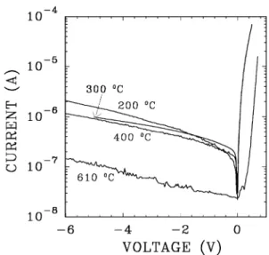
current-voltage (I –V ) characteristics at 376 K for the samples. All four samples show typical rectified I –V curves. The diame-ter of both diodes is 500µm. It can be seen that the samples grown at 200, 300 and 400◦C have similar reverse-bias cur-rents which are higher compared to that of the sample grown at 600◦C, indicating that the leakage current is increased by the existence of defects introduced by the LT growth.
Figure 2 shows the capacitance-frequency (C-F) spectra at a bias of −2 V for all the samples. Relative to the sam-ple grown at 610◦C, the samples grown at 200, 300 and 400◦C show similar C-F spectra with two step-like capac-itance dispersions over frequency. The low-frequency dis-persion, where capacitance drops from ≈120 pF to ≈40 pF, was previously identified to be the holes emitted from traps near the midgap.7)Here, we are mainly interested in the
high-frequency dispersion where capacitance drops from≈40 pF to≈30 pF. According to the theory of admittance spectrso-copy, the inverse of the frequency at which the capacitance drops corresponds to the emission time of carriers from traps,
Fig. 1. The I –V characteristics at 376 K for the samples grown at 200, 300, 400 and 610◦C.
pacitance reduces to Ch = C1C2/(C1+ C2) = 30 pF which
is equal to the experimental high-frequency capacitance as shown in Fig. 2 for samples grown at 200, 300 and 400◦C.
When the signal frequency is sufficiently low, the electrons where R and C1 = Aε/d = 120 pF represent the
resistiv-ity and geometric capacitance of the highly-resistive LT layer (0.2µm) and C2 = 40 pF is the geometric depletion
capac-itance for the intrinsic layer (0.6µm). At high frequencies where 1/ω ¿ (C1+C2)R, only the free carriers on both edges
of n and p regions can be modulated, the high-frequency ca-from modified emission timeτ T2 versus 1000/T , the
acti-vation energies (capture cross sections) were obtained to be 0.66 eV (1.1 × 10⁻¹¹cm2), 0.66 eV (5.6 × 10⁻¹¹cm2) and
0.74 eV (1.5 × 10⁻¹⁰cm2) for the samples grown at 200, 300
and 400◦C, respectively.
To show that this capacitance dispersion is affected by the large resistivity due to the LT growth, let us refer to a simpli-fied band diagram and its equivalent circuit in Fig. 3, where an acceptor trap is assumed in the LT layer. Analysis of the equivalent circuit yields the capacitance:
C(ω) = C1C2 C1+ C2 · 1+ C2/C1 1+ ω2R2(C 1+ C2)2 ¸
are emitted from traps at the edge of the LT layer with an emission time constant τt and traverse through the
highly-resistive LT layer with a time constantτRC = R(C1+ C2).
Because the large R for the LT layer, let us assume that
R(C1+ C2) > τt, therefore, the capacitance drops at the
in-flexion frequencyω = τ−1 = [R(C1+ C2)]−1. By fitting to
the inflexion frequency in Fig. 2, the resistivities R were ob-tained and are shown as the hollow points in Fig. 4. Similar resistivies were obtained for the samples grown at 200, 300 and 400◦C. They are about 108Ä · cm at 300 K and decrease
to about 106Ä·cm at 400 K. These values were found to be in
agreement with the resistivities measured from the I –V anal-ysis of n+-LT-n+ structures5)with LT layers grown at 350◦C
(solid squares) and 450◦C (solid triangles). This agreement confirms that the high-frequency capacitance dispersion is the result of the R(C1+ C2) time constant effects. Any electrons
emitted from traps with emission time shorter than R(C1+C2)
will show this time constant in the C-F spectra. Because of the large resistivity of the LT layer, this effect is expected to occur in any ac capacitance measurement. Therefore, care must be taken to analyze the data such as the capture cross sections either from capacitance-frequency or deep-level tran-sient spectroscopy measurements.8)As for the obtained acti-vation energies (0.66–0.74 eV) for samples grown at 200, 300 and 400◦C, they should be the activation energies of the resis-tivity R of the LT layers, in which traps locate at this energy below the conduction band. The activation energy obtained here is thought to be the mid-gap traps previously observed in LT-grown GaAs, such as the 0.65 eV trap reported by Look et
al.,9)the trap at 0.64 eV by Shiobara et al.10) and the trap at
0.65 eV by Goo et al.11)
As previously discussed, the low-, mid- and high-frequency capacitance each measure the thickness of the LT layer, in-trinsic layer and the sum of these two layers. We can use the mid-frequency capacitance versus reverse voltage characteris-tics shown in Fig. 5 to estimate the concentration of the traps. The inset of Fig. 5 shows the low-, mid- and high-frequency capacitance as a function of the reverse voltage for the sample grown at 300◦C. When the reverse voltage increases, the mid-frequency capacitance decreases, implying the expansion of the intrinsic layer, which in turn decreases the effective thick-ness of the LT layer, causing the low-frequency capacitance to increase as shown. Assuming the decrease in the effective thickness of the LT layer is the result of the electron depletion in traps at the edge of the LT layer, neglecting any depletion in the p-type electrode, the concentration of traps occupied
Fig. 2. The C-F spectra at a bias of−2 V for the samples grown at 200, 300, 400 and 610◦C.
Fig. 3. The simplified band diagram where a trap is assumed in the LT layer and its corresponding equivalent circuit.
Fig. 4. The resistivities from the C-F spectra (hollow points) and from the
I –V analysis of the n+-LT-n+structures (solid points). L1426 Jpn. J. Appl. Phys. Vol. 38 (1999) Pt. 2, No. 12A J.-F. CHENet al.
Jpn. J. Appl. Phys. Vol. 38 (1999) Pt. 2, No. 12A J.-F. CHENet al. L1427
Fig. 5. The mid-frequency capacitance versus reverse voltage characteris-tics for samples grown at 200, 300 and 400◦C. Shown in the inset is the low-, mid- and high-frequency capacitance versus the reverse voltage for the sample grown at 300◦C.
ρ(T → ∞) = ρ0exp à 1.8 Nt1/3a ! ,
hereρ0was reported to be about 10−3Ä·cm.1, 13)As shown in
Fig. 4,ρ(T → ∞) ≈ 1010Ä·cm for the 350◦C-grown sample
andρ(T → ∞) ≈ 1012Ä · cm for the 450◦C-grown sample,
the trap concentration Ntwas determined to be 3× 1017cm−3
(2× 1017cm−3) for the 350◦C-grown (450◦C-grown) sample.
We can also fit the activation energy of the resistivity to obtain the trap concentration using
Ea≈ α
q2N1/3 t
4πε ,
whereα depends on the degree of defect compensation. For low compensation,α = 0.99(1 − 0.3K1/4), where K
repre-sents the compensation level. For high compensation, α = (1 − 0.3K11/3)−1. Therefore, choosingα = 1 and from E
a≈
9 meV (≈6 meV), Nt was determined to be 5.5 × 1017cm−3
(1.6 × 1017cm−3) for the 350◦C-grown (450◦C-grown)
sam-ple. This result indicates that the trap concentrations esti-mated by both methods are consistent with those estiesti-mated from the mid-frequency C –V curve. This consistency pro-vides another evidence for the validity of the assumed band diagram and its equivalent circuit.
The authors would like to thank the National Science Coun-cil of the Republic of China for providing financial support for this work under Contract No. NSC-87-2112-M-009-022.
1) D. C. Look, D. C. Walters, M. O. Manasreh, J. R. Sizelove and C. E. Stutz: Phys. Rev. B 42 (1990) 3578.
2) A. C. Warren, J. M. Woodall, J. L. Freeouf, D. Grischkowsky, D. T. McInturff, M. R. Melloch and N. Otsuka: Appl. Phys. Lett. 57 (1990) 1331.
3) X. Liu, A. Prasad, J. Nishio, E. R. Weber, Z. Liliental-Weber and W. Walukiewicz: Appl. Phys. Lett. 67 (1995) 279.
4) M. Kaminska, Z. Liliental-Weber, E. R. Weber, T. George, J. B. Kortright, F. W. Smith, B. Y. Tsaur and A. R. Calawa: Appl. Phys. Lett.
54 (1989) 1881.
5) T. C. Lin, H. T. Kaibe and T. Okumura: Jpn. J. Appl. Phys. 33 (1994) L1651.
6) J. F. Chen, N. C. Chen, S. Y Chiu, P. Y. Wang, W. I. Lee and A. Chin: J. Appl. Phys. 79 (1996) 8488.
7) N. C. Chen, P. Y. Wang and J. F. Chen: J. Appl. Phys. 83 (1998) 1403. 8) J. F. Chen, P. Y. Wang and N. C. Chen: Jpn. J. Appl. Phys. 37 (1998)
L1238.
9) D. C. Look, Z.-Q. Fang, H. Yamamto, J. R. Sizelove, M. G. Mier and C. E. Stutz: J. Appl. Phys. 76 (1994) 1029.
10) S. Shiobara, T. Hashizume and Hasegawa: Jpn. J. Appl. Phys. 35 (1996) 1159.
11) C. H. Goo, W. S. Lau, T. C. Chong and L. S. Tan: Appl. Phys. Lett. 69 (1996) 2543.
12) N. F. Mott and W. D. Twose: Adv. Phys. 10 (1961) 107. 13) B. I. Shkllovskii: Sov. Phys. Semicond. 6 (1973) 1053.
by electrons can be roughly estimated from the following ex-pression7) 1 C ∂C ∂V = − µ εS qd2 ¶ 1 Nt ,
where V is the potential difference across the intrinsic layer. Figure 5 reveals that the samples grown at 200, 300 and 400◦C have similar C –V slopes, implying that they have similar con-centrations of occupied traps which were roughly estimated to be(3 ± 1) × 1017cm−3. This phenomenon of similar
concen-tration of traps is consistent with that of similar resistivities found for these three samples.
We can also estimate the trap concentration from analyz-ing the resistivity of the n+-LT-n+structures shown in Fig. 4. According to Mott and Twose12)and Shkllovskii,13)the
near-est neighbor hopping conduction at low temperatures can be given by ρ ≈ ρ0exp à 1.8 Nt1/3a ! exp αq2N 1/3 t 4πε kT
whereρ0andα are constants. To obtain the trap
concentra-tion, let us fit the asymptote resistivity at high temperatures, that is