y
Jian-Shing Luo, Wen-Tai Lin, C. Y. Chang, P. S. Shih, and F. M. Pan
Citation: Journal of Vacuum Science & Technology A 18, 143 (2000); doi: 10.1116/1.582131 View online: http://dx.doi.org/10.1116/1.582131
View Table of Contents: http://scitation.aip.org/content/avs/journal/jvsta/18/1?ver=pdfcov Published by the AVS: Science & Technology of Materials, Interfaces, and Processing
Articles you may be interested in
Formation of epitaxial metastable NiGe 2 thin film on Ge(100) by pulsed excimer laser anneal Appl. Phys. Lett. 97, 182104 (2010); 10.1063/1.3514242
Femtosecond laser induced crystallization and permanent relief grating structures in amorphous inorganic ( In 2 O 3 +1 wt % TiO 2 ) films
Appl. Phys. Lett. 81, 832 (2002); 10.1063/1.1497713
Growth of Si 1x Ge x (011) on Si(011)16×2 by gas-source molecular beam epitaxy: Growth kinetics, Ge incorporation, and surface phase transitions
J. Appl. Phys. 85, 501 (1999); 10.1063/1.369481
Interfacial reactions of Pd/Si 0.76 Ge 0.24 by pulsed KrF laser annealing Appl. Phys. Lett. 73, 1355 (1998); 10.1063/1.122161
Pulsed KrF laser annealing of Ni/Si 0.76 Ge 0.24 films J. Appl. Phys. 82, 3621 (1997); 10.1063/1.365683
and Si
1ⴚxⴚyGe
xC
yJian-Shing Luo and Wen-Tai Lina)
Department of Materials Science and Engineering, National Cheng Kung University, Tainan, 70101 Taiwan, Republic of China
C. Y. Chang and P. S. Shih
Department of Electronics Engineering, National Chiao Tung University, Hsinchu, Taiwan, Republic of China
F. M. Pan
National Nano Device Laboratory, Hsinchu, Taiwan, Republic of China
共Received 14 June 1999; accepted 22 October 1999兲
Interfacial reactions of Ni/Si0.76Ge0.24and Ni/Si1⫺x⫺yGexCyby vacuum annealing and pulsed KrF laser annealing were studied. Upon annealing at a temperature of 200–600 °C Ge segregation occurred with the extent becoming more severe at higher temperatures. The temperatures at which phase transformation and the agglomeration structure occurred were higher for Ni/Si1⫺x⫺yGexCy than for Ni/Si0.76Ge0.24. Upon pulsed KrF laser annealing the agglomeration structure was
considerably improved, however, the retardation of phase transformation in the Ni/Si1⫺x⫺yGexCy system still occurred. C accumulation around the original amorphous/crystal interface formed by C⫹ implantation played a significant effect on delaying the phase transformation. For the Ni/Si0.76Ge0.24 and Ni/Si1⫺x⫺yGexCy samples annealed at 0.2 J/cm2 for 20 and 30 pulses, respectively, smooth Ni共Si0.76Ge0.24兲2 and Ni共Si1⫺x⫺yGexCy)2 films could be grown, meanwhile Ge segregation and strain relaxation of the unreacted Si0.76Ge0.24films were effectively suppressed. © 2000 American
Vacuum Society.关S0734-2101共00兲04301-3兴
I. INTRODUCTION
Recently, Si1⫺xGexon Si has been extensively studied for applications in the field of optoelectronics and high speed heterojunction bipolar transistors.1,2Since the lattice spacing of Ge is 4.2% larger than that of Si, compressive strains develop in the Si1⫺xGex overlayer, which create stability problems that limit the thickness of the pseudomorphic Si1⫺xGex overlayer. Carbon introduced substitutionally into Si1⫺xGexcan reduce the lattice mismatch between Si1⫺xGex and Si, opening up the opportunities for fabricating thicker pseudomorphic Si1⫺xGex films with a high Ge content. Be-sides, carbon introduced substitutionally into Si1⫺xGex can change the band gap of Si1⫺xGex,3–5providing an additional design parameter in band structure engineering on Si.
For device applications the formation of metal/Si1⫺xGex and metal/Si1⫺x⫺yGexCy ohmic or rectifying contacts is re-quired. Thus, the interfacial reactions of some metals such as Ni,6–8 Pt,9,10 Pd,10–13 Ti,14–19Co,20–24W,25,26 Cr,27 Cu,28,29 and Zr30 on Si1⫺xGex, and Ti,
18
Cu,28 Co,31 and Zr32 on Si1⫺x⫺yGexCyby conventional furnace annealing and pulsed laser annealing have been studied, respectively. For conven-tional furnace annealing the formation of a ternary phase was generally accompanied with Ge segregation. Additionally, an agglomeration structure appeared at higher annealing tem-peratures. These phenomena could be attributed to the higher heat formation for metal-Si than for metal-Ge.33 Rapid ther-mal annealing and pulsed laser annealing could shorten the
annealing time, resulting in a reduction of Ge segregation. Furthermore, pulsed laser annealing could produce a smooth and continuous germanosilicide film without inducing strain relaxation in the unreacted Si1⫺xGex film.13
In the present study, the effects of vacuum annealing and pulsed KrF laser annealing on the interfacial reactions of Ni/Si0.76Ge0.24 and Ni/Si1⫺x⫺yGexCy were studied by using transmission electron microscopy共TEM兲 in conjunction with energy dispersive spectrometry 共EDS兲, x-ray diffraction
共XRD兲, and secondary ion mass spectrometry 共SIMS兲. The
results show that by multiple pulse laser annealing the phe-nomena as Ge segregation and strain relaxation of the unre-acted Si0.76Ge0.24 films, and the formation of agglomeration
structure appearing in vacuum annealing can be significantly improved. In addition, C plays an important role on retarding the phase transformation of Ni/Si1⫺x⫺yGexCy upon either vacuum annealing or pulsed laser annealing.
II. EXPERIMENT
Strained and partially relaxed Si0.76Ge0.24films about 100
and 150 nm thick were grown on n-type Si共100兲 at 550 °C by ultrahigh vacuum chemical vapor deposition 共CVD兲, respec-tively. Si1⫺x⫺yGexCy films were prepared by C ions im-planted into the partially relaxed Si0.76Ge0.24 films and
sub-sequent pulsed KrF laser annealing at an energy density of 0.8 – 1.0 J/cm2. C ions were implanted at 80 keV with a dose of 1.0⫻1016/cm2. In order to confine most of the im-planted ions in the Si0.76Ge0.24films, a SiO2overlayer about
150 nm thick was grown on the Si0.76Ge0.24films. The
mum of the implanted profile in the Si0.76Ge0.24 films was
about 90 nm. Before pulsed laser annealing the SiO2 layer
was chemically removed by 5% HF solution. Details of the preparation of Si1⫺x⫺yGexCyfilms and their characterization were described elsewhere.34
Prior to deposition the substrates were cleaned by RCA method35 and then immediately loaded into the chamber. Ni about 25 nm thick was deposited onto the Si0.76Ge0.24 and
Si1⫺x⫺yGexCy films at room temperature by electron gun evaporation at a rate of 0.1 nm/s. The base pressure was around 1 – 2⫻10⫺6Torr. Furnace annealing was carried out at a temperature of 200–700 °C in a vacuum of 1 – 2
⫻10⫺6Torr. Pulsed KrF laser annealing was performed at
an energy density of 0.1 – 0.4 J/cm2 in a vacuum around 2
⫻10⫺2Torr. The pulse length is 14 ns. The laser beam was
focused onto an area of 4⫻4 mm2. For laser annealing, the sample was illuminated by a single pulse unless otherwise specified. Phase formation, microstructure, and chemical compositions of the reacted layer were analyzed by EDS/ TEM which was equipped with a field emission gun with an electron probe 1.2 nm in size. The strain relaxation of the unreacted Si0.76Ge0.24films after annealing was examined
us-ing XRD. The C depth profiles of the Ni/Si1⫺x⫺yGexCy samples after annealing were obtained by SIMS. A sputter-ing beam of 4.5 keV Cs⫹ ions was rastered over an area of 250⫻250m2. The positive secondary ions were collected from the central region of the sputtered crater.
III. RESULTS AND DISCUSSION A. Vacuum annealing
For the Ni/Si0.76Ge0.24films annealed at a temperature of 200–500 °C Ni共Si1⫺xGex) was formed as shown in Fig. 1. From EDS/cross-section TEM共XTEM兲 analysis Ge segrega-tion from the Ni共Si1⫺xGex) layer to the underlying Si0.76Ge0.24 substrate apparently appeared at temperatures above 300 °C with the extent becoming more severe at higher temperatures. At temperatures above 400 °C some Ge-rich Si1⫺xGex grains were apparently formed between the Ge-deficient Ni共Si1⫺xGex) grains, forming the agglom-eration structure as shown in Fig. 2. It seems that Ge is expelled from the Ni共Si1⫺xGex) grains and diffuses into the Ni共Si1⫺xGex) grain boundaries to react with Si and Ge from the substrate, causing the formation of the Ge-rich Si1⫺xGex grains. Similar results have been found in the Ti/Si1⫺xGex system.14,15The heats of formation for NiSi and NiGe have been determined to be about ⫺45 and ⫺32 KJ/mole, respectively.33 These values suggest that Ni tends to react preferably with Si. Above 550 °C Ni共Si1⫺xGex)2 was
formed, in which only a trace amount of Ge was present. For the Ni/Si1⫺x⫺yGexCy films annealed at 200 °C Ni共Si1⫺x⫺yGexCy) was formed concurrently with Ni2共Si1⫺x⫺yGexCy) as shown in Fig. 3. As compared with Fig. 1, the grain size of Ni共Si1⫺x⫺yGexCy) is somewhat smaller than that of Ni共Si1⫺xGex). After annealing at a tem-perature of 250–550 °C only Ni共Si1⫺x⫺yGexCy) was present. From EDS/XTEM analysis the Ni共Si1⫺x⫺yGexCy) layer was
deficient in Ge with the extent being more severe after
an-nealing at higher temperatures. At 600 °C
Ni共Si1⫺x⫺yGexCy)2 was formed concurrently with the
ap-pearance of agglomeration.
The above results show that the grain growth, phase trans-formation, and the appearance of agglomeration are sluggish for the Ni/Si1⫺x⫺yGexCy system in comparison with the Ni/Si0.76Ge0.24 system. From SIMS analysis for the
Ni/Si1⫺x⫺yGexCy samples annealed at 200 and 400 °C, re-spectively, in Fig. 4, most C were still accumulated around the original amorphous/crystal interface which was formed by C⫹ implantation in the fabricating process of the Si1⫺x⫺yGexCy films.
34
The original amorphous/crystal
inter-FIG. 1.共a兲 Plan-view TEM image and 共b兲 electron diffraction pattern 共DP兲 of the Ni/Si0.76Ge0.24sample annealed at 200 °C showing the formation of
Ni共Si1⫺xGex).
FIG. 2. XTEM image of the Ni/Si0.76Ge0.24sample annealed at 500 °C
show-ing the agglomeration structures. The grains denoted as ‘‘A’’ and ‘‘B’’ are of Ni共Si1⫺xGex).
face is about 90 nm deep. Upon annealing at higher tempera-tures, e.g., 600 °C, most C diffused to the film surface. The retardation of phase formation and C accumulation at the germanosilicide/epilayer interface have been observed in the Ti/Si1⫺x⫺yGexCy and Co/Si1⫺x⫺yGexCy systems.18,31 It is evident that C plays an important role on blocking the inter-facial reactions.
B. Pulsed KrF laser annealing
For the Ni/Si0.76Ge0.24 films annealed at 0.1
J/cm2Ni2共Si1⫺xGex) was formed. At an energy density of 0.2 – 0.3 J/cm2 two layers were formed as shown in Fig. 5. From microdiffraction analysis, the upper layer was amor-phous, while the lower layer was Ni共Si1⫺xGex)2. From
EDS/XTEM analysis the Ni/共Si⫹Ge兲 atomic ratios for the upper and lower layers were about 1:1 and 1:2, respectively, and Ge segregation to the Ni共Si1⫺xGex)2 layer and the
un-derlying Si0.76Ge0.24 film occurred. At 0.4 J/cm2
constitu-tional supercooling appeared, resulting in the cellular struc-tures of Ge-deficient Si1⫺xGex islands surrounded by Ni共Si1⫺xGex)2.
For the Ni/Si1⫺x⫺yGexCy films annealed at an energy density of 0.1 – 0.2 J/cm2 Ni2共Si1⫺x⫺yGexCy) was formed, while significant amount of Ni remained unreacted. For the
sample annealed at 0.3 J/cm2 two layers, i.e., an amorphous layer on the Ni共Si1⫺x⫺yGexCy)2layer similar to those shown
in Fig. 5 were formed. Above 0.4 J/cm2constitutional super-cooling occurred.
In our previous studies for Pd/Si0.76Ge0.24 system 13
mul-tiple pulse annealing could homogenize the Pd concentration in the germanosilicide layer without inducing Ge segregation to the underlying Si0.76Ge0.24 films and strain relaxation. In
the present study, therefore, multiple pulse annealing was also performed. For the Ni/Si0.76Ge0.24 films annealed at
0.2 J/cm2 for 10 pulses Ni共Si1⫺xGex) was formed
concur-FIG. 3. 共a兲 Plan-view TEM image and 共b兲 DP of the Ni/Si1⫺x⫺yGexCy
sample annealed at 200 °C showing the formation of Ni2共Si1⫺x⫺yGexCy)
and Ni共Si1⫺x⫺yGexCy) which are denoted as共䉱兲 and 共䊏兲, respectively.
FIG. 4. SIMS depth profiles of the Ni/Si1⫺x⫺yGexCysample annealed at共a兲
rently with Ni共Si1⫺xGex)2. After annealing for 20 pulses a
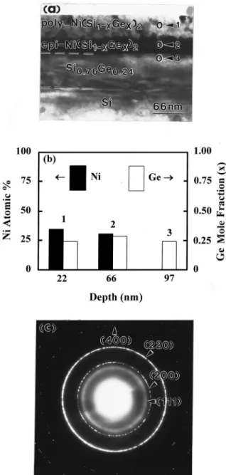
smooth Ni共Si1⫺xGex)2layer was formed as shown in Fig. 6,
in which the upper layer is polycrystalline, while the lower layer is epitaxial. Meanwhile the EDS/XTEM data show that although some Ge tended to segregate down to the lower part of the germanosilicide layer, Ge segregation out of the ger-manosilicide to the underlying Si0.76Ge0.24 films did not
oc-cur. Correspondingly, the XRD pattern of the sample an-nealed at 0.2 J/cm2 for 20 pulses is shown in Fig. 7共b兲.
Evidently, the lattice constant of the unreacted Si0.76Ge0.24 film in the direction perpendicular to the film surface re-mained nearly unchanged in comparison with that of the as-grown Si0.76Ge0.24 film, revealing that no strain relaxation
appeared in the unreacted Si0.76Ge0.24 film. Meanwhile, in
Fig. 7共c兲 the XRD pattern of the sample annealed at 400 °C shows the occurrence of strain relaxation. The aforemen-tioned results have shown that upon annealing at tempera-tures above 300 °C Ge segregation to the unreacted Si0.76Ge0.24film occurred with the extent becoming more
se-vere at higher temperatures. The chemical inhomogeneities present in the surface of the unreacted Si0.76Ge0.24 film may
induce misfit dislocations and hence cause strain relaxation.36 As a consequence, it seems that preventing Ge segregation to the unreacted Si1⫺xGex film can suppress strain relaxation. Similar results have been observed in the Pd/Si0.76Ge0.24 system.
13
For the samples annealed at 0.3 J/cm2 for 5 pulses a single Ni共Si1⫺xGex)2 film was
formed concurrently with Ge segregation to the underlying Si0.76Ge0.24film.
For the Ni/Si1⫺x⫺yGexCy samples annealed at
0.2 J/cm2Ni2共Si1⫺x⫺yGexCy), Ni共Si1⫺x⫺yGexCy), and Ni共Si1⫺x⫺yGexCy)2 were formed for 5, 10, and 30 pulses,
respectively. The Ni共Si1⫺x⫺yGexCy)2layer was very smooth
and no apparent Ge segregation into the underlying Si1⫺x⫺yGexCy film occurred as shown in Fig. 8.
The above results reveal that upon pulsed laser annealing the addition of C to the Si1⫺xGexfilms also retards the phase transformation. In addition, upon multiple pulse laser anneal-ing smooth Ni共Si0.76Ge0.24兲2 and Ni共Si1⫺x⫺yGexCy)2 films
can be grown without showing Ge segregation to the unre-acted Si0.76Ge0.24 films and inducing strain relaxation.
IV. SUMMARY AND CONCLUSIONS
共1兲 For the Ni/Si0.76Ge0.24and Ni/Si1⫺x⫺yGexCysamples an-nealed at a temperature of 200–600 °C Ge segregation to
FIG. 5. 共a兲 XTEM image and 共b兲 the depth profiles of the chemical elements for the Ni/Si0.76Ge0.24sample annealed at 0.3 J/cm
2
.
FIG. 6.共a兲 XTEM image and 共b兲 the depth profiles of the chemical elements for the Ni/Si0.76Ge0.24sample annealed at 0.2 J/cm
2
for 20 pulses,共c兲 DP of the poly-Ni共Si1⫺xGex)2.
the underlying substrates occurred with the extent be-coming more severe at higher annealing temperatures. For the Ni/Si1⫺x⫺yGexCy system the temperatures at which phase transformation and agglomeration occurred were higher in comparison with the Ni/Si0.76Ge0.24
sys-tem.
共2兲 For the Ni/Si0.76Ge0.24 and Ni/Si1⫺x⫺yGexCy samples subjected to pulsed KrF laser annealing the agglomera-tion structure did not occur, but the phase transformaagglomera-tion in the latter was sluggish in comparison with that in the
former. It is evident that C plays an important role on delaying phase transformation upon either vacuum an-nealing or pulsed KrF laser anan-nealing.
共3兲 Multiple pulse laser annealing can produce smooth
Ni共Si0.76Ge0.24兲2 and Ni共Si1⫺x⫺yGexCy)2 films without
inducing Ge segregation and strain relaxation of the un-reacted substrates.
ACKNOWLEDGMENT
This study was supported by Republic of China National Science Council under Contract No. NSC87-2215-E-006-013.
1
S. S. Iyer, G. L. Patton, J. M. Stork, B. S. Meyerson, and D. L. Harame, IEEE Trans. Electron Devices 36, 2043共1989兲.
2S. C. Jain and W. Haynes, Semicond. Sci. Technol. 6, 547共1991兲. 3R. F. Soref, J. Appl. Phys. 70, 2470共1991兲.
4
A. A. Demkov and O. F. Sankey, Phys. Rev. B 48, 2207共1993兲.
5J. L. Regolini, S. Bodnar, J. C. Oberlin, F. Ferrieu, M. Ganneau, B.
Lambert, and P. Bucaud, J. Vac. Sci. Technol. A 12, 1015共1994兲.
6R. D. Thompson, K. N. Tu, J. Angillelo, S. Delage, and S. S. Iyer, J.
Electrochem. Soc. 135, 3161共1988兲.
7
J. S. Luo, W. T. Lin, C. Y. Chang, and W. C. Tsai, J. Appl. Phys. 82, 3621共1997兲.
8J. S. Luo, W. T. Lin, C. Y. Chang, and W. C. Tsai, Mater. Chem. Phys.
54, 160共1998兲.
9
Q. Z. Hong and J. W. Mayer, J. Appl. Phys. 66, 611共1989兲.
10H. K. Liou, X. Wu, U. Gennser, V. P. Kesan, S. S. Iyer, K. N. Tu, and E.
S. Yang, Appl. Phys. Lett. 60, 577共1992兲.
11A. Buxbaum, M. Eizenberg, A. Raizman, and F. Schaffler, Appl. Phys.
Lett. 59, 665共1991兲.
12
A. Buxbuam, E. Zolotoyabko, M. Eizenberg, and F. Schaffler, Thin Solid Films 222, 157共1992兲.
13D. R. Chen, J. S. Luo, W. T. Lin, C. Y. Chang, and P. S. Shin, Appl.
Phys. Lett. 73, 1355共1998兲.
14
O. Thomas, S. Delage, F. M. d’Herule, and G. Scilla, Appl. Phys. Lett. 54, 228共1989兲.
15W. J. Oi, B. Z. Li, W. N. Huang, Z. G. Gu, H. Q. Lu, X. J. Zhang, M.
Zhang, G. S. Dong, D. C. Miller, and R. G. Aitken, J. Appl. Phys. 77, 1086共1995兲.
16
D. B. Aldrich, Y. L. Chen, D. E. Sayers, R. J. Nemanich, S. P. Ashburn, and M. C. Ozturk, J. Appl. Phys. 77, 5107共1995兲.
17D. B. Aldrich, H. L. Heck, Y. L. Chen, D. E. Sayers, and R. J. Nemanich,
J. Appl. Phys. 78, 4958共1995兲.
18
A. Eyal, R. Brener, R. Beserman, M. Eizenberg, Z. Atzmon, D. J. Smith, and J. W. Mayer, Appl. Phys. Lett. 69, 64共1996兲.
19W. Freiman, A. Eyal, Y. L. Khait, R. Beserman, and K. Dettmer, Appl.
Phys. Lett. 69, 3821共1996兲.
20J. S. Luo, W. T. Lin, C. Y. Chang, W. C. Tsai, and S. J. Wang, Mater.
Chem. Phys. 48, 140共1997兲.
21M. C. Ridgway, R. G. Elliman, N. Hauser, J. M. Baribeau, and T. E.
Jackman, Mater. Res. Soc. Symp. Proc. 260, 857共1992兲.
22F. Lin, G. Sarcona, M. K. Hatalis, A. F. Cserhati, E. Austin, and D. W.
Greve, Thin Solid Films 250, 20共1994兲.
23
Z. Wang, Y. L. Chen, H. Ying, R. J. Nemanich, and D. E. Sayer, Mater. Res. Soc. Symp. Proc. 320, 397共1994兲.
24J. S. Luo, Y. L. Hang, W. T. Lin, C. Y. Chang, and P. S. Shih, J. Mater.
Res. 14, 3433共1999兲.
25
V. Aubry, F. Meyer, R. Laval, C. Clerc, P. Warren, and D. Dutartre, Mater. Res. Soc. Symp. Proc. 320, 299共1994兲.
26V. Aubry, F. Meyer, R. Laval, C. Clerc, P. Warren, and D. Dutartre,
Appl. Surf. Sci. 73, 285共1993兲.
27Q. Z. Hong and J. W. Mayer, Mater. Res. Soc. Symp. Proc. 181, 145
共1990兲.
28E. J. Jaquez, A. E. Bair, and T. L. Alford, Appl. Phys. Lett. 70, 874
共1997兲.
29J. S. Luo, W. T. Lin, C. Y. Chang, and P. S. Shih, Thin Solid Films 346,
207共1999兲. FIG. 8. 共a兲 XTEM image and 共b兲 the depth profiles of the chemical elements
for the Ni/Si1⫺x⫺yGexCysample annealed at 0.2 J/cm
2
for 30 pulses. FIG. 7. XRD patterns of共a兲 the as-grown Si0.76Ge0.24film,共b兲 the unreacted
Si0.76Ge0.24film after annealing at 0.2 J/cm 2
for 20 pulses, and共c兲 the un-reacted Si0.76Ge0.24film after annealing at 400 °C.
30Z. Wang, D. B. Aldrich, R. J. Nemanich, and D. E. Sayers, J. Appl. Phys.
82, 2342共1997兲.
31R. A. Donaton and K. Maex, A. Vantomme, G. Langouche, Y. Morciaux,
A. St. Amour, and J. C. Sturm, Appl. Phys. Lett. 70, 1266共1997兲.
32V. Aubry-Fortuna, A. Eyal, O. Chaix-Pluchery, M. Barthula, F. Meyer,
and M. Eizenberg, Appl. Phys. Lett. 73, 1248共1998兲.
33
Cohesion in Metals: Transition Metal Alloys, edited by F. R. Deboer, R.
Boom, W. C. Mattens, A. R. Miedema, and A. K. Niessen共North Hol-land, Amsterdam,共1988兲.
34J. S. Luo, W. T. Lin, C. Y. Chang, P. S. Shin, F. M. Pan, and T. C. Chang,
Mater. Chem. Phys. 60, 58共1999兲.
35W. Kern and D. A. Puotinen, RCA Rev. 31, 187共1970兲. 36
A. Buxbaum, E. Zolotoyabko, M. Eizenberg, and F. Schaffler, Thin Solid Films 222, 157共1992兲.