A 44-GHz High-Linearity MMIC Medium Power Amplifier
with a Low-loss Built-in Linearizer
Jeng-Han Tsai, Hong-Yeh Chang, Pei-Si Wu, Tian-Wei Huang, and Huei Wang
Department of Electrical Engineering and Graduate Institute of Communication Engineering,
National Taiwan University, Taipei, Taiwan, 106, R.O.C.
Abstract — This paper presents a 44-GHz MMIC medium
power amplifier with a low-loss built-in linearizer using a 0.15-µm GaAs HEMT process. The proposed cold-mode HEMT linearizer can enhance the linearity of the power amplifier with a low insertion loss, a compact die-size, and zero dc consumption. These advantages make the linearizer more suitable for millimeter-wave applications. The experimental results show that the medium power amplifier output spectrum re-growth can be suppressed by 7-9 dB at 44 GHz. In addition, the EVM of the QPSK and 16-QAM modulated signal can be reduced from 4.5% to 3.7% and 10.8% to 7.4% respectively. To the best of our knowledge, this is the first attempt of using pre-distortion linearization techniques in millimeter-wave bands.
Index Terms — Linearizer, millimeter-wave (MMW),
monolithic microwave integrated circuit (MMIC), nonlinear, power amplifier (PA).
I. INTRODUCTION
In millimeter-wave (MMW) frequency bands, there are increasing demands for high-data-rate digital communications, such as Gigabits MMW broadband systems [1] and satellite communication systems [2]. These high-data-rate digital communication systems tend to use complex digital modulation schemes like QPSK and 16-QAM, which requires a high-linearity power amplifier to reduce the spectral re-growth. Nevertheless the output power in MMW frequency is an expensive resource. Therefore, to satisfy the stringent linearity requirements of the power amplifier under the best available power, the linearization techniques are used to reduce the amount of power back-off.
One of the solutions to improve the linearity of the power amplifier is using a pre-distortion linearizer [3]. It has the advantages of smaller size, less complexity, lower cost than other linearization techniques. Various pre-distortion linearizers, such as diode linearizer and passive FET, have been applied to microwave applications under 20 GHz in [4]-[6]. Nevertheless, these linearizers [5], [6] usually cause high insertion losses, 6-11 dB, which means, we need to add an extra buffer amplifier to compensate the power gain loss in microwave frequencies. Furthermore, these microwave linearizers require complex bias circuits, which increase the die area.
In this paper, a 44-GHz MMIC medium power amplifier with a low-loss built-in linearizer using cold mode HEMT is
presented. We place a shunt cold mode HEMT, whose Vds equal to zero, before the input of the amplifier. Using this topology, we can feed the gate bias of the amplification transistor directly through the built-in linearizer without additional bias circuits. Furthermore, the insertion loss cause by the shunt linearizer is less than 2 dB, so we can maintain the gain performance of the MMW amplifier. By varying the gate bias of the shunt cold mode HEMT, the gain expansion performance of the linearizer can be adjusted easily. The proposed linearizer enhances the linearity of the power amplifier with a low insertion loss, a compact die-size, and zero dc consumption. Therefore it is suitable for MMW frequency applications.
II. TECHNOLOGY
In the amplifier design, we used a 0.15-µm GaAs HEMT MMIC process on 100-µm GaAs substrate provided by WIN Semiconductors. The unit current gain frequency (fT) of the device is about 85 GHz, and the maximum oscillation frequency (fmax) is over 200 GHz. Typical breakdown voltage is 10V and the peak of transconductance (Gm) is 495 mS/mm. Other passive components such as thin-film resistors, MIM capacitors, spiral inductors, and air-bridges are available. The 6” wafer is thinned down to 4-mil for the gold plating of the backside, and slot via holes are used for dc grounding [7].
III. CIRCUIT DESIGN AND FABRICATION
Usually, a power amplifier shows gain compression at high power levels, which results in the signal distortion. The linearizer can provide gain expansion to compensate the distortion of the amplifier. Fig. 1 is the schematic of the amplifier with a built-in linearizer proposed in this paper. The common source (CS) connected transistor HEMT1 is the amplification stage, which employs a two-finger 150-µm HEMT device. Before the input of the HEMT1, a shunted transistor HEMT2 is added as the linearizer, which also employs a two-finger 150-µm HEMT device. The cold mode operation transistor HEMT2 has no drain bias (Vds= 0 V). Therefore we can bias the amplification transistor HEMT1 directly through the linearizer with Vg1=Vd2. At cold mode operation, the transistor HEMT2 is equivalent to a variable
drain-to-source resistor (Rds) controlled through the gate bias (Vg2). When the input power is increased, the value of Rds increases simultaneously, due to the positive gain slope of the linearizer. We can use this gain expansion characteristic to compensate the gain compression of the power amplifiers. The insertion loss caused by the shunt HEMT is depended on the value of Rds. We must choose the suitable device size and gate bias to reduce the insertion loss, and maintain the positive gain slope characteristic of the linearizer.
The output matching network was designed according to the power contour to achieve the maximum RF output power. The input of PA is simply conjugate matched. And the input and output matching networks are realized with open and short stubs. The 0.4-pF capacitors are used for in-band RF bypass network. Several shunt RC bypass networks are used to ensure low frequency stability and out-of-band RF bypass. The input and output of PA have on-chip DC-blocking capacitors. The passive circuits include the transmission line discontinuities and capacitors, were simulated by a full-wave EM simulator (Sonnet software) [8]. The whole circuit of the amplifier with a built-in linearizer was simulated with Agilent ADS. It draws total 35-mA DC current from a 4-V supply voltage. Vg1 Vd1 Vgc Vd2 HEMT1 HEMT2 Vtest
Fig. 1. Schematic of the 44-GHz medium power amplifier with a built-in linearizer.
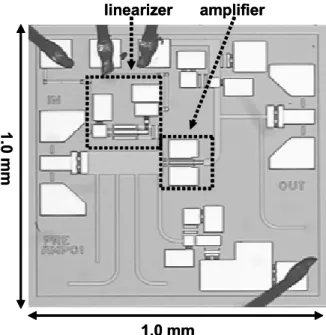
IV.APPLICATION TO LINEARIZED MEDIUM POWER AMPLIFIER To verify the performance of the presented linearizer, a 44-GHz MMIC medium power amplifier with a low-loss built-in linearizer has been fabricated. Fig. 2 illustrates the chip photo of the MMIC. The physical size of this MMIC is 1.0-mm x 1.0-mm including input and output matching networks, DC bias networks, on-wafer probing pads, and an integrated linearizer. Fig. 3 shows the 40 to 50 GHz S-parameter of the medium power amplifier with a built-in linearizer, and the simulation and measurement results have excellent
agreements. It demonstrates 8-dB measured small signal gain at Vd1= 4 V, Vd2=Vg1= -0.5 V and Vgc= -1.5 V.
The maximum available gain (MAG) of the two-finger 150-µm HEMT transistor simulation results also plotted in Fig. 3, which shows that MAG is 10.5 dB at 44 GHz. We also use the same transistor to design a similar common source amplifier without a built-in linearizer, which demonstrates 9.5-dB small signal gain at 44 GHz from the simulation results. Therefore, we can calculate the insertion loss caused by the low-loss built-in linearizer is less than 2 dB. We compare the insertion loss of different linearizers in TableI, which shows the shunt cold mode HEMT linearizer topology has lower insertion loss than the previously published Ku-Band linearizers. linearizer 1.0 mm 1. 0 m m amplifier linearizer 1.0 mm 1. 0 m m amplifier
Fig. 2. Photograph of the MMIC medium power amplifier with a built-in linearizer. 40 41 42 43 44 45 46 47 48 49 50 Frequency (GHz) S-parameters -15 -10 -5 0 5 10 15 G ai n & Retu rn L o ss es (d B ) ○
S21
△S22
□S11
◇MAG
40 41 42 43 44 45 46 47 48 49 50 Frequency (GHz) S-parameters -15 -10 -5 0 5 10 15 G ai n & Retu rn L o ss es (d B ) ○S21
△S22
□S11
◇MAG
Fig. 3. 40 to 50 GHz S-parameter simulation (non-connected lines) and measurement results (connected lines) at Vd1= 4 V, Vd2=Vg1= -0.5 V and Vgc= -1.5 V.
TABLE I
COMPARISON OF LINEARIZER INSERTION LOSSES Ref. Frequency Insertion Loss Topology
[5] 18 GHz 11 dB Parallel Diode
[6] 11-13 GHz 6 dB Series
Common Gate FET This
Work
44 GHz < 2 dB Shunt
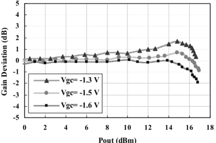
Cold Mode HEMT Fig. 4 shows the measured gain deviation characteristics of the medium power amplifier with a built-in linearizer at difference Vgc. We vary the gate bias (Vgc) of the shunt cold mode HEMT to adjust the gain expansion performance of the linearizer. From Fig. 4, we can analyze the linear power region of the medium power amplifier with the linearizer turn-on. We try to select the bias point which provides both the appropriate gain expansion and the linear power region of the PA. According to Fig. 4, we select Vgc= -1.5 V for the linearizer bias point in this paper, which provides the best linear power performance among these three curves.
In order to test and verify the functions of the linearizer, we turn off the linearizer and feed the gate bias of the amplifier through Vtest in Fig. 1. Then we turn on the linearizer with bias at Vd2= -0.5 V and Vgc= -1.5 V. Fig. 5 demonstrates the output power and gain versus input power measurement results of the amplifier with and without linearizer at 44 GHz. The saturation output power of the amplifier is 17 dBm. It is observed that the gain compression of the amplifier has been compensated by the built-in linearizer. Then we would use digital modulation signal to test the medium power amplifier with a built-in linearizer under these two difference conditions.
-5 -4 -3 -2 -1 0 1 2 3 4 5 0 2 4 6 8 10 12 14 16 18 Pout (dBm) G ain D ev ia tio n ( d B ) Vgc= -1.3 V Vgc= -1.5 V Vgc= -1.6 V
Fig. 4. Measured gain deviation characteristics of the medium power amplifier with a built-in linearizer at difference Vgc.
-15 -10 -5 0 5 10 15 -10 -5 0 5 10 15 20 Po ut (dBm ) & G ai n (dB) Pin (dB m ) L inearizer off L inearizer on at V g1=-0.5 V , V gc=-1.5 V
Fig. 5. Measured output power and gain versus input power of the medium power amplifer at 44 GHz
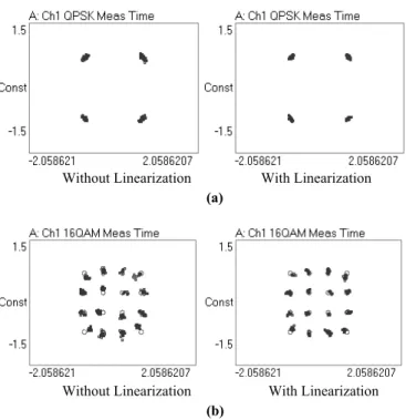
To test this medium power amplifier with a built-in linearizer under digital modulation signal, we use Agilent E4438C vector signal generator to generate the QPSK and 16-QAM digital modulation signal with symbol rate of 1Msps at 6 GHz. We can convert the digital signal into 44 GHz by using a sub-harmonically pumped mixer, which has a fundamental LO at 19 GHz. Fig. 6 plots the QPSK spectrum measurement results with a channel power of 13 dBm in 1-MHz channel bandwidth at 44 GHz. We can observe the spectral re-growth is suppressed by 7-9 dB after linearization. Then we down convert the 44-GHz digital modulated signal by Agilent E4448A spectrum analyzer, and measure the modulation quality through Agilent VSA. Fig. 7 plots the QPSK and 16-QAM constellation diagram. The points in the 16-QAM constellation can be spread out more uniformly into a “square” after linearization. The EVM of the QPSK and 16-QAM modulation signal can be reduced from 4.5% to 3.7% and 10.8% to 7.4% respectively. Therefore the amplifier with a low-loss built-in linearizer has better linearity than the amplifier without linearizer.
Fig. 6. QPSK spectrum measurement results with a channel power of 13 dBm in 1-MHz channel bandwidth at 44 GHz
Without Linearization With Linearization (a)
Without Linearization With Linearization (b)
Fig. 7. (a) QPSK constellation diagram measurement results with a channel power of 13 dBm in 1 MHz channel bandwidth at 44 GHz. (b) 16-QAM constellation diagram measurement results with a channel power of 14 dBm in 1 MHz channel bandwidth at 44 GHz..
V.CONCLUSION
A 44-GHz MMIC medium power amplifier with a low-loss built-in linearizer using cold mode HEMT in a 0.15-µm GaAs HEMT MMIC process has been developed. The proposed built-in linearizer provides gain expansion to compensate the gain compression in power amplifier non-linear region. In addition, the built-in linearizer also has advantages of low insertion loss (< 2 dB), compact die-size and zero dc consumption. Therefore it is attractive for millimeter-wave power amplifier applications. According to the experimental results, it is confirmed that the proposed linearizer improves the linearity of the amplifier. The QPSK modulated signal
spectrum re-growth is suppressed by 7-9 dB with linearization. The EVM of the QPSK and 16-QAM modulated signal can be reduced from 4.5% to 3.7% and 10.8% to 7.4% respectively.
ACKNOWLEDGEMENT
This work is supported in part by National Science Council (NSC 93 - 2219 - E - 002 – 025). The MMIC chip is fabricated by WIN Semiconductors through the Chip Implementation Center (CIC), Taiwan, ROC.
REFERENCES
[1] Katsutoshi TSUKAMOTO, et.al., “Development of Gigabit Millimeter-Wave Broadband Wireless Acces System - System Overview -,” in 2003 Asia-Pacific Microwave Conf. Proc., TC5_01, Dec. 2003.
[2] B. Hughes, J. Orr, G. Martin, “MMIC 20 GHz low-noise and 44 GHz power amplifiers for phased array communication antennas designed for manufacturability,” in IEEE GaAs IC Symp. Dig., pp. 367-370, Oct. 1993.
[3] Y. Jaehyok, Y. Youngoo, P. Myungkyu, K. Wonwoo, K. Bumman, “Analog predistortion linearizer for high-power RF amplifiers,” IEEE Trans. Microwave Theory & Tech., vol. 48, no. 12, pp. 2709-2713, Dec. 2000.
[4] P. Narozny, H. Tobler, G. K. Kornfeld, R. A. Nunn, B. Adelseck, M. Ludwig, G. Eggers, “Pseudomorphic Ku-band GaAs HFET linearizer preamplifier front end for satellite TWT-amplifiers, ” in IEEE GaAs IC Symp. Dig., pp. 292-295, Oct. 1995.
[5] K. Yamauchi, M. Nakayama, Y. Ikeda, H. Nakaguro, N. Kadowaki, T. Araki, “An 18 GHz-band MMIC linearizer using a parallel diode with a bias feed resistance and a parallel capacitor,” 2000 IEEE MTT-S Int. Microwave Symp. Dig., vol. 3, pp. 1507-1510, Jun. 2000.
[6] A. Katz, S. Moochalla, J. Klatskin, “Passive FET MMIC linearizers for C, X, and Ku-band satellite applications,” 1993 IEEE MTT-S Int. Microwave Symp. Dig., vol. 1, pp. 353-356, Jun. 1993.
[7] WIN, Inc., 0.15µm InGaAs pHEMT Power Device Model Handbook, 2003.
[8] Sonnet Software Inc., Sonnet User’s Manual, Release 6.0 Liverpoll, NY, Apr. 1999.