Impacts of NBTI/PBTI on Timing Control Circuits
and Degradation Tolerant Design in Nanoscale
CMOS SRAM
Hao-I. Yang, Student Member, IEEE, Shyh-Chyi Yang, Wei Hwang, Life Fellow, IEEE, and
Ching-Te Chuang, Fellow, IEEE
Abstract—Negative-bias temperature instability (NBTI) and positive-bias temperature instability (PBTI) weaken PFET and NFET over the lifetime of usage, leading to performance and reliability degradation of nanoscale CMOS SRAM. In addition, most of the state-of-the-art SRAM designs employ replica timing control circuit to mitigate the effects of leakage and process vari-ation, optimize the performance, and reduce power consumption. NBTI and PBTI also degrade the timing control circuits and may render them ineffective. In this paper, we provide comprehensive analyses on the impacts of NBTI and PBTI on a two-port 8T SRAM design, including the stability and Write margin of the cell, Read/Write access paths, and replica timing control circuits. We show, for the first time, that because the Read/Write replica timing control circuits are activated in every Read/Write cycle, they exhibit distinctively different degradation behavior from the normal array access paths, resulting in degradation of timing control and performance. We also discuss degradation tolerant design techniques to mitigate the performance and reliability degradation induced by NBTI/PBTI.
Index Terms—Negative bias temperature instability (NBTI), positive bias temperature instability (PBTI), reliability, replica timing control circuit, SRAM.
I. INTRODUCTION
N
ANOSCALE SRAM design must ensure robust opera-tions against large leakage, PVT variation, and degra-dation over the usage lifetime. The negative-bias temperature instability (NBTI) has long been known to be a serious con-cern for scaled PFET. With the introduction of high-k metal-gate device and its associated charge-trapping related threshold voltage instability, the positive-bias temperature insta-bility (PBTI) has become more significant in NFET [1], [2]. The NBTI and PBTI effects cause the threshold voltage of transistors to drift with stress time, thus weakening PFET and NFET respectively.SRAM design composes of logic control circuits and bit cells. Logic control circuits include decoders and Read/Write access timing control circuits. In order to trace real word-line and
bit-Manuscript received May 26, 2010; revised September 19, 2010; accepted November 08, 2010. Date of publication January 06, 2011; date of current ver-sion May 27, 2011. This work was supported in part by the National Science Council under Contract NSC 98-2221-E-009-112, and in part by the Ministry of Economic Affairs, under Project MOEA 99-EC-17-A-01-S1-124. This paper was recommended by Associate Editor A. Strollo.
The authors are with the Department of Electronics Engineering and Institute of Electronics, National Chiao-Tung University, Hsinchu 300, Taiwan (e-mail: [email protected]).
Digital Object Identifier 10.1109/TCSI.2010.2096112
line delay, and Write-time of bit cells, replica circuits are often used in SRAM timing control circuit. With serious transistors’ geometry/dimension variations and intrinsic fluctuations, the mismatch is more serious in SRAM bit cells. Monte Carlo simulations and statistical methods are needed to design a robust bit cell [3], [4]. With the drifts induced by NBTI and PBTI, and mismatches among individual cell transistors be-come more serious, leading to degradation of stability and the already poor design margin [5]. The Read latency of a bit cell is more sensitive to PBTI and increases with stress time, whereas the Write margin (WM) may improve or degrade depending on the signal (stress) probability of the bit cell [6]–[8]. of bit cells has also been shown to degrade with time [9]. Fur-thermore, the design of SRAM logic control circuit should also consider the variation and leakage effect in order to im-prove SRAM access failure rate [10], [11]. These circuits are also under NBTI and PBTI stress. It leads to drifts of trip points of logic circuits and degradation of signal propagation delays. The drifts of trip points and degradation of propagation delays depend on the input pattern [12]–[15]. As a result, timing mis-match between bit cells and SRAM logic control circuits oc-curs, leading to access performance degradation and unreliable access operations [16].
In the logic circuit, transistor sizing, optimizing the node activity, lowering operating temperature, adaptively changing by using body biasing, and dynamically adjusting supply voltage could be used to mitigate performance and reliability degradation induced by NBTI and PBTI. Transistor sizing reserves extra margin for drift by oversizing transistors [12], [13]. Optimizing the node activity mitigates drift by decreasing the stress time of transistors [14], [15]. Both transistor sizing and optimizing the node activity require accurate estimation of the performance degradation induced by NBTI/PBTI. The drift induced by NBTI/PBTI can also be reduced by using adaptive body biasing according to the information from on-chip sensors [17]. The efficiency of this mechanism depends on the effectiveness of body biasing. Lowering the supply voltage mitigates drift; however, the delay of logic circuits becomes more sensitive to drift with reduced supply voltage [14], [15]. Dynamically adjusting the supply voltage level according to the circuit operation mode (Active or Standby) could resolve the dilemma of statically lowering the supply voltage, but its efficiency decreases with higher circuit activities [17]. On the other hand, periodically flipping the cell, reducing the Standby cell supply voltage, raising the Standby cell virtual ground voltage, and adaptively
of these two mechanisms is affected by the activity factor of the SRAM array. If the SRAM array has high activity, their efficiency decreases. drift can also reduces by adaptive body biasing according to the information from on-chip sensors [17]. Similar to that in logic circuits, its efficiency depends on the effectiveness of body biasing.
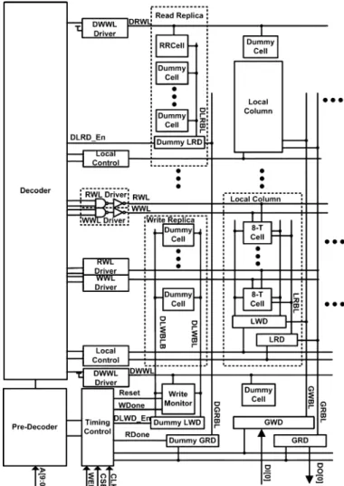
In this paper, we investigate the impacts of NBTI and PBTI on the stability and WM of a two-port 8T SRAM design. We then provide comprehensive analyses on the degradations of SRAM Read access and Write performance with hierarchical bit-line and Read/Write replica timing control circuits (Fig. 1). We show that because the Read/Write replica timing control cir-cuits are activated in every Read/Write cycle, they exhibit dis-tinctively different degradation behavior from the normal array access paths, resulting in degradation of timing control and per-formance. We also show that Read access degradation domi-nates the SRAM performance degradation, and Write Half-Se-lect stability degradation dominates the stability of 8T SRAM cell. Further, we show that raising the Standby Virtual Ground voltage of the 8T cell’s Read buffer mitigates the Read perfor-mance degradation, and data-retention power-gating techniques and dual- 8T cell can be used to mitigate the stability degra-dation of bit cells. Hierarchical Read/Write scheme can improve the efficiency of these techniques.
The rest of this paper is organized as follows: Section II describes the NBTI and PBTI models used in conjunction with PTM 32 nm node high- metal-gate technology model [19]. Section III investigates the impacts of NBTI/PBTI on 8T SRAM cells. Section IV presents a comprehensive analysis on the degradations of SRAM logic control circuits, including decoder, Read/Write access paths, and replica timing-control circuits. The NBTI/PBTI tolerant design schemes are discussed in Section V. Finally, we conclude the paper in Section VI.
II. NBTIANDPBTI MODELS
drifts induced by NBTI and PBTI depend on the stress voltage, temperature, and stress time. They increase with stress time and saturate after a long time stress. The saturated drift is more severe under higher stress voltage/temperature.
NBTI renders of PFET more negative with stress time due to generation of Si and SiO interface traps [14], [20]–[22]. When of PFET is negative (stress phase), holes in the in-version layer interact with and break Si-H bonds at the Si and SiO interface. H or H diffuses into the SiO , and undesir-able Si dangling bonds generate at the interface, thus leading to the increase in . When the stress condition is removed , H or H diffuses back to the interface and passi-vates dangling Si- bonds, causing the decrease of (re-covery phase). Therefore, the PFET life time under alternating
Fig. 1. SRAM with hierarchical bit-line and Read/Write-Replica Timing Con-trol circuits.
stress is longer than that predicted by using static stress mea-surements. The corresponding effect for NFET is PBTI. It is in general quite small and can be neglected for oxide/poly-gate devices. However, NFET with high-k gate exhibit significant charge trapping and thus long-term drift as well [1], [2]. Typically, drifts induced by NBTI and PBTI would satu-rate when the stress time is around to s [1], [2], [23].
The drift of PFET (NFET) due to NBTI (PBTI) under static stress can be described by dc reaction-diffusion (RD) framework [5], [14], [15], [20]–[22]. If transistors are under alternative stress, the dc RD model should be modified to an ac RD model [4], [12], [13]
(1) where the prefactor is a function of stress frequency (f) and stress (or signal) probability (S), and is a technology-de-pendent constant. can be expressed as [14]
(2) where is the gate oxide thickness, is the gate elec-tric field, k is Boltzmann constant, and T is temperature. The
Fig. 2. drifts induced by NBTI and PBTI using RD framework cali-brated with published data [1], [2]. for High-k metal gate
for poly gate .
constant, A, is calibrated with the hardware data results in [1], [2]. Fig. 2 shows the drift induced by dc NBTI and PBTI stress calculated by incorporating RD framework with PTM 32 nm and PTM High-k 32 nm device models [19]. According to the results of [22], [24], the impact of the signal frequency on drift is relatively insignificant. Thus, we neglect the ef-fect of signal frequency, and analyze cases with various signal (stress) probabilities in our analysis. The prefactors of ac RD framework in our analyses are from [4].
The following sections present the detail simulation results based on BSIM 32 nm Predictive High-k Metal-Gate Model. The supply voltage of the SRAM arrays is 0.9 V, and the tem-perature is 125 C. The drift due to NBTI and PBTI are based on ac RD framework. The ranges of values for sheet re-sistance and wire capacitance are based on scaling/extrapolation from UMC 65 nm CMOS process and ITRS Roadmap [25].
III. IMPACTS ON8T TWO-PORTSRAM CELLS
An 8T two-port SRAM cell is formed by combining a con-ventional 6T bit cell and a stacked NFET Read buffer, as shown in Fig. 3. Its Read port and Write port are separated; therefore, it is possible to optimize SRAM Read and Write paths respec-tively. The 8T cell has no Read disturb problem because its Read access path is isolated from the cell storage nodes. However, it still has Write Half-Select disturb problem with bit-interleaving architecture. The Write operation of the 8T cell is performed like that of a 6t cell, and the Write Half-Select disturb of the 8T cell is the same as the access Half-Select disturb of a con-ventional 6T cell. Consequently, the impact of NBTI and PBTI on the 8T cell can cover the impact on a 6T cell. Furthermore, the 8T cell is the most promising candidate to replace the con-ventional 6T cell in deep sub-100 nm technology, as it enables continuing cell size scaling and would potentially have smaller area than 6T cell below 32 nm [26]. Therefore, the analysis and understanding of the NBTI and PBTI impact on the 8T cell can not only provide the understanding of the impacts on a conven-tional 6T cell, but also help designers to optimize 8T SRAM
Fig. 3. Two-port 8T SRAM cell.
in deep sub-100 nm technology. In the rest of this section, we will analyze the impacts of NBTI and PBTI on the Read oper-ation, Write operoper-ation, and stability of the 8T cell. We assume the length of Read bitline (RBL) and Write bitline (WBL) pairs are 16-bit (short bit-line to mitigate leakage, variation, and noise coupling) for Read/Write delay analyses.
A. Read Operation
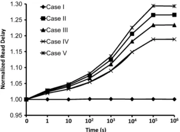
During Read cycles, the RWL of the selected cell turns on, and the selected RBL discharges through the Read buffer of the selected cell. Read delay of an 8T cell can be defined as the time from RWL rises to 50% to the time RBL discharges to 50%. Table I summarizes 5 different cell signal (stress) probability cases, and Fig. 4 shows the relation between Read delay and PBTI stress time. Clearly, long term degradation of Read delay happens if the signal probability of the selected cell is not 100% (Q does not always store logic “1”). The Read buffer is a NFET stack formed by MR1 and MR2. The Read access transistor, MR1, only experiences PBTI stress when the cell is selected during Read cycles, thus the drift of MR1 is negligible. However, MR2 is under PBTI stress if the cell stores logic “0” . Thus, if the signal (stress) probability is not 100%, MR2 would be stressed, and the drift of MR2 degrades the Read current and RBL discharging time. The drift of MR2 also results in decrease of RBL leakage current with time. The Read delay is insensitive to NBTI as the Read buffer is com-posed only of NFETs. Although NBTI may induce drift of ML2 drift and decrease the trip point of the inverter (ML2 and MD2), the cell storage node voltage level is not affected when the WWL is not selected. Consequently, NBTI has no impact on Read delay of 8T cells.
B. Write Operation
When an 8T cell is under Write operation, its WWL turns on. The cell storage node holding logic “1” discharges through the access NFET first. Once the node originally storing logic “1” is pulled down below the trip voltage of the opposite in-verter, the cross-coupled feedback inverter action kicks in, and the node storing logic “0” charges towards logic “1” through the pull-up PFET to complete the Write operation. The WM can be defined as the highest WBL voltage level that can flip
Fig. 4. Read delay versus usage (stress) time under PBTI. TABLE I
SIGNAL(STRESS) PROBABILITYVERSUSWRITEMARGIN ANDREADDELAY
SUMMARY
the state of a SRAM cell during Write cycles. If WM decreases, the Write delay of the cell increases, and Write failure rate also increases. If WM deteriorates, data may not be written into the cell. Fig. 5 shows the combining impacts of NBTI and PBTI on WM of the selected cell. WM of a SRAM cell improves in most cases except for Case I. This is because when a cell is af-fected by NBTI and the cell signal (stress) probability is not 100% (0%), both PFET loading transistors become weaker. A weaker PFET facilitates the initial discharging of the logic “1” storage node. In contrast, a weaker pull-up PFET impedes the subsequent pull-up of the logic “0” storage node. Since the ini-tial discharging of the logic “1” storage node tends to be the dominating factor for Write operation, WM improves with both PFETs weakened. However, when the cell signal (stress) proba-bility is 100% (0%) (as in Case I), only one PFET loading tran-sistor becomes weaker. For the worst case pattern, the PFET holding the original logic “1” storage node is not stressed/weak-ened, so the pull down of the node is not getting easier. The PFET corresponding to the original logic “0” storage node, how-ever, would be fully stressed/weakened, and thus slowing down the charging of its storage node to logic “1” during Write opera-tion and degrading the WM. Fig. 5 shows that Case I has about 10% WM degradation when the usage (stress) time is sec-onds. It implies that the Write failure rate of the SARM would increase if process variations are also considered. Notice that the Write access transistors, MA1 and MA2, only experience PBTI stress when the cell is selected during Write cycles, thus their drifts are negligible. Also, PBTI stress weakens cell pull-down NFET (MD1 and MD2), thus raising the cell inverter trip voltage and improving the WM.
Fig. 5. WM versus usage (stress) time under NBTI/PBTI.
C. Cell Stability
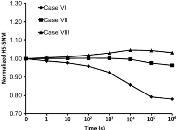
Write Half-Select Static Noise Margin (HS-SNM) dominates the stability of 8T SRAM. During Read cycles, the WWL of the selected cell is off and the Read-SNM (RSNM) of the cell is the same as its Hold-SNM (HSNM). Whereas, in bit-interleaving architecture, half-select cells would experience 6T Read-like disturb during Write cycle. Consequently, Write HS-SNM of 8T cell is worse than its RSNM.
HS-SNM of a cell can be defined as the voltage difference be-tween the maximum disturb cell on storage nodes and the min-imum trip voltage of the cell inverters in half-select cells during Write cycles. Trip points of the cell inverters are determined by the strength ratio of the PFET loading transistor and NFET driving transistor. The strength of NFET driving transistor is usually larger than that of PFET loading transistor. Thus, trip points of cell inverters are typically more sensitive to PBTI ef-fect. Furthermore, the Write half-select disturb is determined by the strength ratio of Write access transistors and NFET driving transistors. Hence, PBTI has a much more significant effect on the Half-Select Static Noise Margin (HS-SNM) than NBTI. Again, the drifts of Write access transistors are negligible since they are stressed only when the WWL is selected during Write cycles. When the cell signal (stress) probability is about 50%, both Write half-select disturb and trip points of cell in-verters increase.
As the NFET driving transistor for the logic “0” storage node is fully on, the increase of Write half-select disturb is smaller than the increase of the trip voltage of the opposite inverter where the NFET driving transistor is off. Thus, Write HS-SNM improves when of both NFET driving transistors increase (Case VIII in Table II) as shown in Fig. 6. In contrast, if the signal (stress) probability is skewed (Case VI and Case VII in Table II), Write half-select disturb would dominate for the worst-case pattern, and Write HS-SNM would degrade with the stress time.
IV. IMPACTS ONSRAM READ/WRITEACCESSPATHS AND
REPLICATIMINGCONTROLCIRCUITS
In this section, we investigate the impacts of NBTI and PBTI on Read and Write access paths of an 8T SRAM design with
Fig. 6. Write HS-SNM versus usage (stress) time under NBTI/PBTI. TABLE II
SIGNAL(STRESS) PROBABILITYVERSUSWRITEHS-SNM SUMMARY
TABLE III
READ/WRITEACCESSANALYSISCASEDEFINITION
hierarchical bit-line (BL) and Read/Write replica timing control circuits. The hierarchical BL structure and replica timing control are widely used in the state-of-the-art SRAM designs to mitigate leakage and variations, and to improve access performance [27]. In our analysis, we investigate impacts of NBTI and PBTI on a 1024 128 bits hierarchical 8T SRAM macro as shown in Fig. 1. The local BL length is 16-bit, and there are 64 local blocks on a global Read-BL (GRBL). The WL length is 128-bit. Read and Write-replica circuits are employed for access timing control. They respectively ensure that the RWL pulse width and WWL pulse width are wide enough for successful Read and Write operations. They also turn off the selected RWL or WWL as early as possible to minimize power consumption and to im-prove SRAM performance (cycle time). The operating voltage of the SRAM is 0.9 V, and its maximum operating frequency is 1.5 GHz. Table III summarizes the three cases used in analyzing the impacts of NBTI/PBTI on SRAM access degradations.
A. Read Access
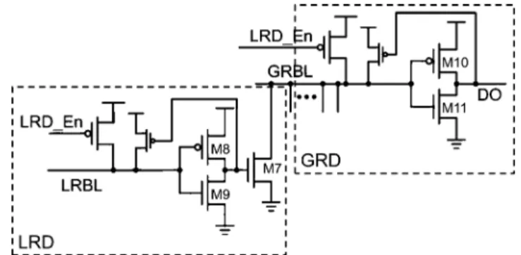
Referring to Fig. 1, when the SRAM is not performing Read operation, precharge circuits in Local Read Driver (LRD) and Global Read Driver (GRD) maintain voltage levels of local Read-BL (LRBL) and Global Read-BL (GRBL) at VDD.
During Read cycles, the timing control unit informs the de-coder to turn off precharge circuits in LRDs and GRDs. The timing control unit also fires up the decoder to turn on the selected Read WL (RWL) and the Dummy RWL (DRWL) of Read-Replica circuit. The Read-Replica cell (RRCell) stores logic “0,” and the Dummy Local RBL (DLRBL) starts to discharge. The signal propagates through the Dummy LRD (DLRD), Dummy GRBL (DGRBL), and the Dummy GRD (DGRD). After the signal, RDone, becomes logic “1,” the timing control unit informs the decoder to turn off the selected RWL and DRWL. The decoder also enables LRDs and GRDs to charge the LRBLs and GRBLs to complete the Read cycle.
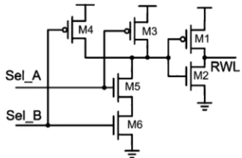
Fig. 7(a) shows the combined impacts of NBTI and PBTI on the turning-on delays of RWL (dash line) and DRWL (solid line) when the SRAM operates at its maximum frequency (1.5 GHz). Referring to Fig. 1, we measure the RWL delay from CLK to RWL (the output of RWL Driver), and we measure the DRWL delay from CLK to DRWL (the output of DRWL Driver). The turning-on delay of the selected RWL decreases with usage time, while the delay of DRWL increases with usage time. This phenomenon can be explained by using an example of WL driver shown in Fig. 8. When the WL driver turns off (i.e., in Standby), M2 and (M3 or M4) become weaker due to PBTI and NBTI stress, respectively. When the WL driver turns on (Active), M1 and M5/M6 are stressed and become weaker. Thus, if the WL driver stays long time in Standby phase, M1 and M5/M6 are seldom stressed and their strengths remain unchanged. The trip voltage of the NAND decreases and trip voltage of the inverter increases. The WL driver be-comes preferable to transfer logic “1” and its turning-on delay improves (decreases). On the other hand, if the WL driver is frequently selected, all transistors become weaker and both turning-on delay and turning-off delay increase. Otherwise, referring to Fig. 1, the normal Read path (including RWL) and Read-Replica path (including DRWL) are clocked by the same signal; however, their active probabilities are different from each other. A RWL is only active when its corresponding address is selected. In contrast, DRWL turns on in every Read cycle. In other words, the probability of a RWL being selected is very low, whereas the probability of DRWL being active is equal to the probability that the SRAM performs Read operation and is significantly higher. Therefore, a RWL and its corresponding decoder/driver are mostly stressed in Standby phase, leading to improvement of its turning-on delay with usage (stress) time. In contrast, the DRWL driver and its corresponding decoder/driver experience high frequency (probability) of stress in Active phase, leading to degradation of its turning-on delay. Moreover, the delay increase (decrease) of DRWL (RWL) in Case A is larger (small) than that in Case B and Case C. This is because the DRWL (RWL) decoder/driver would be more frequently stressed in Active Phase in Case A as compared with Case B and Case C. Fig. 7(b) and (c) show the results of NBTI-only stress and PBTI-only stress, respectively. Similar behavior can be observed due to the same reasons. Comparing Fig. 7(b) and (c), we observe that the delay degradation induced by PBTI is more serious than that induced by NBTI because the PBTI effect is more serious than NBTI in the model used.
Fig. 7. Increase of RWL turning-on delay versus usage (stress) time: (a) with NBTI and PBTI; (b) with only NBTI; (c) with only PBTI. A dash line represents a normal RWL, and a solid line represents the DRWL.
The Read-Replica circuit is enabled every Read cycle, and the hierarchical DRBL path always transfers logic “0.” The Read buffer of the RRCell is also under PBTI stress all the time. On the other hand, a normal RWL turns on only when it
Fig. 8. Read/Write Word-line driver (RWLD/WWLD) structure.
is selected, and the hierarchical RBL path transfers either logic “1” or “0” depending on the data stored in the selected cell. The stress time of normal cells’ Read buffers also depend on the signal probability of the cell. Consequently, the degradation of Read-Replica path delay is more serious than the normal Read path delays. Furthermore, the Read-Replica path ultimately de-termines the RWL pulse width and hence the Read performance (cycle time). The impacts of NBTI and PBTI on Read-Replica path delay are shown in Fig. 9. When both NBTI and PBTI are present/considered [Fig. 9(a)]. The Read-Replica path delay in-creases in Case A and Case B, but dein-creases slightly in Case C. Fig. 9(b) shows that Read-Replica path delay increases for all cases when only NBTI is present/considered. When only PBTI is present/considered [Fig. 9(c)], the Read-Replica path delays increases in Case A and Case B, but decreases in Case C. The Read-Replica path delay is determined by DRWL turning-on delay, DLRBL discharging time, DLRD sensing delay, and DGRD sensing delay. The DRWL turning-on delay increases in all cases according to our previous analysis, and DLRBL discharging time also increases when PBTI is present/consid-ered. However, DLRD and DGRD sensing delays may increase or decrease depending on stress conditions. Fig. 9 shows the hierarchical RBL scheme including LRD and GRD. Notice that the same hierarchical scheme is used in the Read-Replica path (DLRD and DGRD). When the SRAM is not performing Read operation, M9 and M11 are under PBTI stress, leading to increase of the trip voltages of inverters M8/M9 and M10/M11, thus reducing the sensing delays of LRD and GRD. In contrast, when LRBL discharges to ground during Read cycles, M7, and M8/M10 are under PBTI and NBTI stress, respectively. Thus, LRD and GRD sensing delays increase. Furthermore, if the SRAM seldom executes Read operations, the time that M9 and M11 are (PBTI) stressed is longer than the time that M7 (PBTI) and M8/M10 (NBTI) are stressed. On the other hand, if SRAM frequently executes Read operations, all transistors in LRD and GRD are stressed and become weaker, and the sensing delays increase. Therefore, the delay degradation of Case A represents the worst case as the SRAM executes Read operations frequently in Case A. The delay decreases in Case C when only PBTI is considered [Fig. 9(c)], because the SRAM seldom executes Read operations. When only NBTI is consid-ered [Fig. 9(b)], the trip voltages of LRD and GRD can only decrease with usage time, leading to increase in the sensing delays in all cases.
Proper RWL pulse width allows LRBL signal to develop. If the RWL pulse width is too small, it leads to SRAM Read
Fig. 9. Increase of Read-Replica path delay versus usage (stress) time: (a) with NBTI and PBTI; (b) with only NBTI; (c) with only PBTI.
failure. The RWL pulse width in general does not affect Read delay. However, it has direct impact on the SRAM cycle time. If the RWL pulse width is too wide, the SRAM cycle time increases. Read-Replica circuit is commonly used in state-of-the-art SRAM designs to optimize RWL pulse width and cycle
Fig. 10. Hierarchical bit-line Read scheme including LRD and GRD structures. Notice that the same scheme is used in the Read-Replica path for DLRD and DGRD.
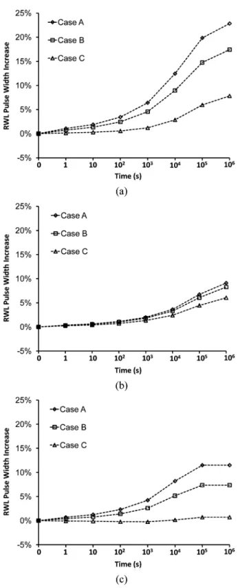
time. Fig. 11(a) shows that the RWL pulse width increases with usage (stress) time when both NBTI and PBTI are considered. The increase in Case A is the most serious. When only NBTI is considered, the RWL pulse width increases in all cases. How-ever, when only PBTI is considered, the RWL pulse width of Case C remains relatively unchanged. The width of RWL pulse is determined by the signal transferring delay of RWL logic path and the latency of the Read-Replica circuit. In Case A and B, the delay of the Read-Replica circuit increases significantly (Fig. 9), thus increasing the RWL pulse width. Although the delay of the Read-Replica circuit decreases slightly in Case C (Fig. 9), the RWL logic prefers to transfer logic “1,” leading to decrease of RWL truing-on delay (Fig. 7) and increase of RWL turning-off delay. Thus, the RWL pulse width also increases in Case C. Fig. 11(b) shows the degradation (increase) of RWL pulse width when only NBTI is considered. Fig. 11(c) shows the degradation of RWL pulse width when only PBTI is considered. The RWL pulse width degradation of Case C is the smallest comparing to that in Fig. 11(a) and (b) because of its smallest Read-Replica circuit delay [Fig. 9(c)].
The Read-Replica circuit turns off RWL and enables LRD and GRD to charge (precharge) the LRBL and GRBL to enter the Standby phase. If the SRAM operates at lower frequency, LRD and GRD would spend more time (and be stressed) under Standby condition, and the increase in Read access delay would be less. Fig. 12 compares Read access delay increase versus usage (stress) time for different LRBL length (from 16-bit/LRBL to 128-bit/LRBL) at 1 GHz (maximum frequency for 128-bit/LRBL) assuming the selected cell always transfers logic “0” to LRBL. The cases with shorter LRBL have faster Read/Write access and can operate at higher frequency. There-fore, when they all operate at 1.0 GHz, the cases with shorter LRBL would spend more time in Standby (Precharge) state, and their delay increases would be smaller.
B. Write Operation
When the SRAM is not performing Write operation, the precharge circuits in the Local Write Driver (LWD) keep the voltage level of Local WBL (LWBL) pair at VDD. During Write cycles, the timing control unit informs the decoder to turn off the precharge circuits in LWDs and enable LWDs and Global Write Drivers (GWDs) to transfer input data to LWBL pairs. The timing control unit also fires up the decoder to turn on the selected Write WL (WWL) and Dummy WWL (DWWL).
Fig. 11. Increase of RWL pulse width versus usage (stress) time: (a) with NBTI and PBTI; (b) with NBTI; (c) with PBTI.
After the state of the Write Monitor changes, WDone becomes logic “1.” The timing control circuit informs the decoder to turn off the selected WWL and DWWL, and the Write cycle completes.
Fig. 13(a) shows the combined impacts of NBTI and PBTI on the turning-on delays of WWL and DWWL. Similar to RWL and DRWL, the turning-on delay of WWL is smaller than
Fig. 12. Read access delay increase versus usage (stress) time for different LRBL length (GRBL length is 1024-bit) with NBTI and PBTI (SRAM oper-ates at 1.0 GHz, the maximum frequency for 128-bit/LRBL).
that of DWWL in the corresponding case. The reason is that the DWWL turns on every Write cycle, whereas a WWL only turns on when it is selected. Thus, WWL drivers and the cor-responding decoding path spend longer time in Standby mode and prefer to transfer logic “1,” and WWL turning-on delay decreases. The WWL (DWWL) turning-on delay for Case A is longer than Case B and Case C. This is because, for case A, the SRAM executes Write operation frequently, and all transistors in LWD and GWD become weaker, and the WWL (DWWL) turning-on delay degrades more. Fig. 13(b) and (c) show the changes of WWL and DWWL turning-on delays versus usage (stress) time with NBTI and PBTI, respectively. The impact of PBTI on WWL/DWWL turning-on delay degradation is more significant than NBTI because the drift induced by PBTI is larger than NBTI in our analysis model. Moreover, comparing Figs. 7 and 13, we can find the increase of RWL turning-on delay is more serious than that for WWL. This is because the WWL pulse width is smaller than the RWL pulse width in the subject SRAM, thus WWL would spend more time in Standby phase compared with RWL with the same Read/Write probability.
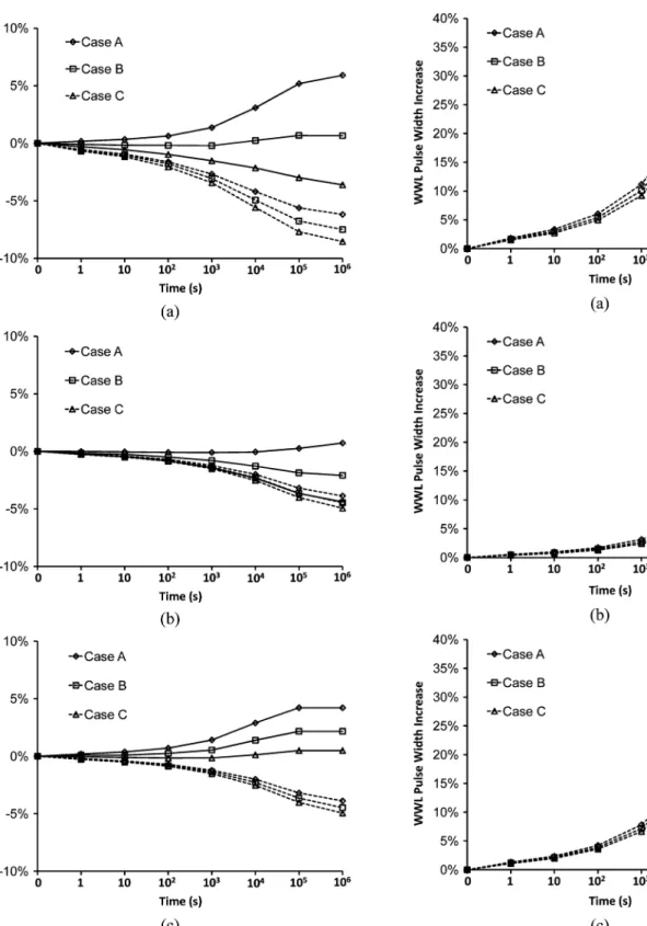
Fig. 14(a) shows that the WWL pulse width increases with usage (stress) time when both NBTI and PBTI are considered. The WWL pulse width increases in all cases. The Write-Replica circuit turns off the WWL once the state of the Write Monitor changes. The Write Monitor structure is shown in Fig. 15, and its basic structure is a two-port 8T SRAM cell. When the SRAM is not performing Write operation, , and node Q and QB store logic “1” and “0,” respectively. During Write cycle, DWWL turns on and the voltage level of DWBL is set to logic “0.” After the state of the Write Monitor changes, signal WDone becomes logic “1” and the Timing Control Unit turns off WWL and resets the Write Monitor. According to our WM analysis in Section III, WM is improved in most of the cases. Consequently, the Write time (Time-to-Write) of the Write Monitor cell should also be improved. However, due to the latency degradation of DWWL drivers and corresponding decoding logic path, the WWL width increases. As a result, the Write cycle time also
Fig. 13. Change of WWL turning-on delay versus usage (stress) time: (a) with NBTI and PBTI; (b) with NBTI; (c) with PBTI. A dashed line represents a normal WWL, and a solid line represents the DWWL.
increases. Note that the Write cycle time is still smaller than the Read cycle time in the subject SRAM design. Fig. 14(b) and (c) show the impact of NBTI and PBTI on WWL pulse width, respectively. The WWL pulse width degradation induced by PBTI is still more serious than that by NBTI.
Fig. 14. Increase of WWL pulse width versus usage (stress) time: (a) with NBTI and PBTI; (b) with NBTI; (c) with PBTI.
V. NBTI/PBTI TOLERANCETECHNIQUES
In previous sections, we analyzed impacts of NBTI and PBTI on 8T SRAM cell, Read operation, and Write operation. The degradation of decoding paths, RWL derivers, and WWL drivers can be mitigated by NBTI/PBTI-aware transistor sizing.
Fig. 15. Write Monitor structure.
However, transistor sizing is not applicable to mitigate the re-liability and performance degradation of a bit-cell due to hard area constraint. In this section, we focus on mitigating the long term degradation of cell array.
A. Write Half-Select SNM Improvement
When an 8T SRAM cell is under NBTI and PBTI stress, its stability degrades due to drifts of NFET and PFET pairs. The WWL pulse width also increases with usage (stress) time, leading to more serious Write Half-Select disturb. Thus, after long time of usage, data violation may happen.
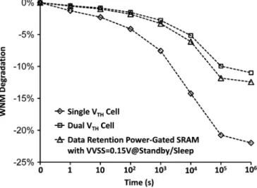
To mitigate long-term Half-Select stability degradation, we can use a dual 8T SRAM cell. The PFET loading tran-sistor pair (ML1 and ML2 in Fig. 3), NFET driving trantran-sistor pair (MD1 and MD2), and NFET access transistors (MA1 and MA2) are high- devices. The mismatch induced by NBTI and BPTI reduces because high- devices have lower drift, resulting in less Write Half-Select SNM (HS-SNM) degradation. It is not suitable to assign the NFET stacked Read Buffer (MR1 and MR2) as high- devices due to Read performance consideration. Write delay (Time-to-Write) of a dual- 8T SRAM cell is slightly longer. However, the performance of the subject SRAM is limited by Read opera-tion, and the increase in Write delay does not degrade SRAM performance. Moreover, data-retention power-gating structure can also be used to mitigate the long-term stability degradation [8]. Fig. 16 shows an example of a SRAM array bank with a data-retention power-gating footer. MF1 is the power-switch for leakage reduction, and MF2 is the virtual ground clamping device for data-retention in Standby/Sleep mode. When an SRAM bank is in Standby/Sleep mode, the power-switch turns off and the virtual ground can be biased at a proper voltage level by adjusting the gate voltage of the clamping device. The power switch turns on only when the bank is selected. The voltage across the cell array is less than VDD in Standby/Sleep mode, thus reducing the cell mismatch induced by NBTI/PBTI and improving the Write HS-SNM. Fig. 17 compares the Write HS-SNM degradation for a single- cell with regular , a dual- cell, and a regular cell with data-retention power-gating banking structure. The of a high-device is larger than a regular- device by about 150 mV,
Fig. 16. A SRAM array bank with data-retention power-gating structure.
Fig. 17. Write Half-Select SNM (HS-SNM) degradation of a single- cell, a dual- cell, and a single- cell with date-retention power-gating struc-ture versus usage (stress) time with NBTI and PBTI.
and the virtual ground of the data-retention power-gating banking SRAM array is biased at 150 mV. The degradation of Write HS-SNM in dual- cell and power-gated regular SRAM cell are smaller than the single- cell. The improvements are about 10% and 9% respectively. We can use distributed data-retention power-gating technique [28] to fur-ther mitigate the Write HS-SNM degradation. In this technique, each row has its own power-gating structure. This power-gating structure has improved Write HS-SNM degradation tolerance than the banking power-gating structure due to lower proba-bility of turning on power switches. However, its area overhead would increase significantly. Besides, when an SRAM bank is selected, power switch turns on to bias the virtual ground at zero. In general, with proper size design, the delay degradation of SRAM Read and Write performance is containable, but the wake-up transition latency should be considered [8], [28], [29]. In order to mitigate virtual ground (power) line bouncing and SRAM data violation, a larger size power-gated SRAM bank should allow longer wake-up transition time.
B. Read Degradation Mitigation
NBTI and PBTI degrade Read performance severely when SRAM frequently executes Read operations. The drift of the Read Buffer and sensing delay increase of LRD dominate Read performance degradation in a hierarchical RBL structure. To mitigate the PBTI impacts on Read Buffer, a column-based power-switch can be inserted between the Read Buffer virtual ground (RVVSS) and ground as shown in Fig. 18. When
Fig. 18. A column-based power-switch inserted between the Read Buffer vir-tual ground (RVVSS) and ground.
a bank is not performing Read operation, the power-switch bi-ases RVVSS to VDD. Thus, of MR2 is zero even if
, and MR2 is no longer stressed. When a column is selected during Read cycles, its corresponding power-switch should bias RVVSS to ground. Because the decoding path of RDSleep is shorter than that of the selected RWL, RDSleep is ready be-fore the selected RWL. Thus, the delay of the column-based power-switch has negligible effect on the Read delay with prop-erly sizing of the power-switch.
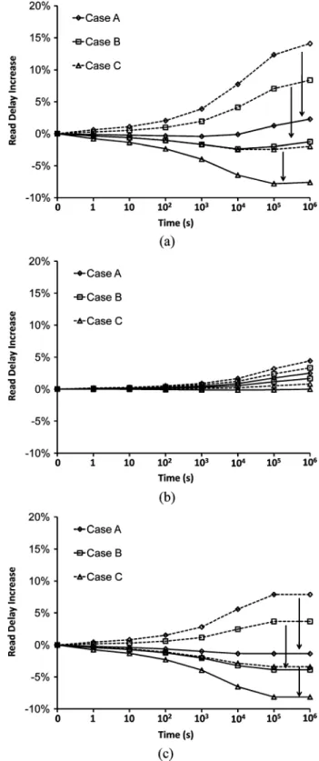
As discussed previously, the Read-Replica circuit dictates the Read performance as it is active every Read cycle, leading to degradation of DLRD, DRWL driver and corresponding decoding path. To reduce the activity of Read-Replica cir-cuit, each bank can have its own Read-Replica circuit. The area overhead of this structure is negligible because the local Read-Replica circuits can be formed by using those originally unused local columns under the DRGBL. Fig. 19(a) shows that the Read performance degradation due to NBTI/PBTI is mitigated by using multibank Read-Replica circuit structure and dynamic RVVSS biasing. The Read delay degradation is reduced (improved) by about 12% in Case A. Fig. 19(b) and (c) show, respectively, the case when only NBTI or only PBTI is present/considered. It can also been seen that the mitiga-tion/improvement becomes smaller when the Read probability decreases. Besides, the behavior of replica circuits become different form the normal access path after NBTI and PBTI stress because the activity property of replica circuits normally is higher than normal access path. By using multibank Read-and Write-Replica circuits, the behavior difference between replica circuits and normal access path can be mitigated. This is because the activity of local replica circuits more approach to the normal access path.
VI. CONCLUSION
This paper presents comprehensive analyses on impacts of NBTI and PBTI on the timing control of a two-port 8T SRAM with hierarchical bit-line structure based on PTM 32 nm high-k metal-gate technology models. We show that Read delay of a cell degraded and stability deteriorated after long time of
Fig. 19. Mitigation of Read delay degradation by using multibank Read-Replica circuit and dynamic RVVSS biasing: (a) with NBTI and PBTI; (b) with NBTI; (c) with PBTI. A dashed line represents the original structure. A solid line represents the multibank Read-Replica circuit structure with dynamic RVVSS biasing.
usage. However, WM could improve or degrade depending on the signal (stress) probability. We also show that replica circuits behave differently from normal access path after stress. The degradation of Read-Replica timing control circuit is shown to dictate the Read performance as it would be active in every single Read cycle. The WWL pulse width increases with
difference between replica circuits and normal access paths can also be improved by using multibank Read- and Write-Replica circuit.
REFERENCES
[1] S. Zafar et al., “A comparative study of NBTI and PBTI (charge trap-ping) in SiO /HfO stacks with FUSI,TiN,Re gates,” in IEEE Symp.
VLSI Technol. Dig. Tech. Paper, 2006, pp. 23–25.
[2] S. Zafar, A. Kumar, E. Gusev, and E. Cartier, “Threshold voltage insta-biltes in high-k gate dielectric stacks,” Trans. Device Mater. Rel., vol. 5, no. 1, pp. 45–64, Mar. 2005.
[3] V. Gupa and M. Anis, “Statistical design of 6T SRAM bit cell,” IEEE
Trans Circuit Syst. I, Reg. Paper, vol. 57, no. 1, pp. 93–104, Jan. 2010.
[4] S. Mukhopadhyay, H. Mahmoodi, and K. Roy, “Modeling of failure probability and statiscal design of SRAM array for yield enhancement in nanoscaled CMOS,” IEEE Trans. Comput.-Aided Design Integr.
Circuit Syst., vol. 24, no. 12, pp. 1859–1880, Dec. 2005.
[5] K. Kang, H. Kufluoglu, K. Roy, and M. A. Alam, “Impact of negative-bias temperature instability in nanoscale SRAM array: Modeling and analysis,” IEEE Trans. Comput.-Aided Design Integr. Circuit Syst., vol. 26, no. 10, pp. 1770–1781, Oct. 2007.
[6] A. Bansal, R. Rao, J. J. Kim, S. Zafar, J. H. Stathis, and C. T. Chuang, “Impact of NBTI and PBTI in SRAM bit-cells: Relative sensitivities and gudlines for applicarion-specific target stability/performance,” in
Proc. IEEE Int. Rel. Phys. Symp., 2009, pp. 745–749.
[7] A. Bansal, R. Rao, J. J. Kim, S. Zafar, J. H. Stathis, and C. T. Chuang, “Imapcts of NBTI and PBTI on SRAM static/dynamic noise margins and cell failure probability,” Mircroelectron. Rel., vol. 49, no. 6, pp. 642–649, Jun. 2009.
[8] H. I. Yang, W. Hwang, and C. T. Chuang, “Impacts of NBTI/PBTI and contact resistance on power-gated SRAM wih high-k metal-gate devices,” IEEE Trans. Very Large Scale Integr. (VLSI) Syst., accepted for publication.
[9] J. C. Lin, A. S. Oates, and C. H. Yu, “Time dependent degra-dation of SRAM fabricated with high-k gate dielectrics,” in Proc. IEEE
Int. Rel. Phys. Symp., 2007, pp. 439–444.
[10] H. Nho, S.-S. Yoon, S. S. Wong, and S.-O. Jung, “Numerical estimation of yield in sub-100-nm SRAM design using Monte Carlo simulation,”
IEEE Trans Circuit Syst. II, Exp. Briefs, vol. 55, no. 9, pp. 907–911,
Sep. 2008.
[11] M.-F. Chang, S.-M. Yang, and K.-T. Chen, “Wide embedded asynchronous SRAM with dual-mode self-timed technique for dy-namic voltage system,” IEEE Trans Circuit Syst. I, Reg. Papers, vol. 56, no. 8, pp. 1657–1667, Aug. 2009.
[12] B. C. Paul, K. Kang, H. Kufluoglu, M. A. Alam, and K. Roy, “Negative bisa temperature instabilty: Estimation and design for improved relaib-lity of nanoscale circuit,” IEEE Trans. Comput.-Aided Design Integr.
Circuit Syst., vol. 26, no. 4, pp. 743–751, Apr. 2007.
[13] B. C. Paul, K. Kang, H. Kufluoglu, M. A. Alam, and K. Roy, “Impact of NBTI on the temporal performance degradation of digital circuits,”
IEEE Trans. Electron Device Lett., vol. 26, no. 8, pp. 560–562, Aug.
2005.
[14] R. Vattikonda, W. Wang, and Y. Cao, “Modeling and minimization of PMOS NBTI effect for robust nanometer design,” in Proc. IEEE
Design Autom. Conf., 2006, pp. 1047–1052.
[15] W. Wang, S. Yang, S. Bhardwaj, R. Vattikonda, S. Vrudgula, F. Liu, and Y. Cao, “The impact of NBTI on performance of combinational and sequential circuits,” in Proc. IEEE Design Autom. Conf., 2006, pp. 364–369.
[19] [Online]. Available: http://www.eas.asu.edu/~ptm
[20] M. A. Alam, H. Kufluoglu, D. Varghese, and S. Mahapatra, “A com-prehansive model for PMOS NBTI degradation: Recent progress,”
Mi-croelectron. Rel., vol. 47, pp. 853–862, 2007.
[21] W. Wang, V. Reddy, A. T. Krishnan, R. Vattikonda, S. Vrudhula, and T. Cao, “Compact modeling and simulation of circuit relabilit for 65-nm CMOS technology,” Trans. Device Mater. Rel., vol. 7, no. 4, Dec. 2007. [22] S. Bhardwaj, W. Wang, R. Vattikonda, Y. Cao, and S. Vrudhula, “Pre-dictive modeling of the NBTI effect for reliable design,” in Proc. IEEE
Custom Integr. Circuits Conf., 2006, pp. 189–192.
[23] A. Bansal, R. Rao, J.-J. Kim, S. Zafar, J. H. Stathis, and C.-T. Chuang, “Impacts of NBTI and PBTI on SRAM static/dynamic noise margins and cell failure probability,” Microelectron. Rel., vol. 49, pp. 642–649, 2009.
[24] R. Fernandez, B. Kaczer, A. Nackaerts, S. Demuynck, R. Rodriguez, M. Nafría, and G. Groeseneken, “AC NBTI studied in the 1 Hz–2 GHz range on dedicated on-chip CMOS circuits,” in Proc. IEEE Int.
Elec-tron Devices Meet., Dec. 2006, pp. 1–4.
[25] [Online]. Available: http://www.itrs.net/
[26] C. T. Chuang, S. Mukhopadhyay, J. J. Kim, K. Kim, and R. Rao, “High-performance SRAM in nanoscale CMOS: Design challenges and tech-niques,” in Proc. IEEE Int. Workshop Memory Technol., Design, Test., 2009, pp. 4–11.
[27] T. Suzuki, Y. Yamagami, I. Hatanaka, A. Shibayama, H. Akamatsu, and H. Yamauchi, “A sub-0.5-V operating embedded SRAM featuring a multi-bit-error-immune hidden-ECC scheme,” IEEE J. Solid-State
Circuits, vol. 41, no. 1, pp. 152–160, Jan. 2006.
[28] C. H. Hua, T. S. Cheng, and W. Hwang, “Distributed data-rentention power gating techniques for column and row co-controlled embedded SRAM,” in Proc. IEEE Int. Workshop Memory Technol., Design, Test., 2005, pp. 129–134.
[29] H. I. Yang, M. H. Chang, T. J. Lin, S. H. Ou, S. S. Deng, C. W. Liu, and W. Hwang, “A controllable low-power dual-port embedded SRAM for DSP processor,” in Proc. IEEE Int. Workshop Memory Technol.,
Design, Test., Dec. 2007, pp. 27–30.
Hao-I Yang (S’09) received the B.S. and M.S. de-grees in electrical engineering from National Cheng Kung University, Tainan, Taiwan, in 2003 and 2005, respectively. He is working toward the Ph.D. degree in electronic engineering from National Chiao Tung University, Hsinchu, Taiwan.
Shyh-Chyi Yang was born in Taipei, Taiwan, in 1985. He received the B.S. degree in the electrical engineering from National Chung Hsing University, Taichung, Taiwan, in 2007 and the M.S. degree in electrical engineering from Nation Chiao Tung University, Hsinchu, Taiwan, in 2009.
In 2010, he joined MStar semiconductor, Inc., Hsinchu. He currently works on the research and development of DTV system. His interests include high performance circuit design and ultralow-voltage SRAM design.
Wei Hwang (F’01-LF’09) received the B.Sc. degree from National Cheng Kung University, Tainan, Taiwan, the M.Sc. degree from National Chiao Tung University, Hsinchu, Taiwan, and the M.Sc. and Ph.D. degrees in electrical engineering from the University of Manitoba, Winnipeg, MB, Canada, in 1970 and 1974, respectively.
From 1975 to 1978, he was an Assistant Professor with the Department of Electrical Engineering, Con-cordia University, Montreal, QC, Canada. From 1979 to 1984, he was an Associate Professor with the De-partment of Electrical Engineering, Columbia University, New York. From 1984 to 2002, he was a Research Staff Member with the IBM Thomas J. Watson Re-search Center, Yorktown Heights, NY, where he worked on high performance DRAM and microprocessor design. In 2002, he joined the National Chiao Tung University (NCTU), Hsinchu, Taiwan, as the Director of Microelectronics and Information Systems Research Center until 2008. Currently, he is a Chair Pro-fessor with the Department of Electronics Engineering, where he is engaging in teaching and research on low power memories and microsystems. During 2003–2007, he served as Co-Principal Investigator of the National System-on-Chip (NSoC) Program in Taiwan. From 2005 to 2007, he also served as a Senior Vice President and Acting President of NCTU, respectively. He is the coauthor of the book Electrical Transports in Solids-With Particular Reference to
Or-ganic Semiconductors (Pergamon Press, 1981), which has been translated into
Russian and Chinese. He has authored or coauthored more than 200 technical papers in renowned international journals and conferences, and holds over 170 international patents (including 66 U.S. patents).
Prof. Hwang was a recipient of several IBM Awards, including 16 IBM In-vention Plateau InIn-vention Achievement Awards, four IBM Research Division Technical Awards, and the CIEE Outstanding Electrical Engineering Professor Award in 2004 and Outstanding Scholar Award from the Foundation for the Advancement of Outstanding Scholarship for 2005 to 2010. He was named an IBM Master Inventor. He was President, Board Director, and Chairman of the Boards of Directors of the Chinese American Academic and Professional So-ciety (CAAPS) from 1986 to 1999. He is a member of the New York Academy of Science, Sigma Xi, and Phi Tau Phi Society. He has served several times in the Technical Program Committee of the ISLPED, SOCC, A-SSCC. He served as the General Chair of 2007 IEEE SoC Conference (SOCC 2007) and the General Chair of 2007 IEEE International Workshop on Memory Technology, Design, and Testing (MTDT 2007). Currently, he is serving as Founding Director of Center for Advanced Information Systems and Electronics Research (CAISER) of University System of Taiwan, UST, and Director of ITRI and NCTU Joint Research Center. He is also serving as a Supervisor of IEEE Taipei Section.
Ching-Te Chuang (S’78-M’82-SM’91-F’94) re-ceived the B.S.E.E. degree from National Taiwan University, Taipei, Taiwan in 1975 and the Ph.D. degree in electrical engineering from University of California, Berkeley, in 1982.
From 1977 to 1982 he was a Research Assistant in the Electronics Research Laboratory, University of California, Berkeley, working on bulk and surface acoustic wave devices. He joined the IBM T. J. Watson Research Center, Yorktown Heights, NY, in 1982. From 1982 to 1986, he worked on scaled bipolar devices, technology, and circuits. He studied the scaling properties of epitaxial Schottky barrier diodes, did pioneering works on the perimeter effects of advanced double-poly self-aligned bipolar transistors, and designed the first subnanosecond 5-Kb bipolar ECL SRAM. From 1986 to 1988, he was Manager of the Bipolar VLSI Design Group, working on low-power bipolar circuits, high-speed high-density bipolar SRAMs, multi-Gb/s fiber-optic data-link circuits, and scaling issues for bipolar/BiCMOS devices and circuits. Since 1988, he has managed the High Performance Circuit Group, investigating high-performance logic and memory circuits. Since 1993, his group has been primarily responsible for the circuit design of IBM’s high-performance CMOS microprocessors for enterprise servers, PowerPC workstations, and game/media processors. Since 1996, he has been leading the efforts in evalu-ating and exploring scaled/emerging technologies, such as PD/SOI, UTB/SOI, strained-Si devices, hybrid orientation technology, and multigate/FinFET devices, for high-performance logic and SRAM applications. Since 1998, he has been responsible for the Research VLSI Technology Circuit Co-design strategy and execution. He took early retirement from IBM to join National Chiao-Tung University, Hsinchu, Taiwan, as a Chair Professor in the Depart-ment of Electronics Engineering in February 2008. His group has also been very active and visible in leakage/variation/degradation tolerant circuit and SRAM design techniques. He holds 31 U.S. patents with another 14 pending. He has authored or coauthored more than 290 papers, including many invited papers in international journals such as the International Journal of High
Speed Electronics, PROCEEDINGS OF THEIEEE, IEEE Circuits and Devices
Magazine, and Microelectronics Journal. He has presented numerous plenary,
invited or tutorial papers/talks at international conferences such as International SOI Conference, DAC, VLSI-TSA, ISSCC Microprocessor Design Workshop, VLSI Circuit Symposium Short Course, ISQED, ICCAD, APMC, VLSI-DAT, ISCAS, MTDT, WSEAS, VLSI Design/CAD Symposium, and International Variability Characterization Workshop.
Dr. Chuang has received 1 Outstanding Technical Achievement Award, 1 Re-search Division Outstanding Contribution Award, 5 ReRe-search Division Awards, and 12 Invention Achievement Awards from IBM. He has also received the Outstanding Scholar Award from Taiwan’s Foundation for the Advancement of Outstanding Scholarship for 2008 to 2013. He served on the Device Tech-nology Program Committee for IEDM in 1986 and 1987, and the Program Com-mittee for Symposium on VLSI Circuits from 1992 to 2006. He was the Publica-tion/Publicity Chairman for Symposium on VLSI Technology and Symposium on VLSI Circuits in 1993 and 1994, and the Best Student Paper Award Subcom-mittee Chairman for Symposium on VLSI Circuits from 2004 to 2006. He was the Corecipient of the Best Paper Award at the 2000 IEEE International SOI Conference.
![Fig. 2. drifts induced by NBTI and PBTI using RD framework cali- cali-brated with published data [1], [2]](https://thumb-ap.123doks.com/thumbv2/9libinfo/7645941.138825/3.888.61.831.96.374/drifts-induced-nbti-pbti-using-framework-brated-published.webp)