Effect of thermal treatment on physical, electrical properties and reliability of
porogen-containing and porogen-free ultralow-k dielectrics
Yu-Min Chang
a, Wei-Yuan Chang
b, Jun-Fu Huang
b, Jihperng Leu
a, Yi-Lung Cheng
b,⁎
a
Department of Material Science and Engineering, National Chiao-Tung University, Shin-Chu, Taiwan, ROC
bDepartment of Electrical Engineering, National Chi-Nan University, Nan-Tou, Taiwan, ROC
a b s t r a c t
a r t i c l e i n f o
Available online 6 November 2012 Keywords: Low-k dielectric Porogen UV curing Reliability Breakdown TDDB
The effects of thermal annealing on the physical, electrical properties and reliability of porogen-containing and porogen-free ultralow-k dielectrics prepared by plasma-enhanced chemical vapor deposition (PECVD) are inves-tigated. The porogen-free low-k dielectrics are obtained by using UV curing process to removal organic sacrificial phase and to generate open porosity. The results are compared with PECVD porogen-containing low-kfilms fab-ricated without UV curing process and PECVD low-k dielectrics deposited without organic sacrificial phase. The experimental results show that all low-kfilms remained stable after they were experimentally heating to tem-peratures up to 700 °C. The non-porous low-kfilms also showed the highest reliability. Although the porous-free low-kfilm requires an additional UV curing process, the heat stress confirmed that its thermal stability was better than that of the porogen-containing low-kfilm. At an annealing temperature above 500 °C, the heating process is comparable to UV curing, but does not provide Si\O\Si cross-linking within the film. At an annealing of 600 °C, the porogen-free low-kfilms have a relatively higher breakdown electric-field and longer failure time in comparison to the porogen-containing low-kfilms. However, pores generated in porogen-containing low-kfilms at high temperature cause reliability to degrade with annealing temperature.
Crown Copyright © 2012 Published by Elsevier B.V. All rights reserved.
1. Introduction
Advanced Cu/low-k integration interconnects the use of porous organosilica low-k materials with k-values between 2.4 and 3.0 to re-duce signal propagation delay, cross-talk, and power consumption in integrated circuit[1–3]. A major strategy for decreasing the k-value of dielectricfilms is introducing the material porosity [4,5]. Recently, microelectronic applications of PECVD low-kfilms have increased due to their simplicity and compatibility with technology require-ments[6]. Porosity is introduced into PECVD low-k dielectric mainly by using sacrificial porogens[7], which are cyclic hydrocarbons that can be removed by UV-assisted-thermal curing[8]. The porogen mol-ecules are photodissociated by UV light with the formation of volatile hydrocarbons and nonvolatile carbon-rich porogen residues[9].
During the interconnect fabrication process and IC packaging step, thermal annealing process is the indispensable step[10–12]. Addition-ally, annealing of lower level interconnects is performed many times higher than those for annealing of upper level interconnects when fab-ricating multilevel interconnects. Therefore, the effects of thermal annealing process on thefilm properties of porous low-k materials should be addressed. Moreover, the effects of thermal annealing on the interconnect performance, particularly reliability, must also be con-sidered. Consequently, the main purpose of this work is to clarify the
stability of various low-k materials, including non-porous and porous materials, when exposed to heat stress. Basicfilm properties, porosity, mechanical, and electrical performance were performed to clarify how thermal stress affects the chemical structure of dielectricfilms. Finally, the intrinsic reliability of TDDB results for the low-k dielectrics under the different thermal stresses was also investigated.
2. Experiments
All thinfilm depositions were performed on 300 mm p-type Si wafers by Applied Material PECVD reactor with a radio frequency (rf) of 13.56 MHz at a temperature of 300 °C. Three different low-k films with approximate thicknesses of 300 nm were obtained in this study. The porogen-containing low-k films were deposited from diethoxymethylsilane (DEMS) and alpha-terpiene (ATRP) as a matrix and porogen precursor, respectively. A small amount of oxygen was also introduced as an oxidant. To create the porogen-free low-k films, UV curing of the porogen-containing low-k films was per-formed to remove the organic porogen for 10 min. The low-kfilms deposited without organic porogen content (briefly call “low-k with-out porogen) were also prepared in the same system as a reference. All low-k films were thermally annealed at varying temperatures (400–900 °C) in ambient N2for 1 min.
The thickness and refractive index (RI, at 633 nm) of the as-deposited films were analyzed with an ellipsometer in an optical-probe system. The film thickness shrinkage ratio was calculated as the difference in the film ⁎ Corresponding author. Tel.: +886 49 2910960 4987; fax: +886 49 2917810.
E-mail address:[email protected](Y.-L. Cheng).
0040-6090/$– see front matter. Crown Copyright © 2012 Published by Elsevier B.V. All rights reserved.
http://dx.doi.org/10.1016/j.tsf.2012.09.088
Contents lists available atSciVerse ScienceDirect
Thin Solid Films
thickness before and after annealing process. Chemical bonding of the low-kfilms was characterized by Fourier transform infrared ab-sorption (FTIR). A water contact angle tool was used to determine the hydrophilic/hydrophobic properties of the surface. Ellipsometric porosimetry (EP) was used to assess the isotherm of ethanol adsorption and desorption to determine the total porosity and the pore size. The nano-hardness and modulus of low-kfilms were measured on an MTS Nano Indentor XP system. The sample thickness for nano-hardness measurements was approximately 0.6μm and the depth penetration was about 100 nm at down force of ~0.3 mN. The dielectric constant was obtained by measuring the capacitance–voltage using a mercury probe at 1 MHz. The metal–insulator–semiconductor (Al/low-k/Si; MIS) capacitors with p-type silicon (Si) as the substrates and aluminum (Al) as the metal electrodes were fabricated. The capacitors had an area of 30×30μm2. Negative voltages from 0 to 200 V were applied to the Al electrodes, and leakage–voltage (I–V) characteristics and dielectric breakdown electricfields were measured with a semiconductor analyzer (HP4286) at room temperature. Time-dependent dielectric breakdown (TDDB) measurements were performed on the same MIS capacitors. 3. Results and discussion
Fig. 1shows the varying thickness shrinkage ratios and refractive index obtained for different low-kfilms at varying annealing tempera-tures from 400 °C to 900 °C. At annealing temperature above 800 °C, thickness decreased and refractive index significantly increased in all low-kfilms, which indicated that the low-k films analyzed here are ther-mally stable up to 700 °C. The porogen-containing low-kfilms without UV curing showed the largest declines infilm thickness, especially at annealing temperatures above 500 °C. The reduced film thickness resulted mainly from the porogen decomposition, which implies that thermal treatment at an annealing temperature above 500 °C has a decomposing effect, similar to that of UV curing. The similar changes in the refractive index also demonstrate that the porogen materials in low-kfilms begin decomposing at annealing temperature above 500 °C. Compared to porogen-containing and porogen-free low-kfilms, the ex-periments showed that low-kfilms deposited without organic porogen content remain unchanged until the annealing temperature reaches 800 °C.
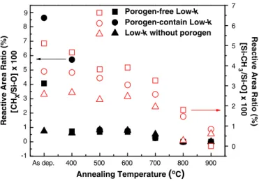
Fig. 2compares the FTIR spectrum of the as-deposited low-kfilms. The characteristic absorptions are: network Si\O\Si stretching (~1060 cm−1), cage-like Si\O\Si stretching (~1150 cm−1), Si\O\Si bending (~440 cm−1), Si\CH3 bending (~1270 cm−1), and C\Hx stretching (~2850–3100 cm−1). Thefigure shows that the
porogen-containing low-kfilm contains more C\Hxstretching bonding, which indicates that this bonding is caused mainly by molecular porogen. To examine the effect of annealing temperature on the change in bonding structures, the relative area ratio of Si\CH3and C\Hxbonds were ana-lyzed as a function of annealing temperature. The relative area ratios are calculated from the following wavenumber regions:
TheðSi\CH3=Si\OÞpeak ratio ¼ ð1250–1285cm−1Þ=ð950–1250cm−1Þ:
TheðC\Hx=Si\OÞpeak ratio ¼ ð2800–3050cm−1Þ=ð950–1250cm−1Þ: Fig. 3displays the analytical results. Comparison of the as-deposited low-kfilms shows that the low-k films deposited with organic porogen have higher ratios of Si\CH3and C\Hxbonds in comparison to those without organic porogen. After 500 °C annealing, the ratio of C\Hx bonding remains constant for all three low-kfilms. These experimental results also confirm that molecular porogen can be completely removed by annealing at a temperature above 500 °C. Analysis of Si\CH3 bond-ing ratio shows that the porogen-free low-kfilm contains more Si\CH3 bonds, which suggests that Si\CH3bonding can be created by UV irra-diation. The same phenomenon was reported earlier in Choi et al.[10]. Additionally, Si\CH3bonding slightly declines at an annealing temper-ature of 700 °C and is completely eliminated at an annealing tempera-ture of 900 °C. Further analysis of the\OH stretching mode in the
0.6 0.8 1.0 1.2 Thickness Shrinkage 900 500 400 As dep. 600 700 800 1.2 1.3 1.4 1.5 1.6 1.7 Reflection Index (633nm) Annealing Temperature
(
oC)
Porogen-free Low-k Porogen-contain Low-k Low-k without porogenFig. 1. Thickness shrinkage and refractive index as functions of annealing temperature for
various low-kfilms. 1000 1500 2000 2500 3000 3500 4000 0.4 0.6 0.8 1.0 1.2
Porogen-free Low-k
Porogen-contain Low-k
Low-k without porogen
Absorbance (Arb.Unit)
Wavenumber (cm-1)
Fig. 2. FTIR spectra of as-deposited low-kfilms.
-1 0 1 2 3 4 5 6 7 8 9 Reac ti ve Area Ra ti o (% ) [CH X /S i-O ]] x1 0 0 Annealing Temperature
(
oC)
900 500 400 As dep. 600 700 800 0 1 2 3 4 5 6 7 R e a ct ive A re aR a tio (% ) [S i-C H 3 /S i-O ]] x 10 0 Porogen-free Low-k Porogen-contain Low-k Low-k without porogenFig. 3. FTIR ratios of Si\CH3/Si\O and C\Hx/Si\O bonds as functions of annealing
3400 cm−1region of the FTIR spectrum for all low-kfilms at thermal annealing temperature above 700 °C showed that \OH stretching mode correlates with annealing temperature. The formation of the \OH stretching mode can be explained as follows: Si\CH3 bonds break to form Si· center dangling defect under thermal annealing at a temperature above 700 °C. These broken bonds can easily interact with OH/H2O,
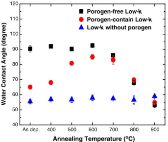
To understand the effect of annealing temperature on the hydrophilicity/hydrophobicity of the low-k films, water contact angle (WCA) was measured on the film surfaces. It is reported that the surfaces remained hydrophobic as WCA was higher than 85 °C[11].Fig. 4 presents the WCA plot as a function of annealing temperature for various low-kfilms. Interestingly, comparison of three different low-kfilms shows that the porogen-free low-k film has the highest WCA, which indicates that thisfilm is the most hydrophobic, possibly because the high ratio of Si\CH3bonds decreases the polarity required for the hydrophobic properties to the low-k material. The WCA is lowest in the low-kfilms deposited without porogen and its dependence on the annealing temperature is negligible, which suggests that the thermal annealing process does not change surface polarity. In the porogen-containing low-kfilms, WCA significantly increases when annealing temperature exceeds 500 °C, indicating that the porogen low-kfilms become more hydrophobic as the porogen was removed to form pores. This experimental result also implies that the internal pore surfaces of thefilms are hydrophobic. At annealing temperatures above 700 °C, WCA begins to decline in both low-k films deposited with porogen due to the formation of\OH bonds.
Fig. 5(a) and (b) shows the hardness (H) and elastic modulus (E), re-spectively, as functions of annealing temperature for the various low-k films. To avoid the substrate effect on the low-k films, the films with thicknesses greater than 600 nm was used for the nanoindentation mea-surements. The order of the as-deposited low-kfilms in terms of hardness and elastic modulus was: low-kfilms without porogen>porogen-free low-kfilms>porogen-containing low-k films. This order indicates that porogen degrades mechanical strength in the low-kfilm as reported in the literature[13]. Additionally, the UV curing process strengthensfilm bonding in porogen low-kfilms. Regarding the annealing temperature effect, annealing temperatures below 600 °C do not affect low-kfilms without organic porogen content. However, the mechanical strength of porogen-free and porogen-containing low-k films slightly decreases with annealing temperature, which indicates that thermal annealing alters the microstructure of porogen low-kfilms. Additionally, at an-nealing temperatures exceeding 700 °C, the elastic modulus and hard-ness begin to increase substantially in all low-kfilms. This improvement
is attributable to changes in the bonding structure of the low-kfilms. FTIR analysis also shows that breaking the terminal Si\CH3and Si\H bonds in the low-k films causes formation of new Si\O\Si cross-linking bonds, which increases mechanical strength.
Table 1presents the measured dielectric constant, pore size, and po-rosity of various low-k dielectrics at annealing temperatures of 400 °C and 600 °C. The data show that the porosity of the low-kfilm deposited without organic sacrificial phase approaches zero after the annealing pro-cess, which is consistent with the results of the thickness shrinkage and FTIR. This indicates that the low-kfilm deposited without organic sacrifi-cial phase is thermally stable. In the porogen-free and porogen-containing low-kfilms without thermal annealing, the porosity of the porogen-free low-kfilm is about two-fold higher than that of the porogen-containing low-kfilm, which indicates that UV curing removes the organic sacrificial phase to produce pores in the low-kfilms. In the porogen-free low-k films, the porosity was unrelated to annealing temperature. In contrast, the porosity of the porogen-containing low-k film slightly increases after 400 °C annealing and significantly increases after 600 °C annealing. In low-k dielectrics annealed at 600 °C, the porosity of the porogen-containing low-kfilm is about 6% higher than that of the porogen-free 40 50 60 70 80 90 100 110 120
Water Contact Angle (degree)
Annealing Temperature (oC) 900 500 400 As dep. 600 700 800 Porogen-free Low-k Porogen-contain Low-k Low-k without porogen
Fig. 4. Water contact angle value as functions of annealing temperature for various low-k films.
(a)
(b)
0 10 20 30 40 50 180 200Elastic Modulus (GPa)
Annealing Temperature (oC) 900 500 400 As dep. 600 700 800 0 1 2 3 11 12 13 14 Hardness (GPa) Annealing Temperature (oC)
Porogen-free Low-k
Porogen-contain Low-k
Low-k without porogen
Porogen-free Low-k
Porogen-contain Low-k
Low-k without porogen
900 500
400
Asdep. 600 700 800
Fig. 5. (a) Hardness values as functions of annealing temperature and (b) elastic modulus as
low-kfilm, which suggests that the porogen-free low-k film with UV cur-ing strengthens some unstable bonds, which leads to a reduced porosity. Fig. 6shows the measured k-values of various low-kfilms at 1 MHz. The k-value of the as-deposited porogen-containing low-k films is approximately 2.9 due to their low open porosity. The UV curing re-duces the k-value of porogen-free low-kfilm to about 2.4 due to partial porogen removal, resulting in the increased porosity of thefilm. Analy-sis of the annealing temperature effect shows that all low-kfilms sig-nificantly degrade at annealing temperature above 800 °C, which is consistent with the results of thickness shrinkage and FTIR. At annealing temperature below 800 °C, different low-k films display different temperature-dependence trends. In low-k films deposited without porogen, the values remain virtually unchanged. However, the k-values of low-k films deposited with porogen correlate negatively with annealing temperature. The decrease in the porogen-containing low-kfilms is larger than that in porogen-free low-k films. The decrease in the k value with the annealing temperature in the porogen-free low-k films suggests that UV curing did not completely remove molecular porogen and that the thermal process further decomposes the remaining porogen residues. This postulation is also supported by FTIR results, which show that the peak area of CHxbonding decreases with annealing temperature.
Fig. 7compares the I–V characteristics of MIS structures with differ-ent as-deposited low-k dielectrics. All low-kfilms show similar curves for leakage current density versus electrical-filed. The leakage current in-creases with the electricalfiled before reaching a plateau. Finally, the leakage current density abruptly increases. Interestingly, the low-k films deposited without porogen have a higher leakage current, but a higher dielectric breakdown electric-field in comparison to the low-k films deposited with porogen. In the low-k films deposited with porogen, leakage current densities are comparable, but the porogen-free low-k films have a lower dielectric breakdown electric-field. These comparison
results suggest that leakage current in low-kfilms seems to be impacted by the bonding structure and is not substantially impacted by porosity. However, porosity in the low-kfilm can affect dielectric breakdown strength.Fig. 8(a) and (b) compares the leakage current densities for electricalfields at 1 and 2 MV/cm and dielectric breakdown electric-field, respectively, as a function of annealing temperature. The leakage current densities significantly decrease with annealing process in the low-kfilms deposited without porogen, possibly due to moisture desorp-tion. However, the dielectric breakdown electric-field is unaffected. In the porogen-containing low-kfilms, pore formation at annealing tem-perature of 600 °C slightly increases leakage current and substantially degrades the dielectric breakdown electric-field.
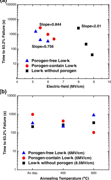
Time-dependence-dielectric-breakdown (TDDB) was also evaluated for various low-k dielectrics.Fig. 9(a) shows the failure time of the as-deposited low-kfilms versus electrical field for three different low-k dielectrics. This reliability assessment result shows a similar trend of degrading electrical properties in the low-k films deposited with porogen. Moreover, the porogen-free low-kfilms have a loner break-down failure time compared to the porogen-containing low-kfilms. Fig. 9(b) compares the failure time at 63.2% failure rate with annealing temperature for three different low-kfilms. The electrical filed was in-creased (8.5 MV/cm) to stress the low-k films deposited without porogen in order to shorten the testing time. In the low-kfilms deposit-ed without porogen, the failure times at a 63.2% failure rate are indepen-dent of annealing temperature, as observed in analyses of the dielectric breakdown electric-field. In the case of the low-k films deposited with porogen, annealing temperature affected dielectric breakdown failure time. However, the porogen-free and porogen-containing low-kfilms have a different temperature-dependence trend. In the porogen-containing low-kfilms, dielectric breakdown failure time correlates neg-atively with annealing temperature. In contrast, the dielectric break-down failure time in the porogen-free low-kfilms increases when the Table 1
Dielectric constant, porosity, and pore size for three different low-kfilms under various annealing temperatures.
Sample As-deposited 400 °C annealed 600 °C annealed
Dielectric constant (k) Porosity (%) Pore size (nm) Dielectric constant (k) Porosity (%) Pore size (nm) Dielectric constant (k) Porosity (%) Pore size (nm) Porogen-free low-k 2.42 13.4 1.35 2.36 14.1 1.35 2.05 15.3 1.7 Porogen-containing low-k 2.93 4.8 N/D 2.72 5.6 N/D 2.03 21.5 1.7
Low-k without porogen 3.0 N/D N/D 2.9 N/D N/D 2.93 N/D N/D
N/D = not detected. 1 2 3 6 8 10 12 900 500 400 Dielectric Constant Annealing Temperature (oC) As dep. 600 700 800
Porogen-free Low-k
Porogen-contain Low-k
Low-k without porogen
Fig. 6. Dielectric constants as functions of annealing temperature for various low-kfilms.
0 2 4 6 8 10 12 1E-10 1E-9 1E-8 1E-7 1E-6 1E-5 1E-4 1E-3 0.01 0.1
Leakage Current Density (A/cm
2)
Electric-field (MV/cm)
Porogen-free Low-k
Porogen-contain Low-k
Low-k without porogen
annealing process is performed at 600 °C. This improvement is attribut-able to removal of porogen residues by high temperature annealing. The remaining porogen residues in the low-kfilm apparently degraded elec-trical performance and reliability[14].
4. Conclusions
This paper investigated the resistance of various low-kfilms against heat stress. All low-kfilms in this study were shown to be thermally stable after they were experimentally heating up to 700 °C. Additionally, non-porous low-kfilms also showed the highest reliability. Although the porous-free low-kfilm requires an additional UV curing process, the heat stress confirmed that its thermal stability was better than that of the porogen-containing low-k film. At an annealing temperature above 500 °C, the heating process is comparable to UV curing, but does not pro-vide Si\O\Si cross-linking within the film. At an annealing of 600 °C, the porogen-free low-kfilms have a relatively higher breakdown electric-field and longer failure time in comparison to the porogen-containing low-k films. However, pores generated in porogen-containing low-k films at high temperature cause reliability to degrade with annealing temperature.
References
[1] A. Grill, Ann. Rev. Mater. Res. 39 (2009) 49.
[2] K. Maex, M.R. Baklanov, D. Shamiryan, F. Lacopi, S.H. Brongersma, Z.S. Yanovitskaya, J. Appl. Phys. 93 (2003) 8793.
[3] T. Furusawa, D. Ryuzaki, R. Yoneyama, Y. Homma, K. Hinode, J. Electrochem. Soc. 148 (2001) F175.
[4] A. Zenasni, B. Remiat, C. Waldfried, C.L. Cornec, V. Jousseaume, G. Passemard, Thin Solid Films 516 (2008) 1097.
[5] V. Jousseaume, O. Gourhant, P. Gonon, a. Zenasni, L. Favennec, J. Electrochem. Soc. 159 (2012) G249.
[6] F. lacopi, Y. Travaly, B. Eyckens, C. Waldfried, T. Abell, E.P. Guyer, J. Appl. Phys. 99 (2006) 053511.
[7] V. Jousseaume, A. Zenasni, L. Favennec, G. Gerbaud, M. Bardet, J.P. Simon, A. Humberte, J. Electrochem. Soc. 154 (2007) G103.
[8] A. Grill, V. Patel, J. Appl. Phys. 104 (2008) 024113. [9] Y.W. Li, C.F. Chen, Jpn. J. Appl. Phys. 41 (2002) 5734.
[10] C.K. Choi, C.Y. Kim, R. Navamathavan, H.S. Lee, J.K. Woo, M.T. Hyun, H.J. Lee, W.Y. Jeung, Curr. Appl. Phys. 5 (2011) S109.
[11] A.M. Urbanowicz, K. Vanstreels, P. Verdonck, E.V. Besien, T. Christos, D. Shamiryan, S.D. Gendt, M.R. Baklanov, J. Vac. Sci. Technol. B29 (2011) 032201-1.
[12] E. Hong, S. Demuynck, Q.T. Le, M. Baklanov, L. Carbonell, M.V. Hove, M. Meynen, Microelectron. Eng. 84 (2007) 2582.
[13] C.H. Huang, N.F. Wang, Y.Z. Tsai, C.I. Hung, M.P. Houng, Microelectron. Eng. 87 (2010) 1735.
[14] M.R. Baklanov, L. Zhao, E.V. Besien, M. Pantouvaki, Microelectron. Eng. 88 (2011) 990.
(a)
1E-10 1E-9 1E-8 1E-7 1E-6 1E-5Current Denstiy (A/cm
2) Annealing Temperature (oC) As dep. 400 600 Solid: 1MV/cm Hollow: 2MV/cm
(b)
1 2 3 4 5 6 7 8 9 10 11 12 13 14 600 400 Breakdwon Electric-field (MV/cm) Annealing Temperature (oC) As dep. Porogen-free Low-k Porogen-contain Low-k Low-k without porogenPorogen-free Low-k Porogen-contain Low-k Low-k without porogen
Fig. 8. (a) Leakage current density at 1 MV/cm and 2 MV/cm and (b) dielectric breakdown electric-field as functions of annealing temperature for various low-k films.
(a)
(b)
4 5 6 7 8 9 10 1 10 100 1000 10000 100000Porogen-free Low-k
Porogen-contain Low-k
Low-k without porogen
Slope=0.756 Slope=0.844 Time to 63.2% Failure (s) Electric-field (MV/cm) Slope=2.01 As dep. 400 600 1 10 100 1000 10000Porogen-free Low-k
(6MV/cm)Porogen-contain Low-k
(6MV/cm)Low-k without porogen
(8.5MV/cm)Time to 63.2% Failure (s)
Annealing Temperature (oC)
Fig. 9. (a) Time to dielectric breakdown at 63.2% failure as functions of stress electric-field for as-deposited low-kfilms and (b) time to dielectric breakdown t 63.2% failure as functions of