Investigation and Comparison of the GaN-Based
Light-Emitting Diodes Grown on High Aspect Ratio
Nano-Cone and General Micro-Cone Patterned
Sapphire Substrate
Jhih-Kai Huang, Da-Wei Lin, Min-Hsiung Shih, Member, IEEE, Member, Kang-Yuan Lee, Jyun-Rong Chen,
Hung-Weng Huang, Shou-Yi Kuo, Chung-Hsiang Lin, Po-Tsung Lee, Member, IEEE, Gou-Chung Chi, and
Hao-Chung Kuo, Senior Member, IEEE
Abstract—In this paper, we demonstrated the high
perfor-mance GaN-based LEDs by using a high aspect ratio cone-shape
nano-patterned sapphire substrate (HAR-NPSS). We utilized
nano-imprint lithography (NIL) and dry-etching system to
fabri-cate a high depth HAR-NPSS. The micro-scale patterned sapphire
substrate (PSS) was also used for comparison. A great
enhance-ment of light output was observed when GaN-based LEDs were
grown on a HAR-NPSS or a PSS. The light output power of
LEDs with a HAR-NPSS and LEDs with a PSS were enhanced
of 49 and 38% compared to LEDs with a unpatterned sapphire
substrate. The high output power of the LED with a HAR-NPSS
indicated that the technology of NAR-NPSS not only can improve
the crystalline quality of GaN-based LEDs but also a promising
development to a NPSS.
Index Terms—GaN, light-emitting diodes (LEDs), nano-imprint
lithography (NIL), nano-patterned sapphire substrate (NPSS).
I. I
NTRODUCTIONT
HE GaN-based LEDs have been widely used for light
source, backlight in liquid crystal displays, and solid state
lighting [1], [2] and became popular in the study. GaN is a very
hard and mechanically stable material. However, there is
actu-ally few suitable substrate can be used to grow GaN because
of the specific hexagonal lattice. Considering the high quality,
high throughput, low cost and mass production for GaN-based
Manuscript received December 01, 2012; revised April 16, 2013; accepted June 01, 2013. Date of publication June 25, 2013; date of current version November 13, 2013. This work was supported by the National Science Council, Republic of China, under NSC 100-3113-E-009-001-CC2
J.-K. Huang, D.-W. Lin, J.-R. Chen, H.-W. Huang, P.-T. Lee, G.-C. Chi, and H.-C. Kuo are with the Department of Photonics and Institute of Electro-Optical Engineering, National Chiao Tung University, Hsinchu 30010, Taiwan (e-mail: [email protected]).
M.-H. Shih is with the Department of Photonics and Institute of Electro-Op-tical Engineering, National Chiao Tung University, Hsinchu 30010, Taiwan, and also with the Research Center for Applied Sciences (RCAS), Academia Sinica, Taiwan (e-mail: [email protected]).
S.-Y. Kuo is with the Department of Electronic Engineering, Chang Gung University, TaoYuan 333, Taiwan.
K.-Y. Lee and C.-H. Lin are with the Luxtaltek Corporation, Miaoli 350, Taiwan.
Color versions of one or more of the figures are available online at http:// ieeexplore.ieee.org.
Digital Object Identifier 10.1109/JDT.2013.2270276
LEDs, sapphire substrates is a well known solution. Although
sapphire substrate is a very common substrate to GaN epitaxy,
the lattice mismatch between GaN and sapphire still limited the
light output and resulted in a low internal quantum efficiency
(IQE) and a poor external quantum effciency (EQE). The low
IQE is directly related to the threading dislocations (TDs)in the
GaN film. In order to decrease the TDs density and improve
the crystalline quality, a micro-scale patterned sapphire
sub-strate (PSS) is recommended to solve the problem [3], [4]. A
PSS served as a GaN template and the pattern could be
scat-tering centers for the guided light to improve GaN crystalline
quality and the light extraction efficiency. Recently, nano-scale
patterned sapphire substrate (NPSS) are investigated as a new
substrate to GaN-based LEDs. It was proposed that NPSS can
be a high potential template and provide a new type substrate
for GaN epitaxy [5]–[12]. The use of NPSS resulted in TDs
density reduction [9]–[11] and reduction in screw dislocation
density fraction [12] in GaN template. These reductions in both
dislocation density and screw dislocation density from the use
of NPSS resulted in improved IQE in InGaN QW LEDs
at-tributed to the reduced non-radiative recombination rate. In
ad-dition to the dislocation density reduction, several methods had
been pursued for achieving improved IQE in InGaN-based QW
LEDs by suppressing the charge separation in active regions
[13]–[18]. The charge separation suppression had been pursued
by using non/semi-polar QWs [13]–[15], and polar QWs with
large overlap designs [16]–[18]. The surface patterning based
on photonic crystals [19], [20] and self-assembled microlens
ar-rays [21], [22] had been reported for achieving large increase in
light extraction efficiency (LEE) in III-Nitride LEDs. Recently,
the effect of pattern density in PSS had been also shown to
af-fect the light extraction in GaN-based LEDs [23]. Although the
technology of NPSS has been reported to play an important role
for improving LEDs efficiency, there are few reports on the
rela-tion between the efficiency and the NPSS geometry. Due to the
hardness of sapphire, the etching depth is usually a bottleneck
to modify the profile for the dry-etching methods or wet-etching
methods for the NPSS patterns. The pattern profile is also a key
issue to the GaN quality when growing GaN layers on a
pat-terned substrate. In this study, the high aspect ratio cone-type
nano-patterned sapphire substrate (HAR-NPSS) was used to
de-crease the defect density and improve the quality of GaN LEDs.
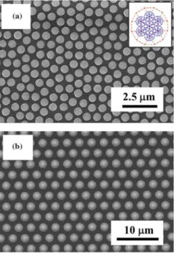
Fig. 1. (a) Schematic diagram of LED structure with a HAR-NPSS. (b) Cross-view SEM image of GaN/HAR-NPSS interface.
A nano-imprint lithography (NIL), which is a high throughput,
rapid and repeating process for mass production, was utilized to
fabricate a HAR-NPSS with a 12-fold a photonic quasi-crystal
(PQC) pattern [24]–[27].
II. E
XPERIMENTSFig. 1(a) shows the schematic diagram of the GaN-based
LEDs with a HAR-NPSS and Fig. 1(b) is the SEM cross-view
image around an interface of the GaN film and HAR-NPSS.
In order to fabricate a high depth HAR-NPSS, the NIL was
processed with a deep imprint-mold with a high depth of 700
nm. The following is the detail of the HAR-NPSS process flow
by using NIL and dry-etching system. First, an imprint-resist
was coated onto sapphire substrate surface. Then, a deep
pat-terned mold was placed onto sapphire substrate with an
im-print-resist film to transfer pattern by applying a high pressure
at a transition temperature. Second, the sapphire substrate and
the mold were cooled down to room temperature to release the
mold from the substrate. The thickness of the imprint-resist after
NIL process is approximately 800 nm. Finally, we used an
in-ductively coupled plasma reactive ion etching (ICP-RIE) with
the chemical mixture BCl Cl Ar of 50/20/5 sccm to transfer
the pattern onto sapphire substrate by a RF power of 450 W
and an ICP power of 200 W. The fabricated HAR-NPSS
sam-ples were patterned as a 12-fold PQC with a 450 nm diameter,
a 250 nm spacing distance and a 530 nm high etching depth.
The aspect ratio of HAR-NPSS is as high as 1.17 and the profile
of HAR-NPSS is cone-like type which is similar to the profile
of PSS. A sample with the PSS pattern and a flat sapphire
sub-strate were also prepared as the references in the experience.
The PSS was fabricated by the photo-lithography process. The
photo-resist AZ-5214-E was used as the etching mask and apply
the same ICP-RIE system to transfer pattern onto the sapphire.
The PSS pattern is with a diameter of 2 m, a spacing distance of
1 m and an etching depth of 1.3 m. The aspect ratio of PSS is
Fig. 2. (a) Top-view SEM image of a HAR-NPSS with a 12-fold PQC pattern. (b) Top-view SEM image of a PSS.
0.65. Fig. 2 shows the top-view images of the HAR-NPSS with
a 12-fold PQC pattern and PSS.
All LED structure were fabricated by the metal organic
chemical vapor deposition (MOCVD) system. The LED
struc-ture was described by following. The LED consists of a 50
nm-thick GaN nucleation layer grown at 500 C, a 3 m-thick
un-doped GaN (UN-GaN) buffer layer grown at 1050 C,
a 3 m-thick Si-doped GaN (N-GaN) layer grown at 1050
C, an unintentionally doped InGaN/GaN multiple quantum
well (MQW) active region grown at 770 C, a 50 nm-thick
Mg-doped p-AlGaN electron blocking layer grown at 1050 C,
and a 120 nm-thick Mg-doped p-GaN contact layer grown at
1050 C. The MQW active region consists of 14 periods of 3
nm/10 nm thick In
Ga
N/GaN quantum well layers and
barrier layers.
The LED devices were fabricated by standard LED chip
pro-cesses with a chip size of 575
250 m . A indium-tin-oxide
(ITO) thin film with a thickness of 240 nm is deposited onto
p-GaN surface. The n-contact and p-contact metal are Cr/Pt/Au
layers with thickness of 30/50/1400 nm.
III. R
ESULTS ANDD
ISCUSSIONThe transmission electron microscopy (TEM) images were
employed to investigate the crystalline quality of GaN layers
grown on a flat sapphire substrate, a PSS and a HAR-NPSS.
Fig. 3(a)–(c) show the TEM images of GaN-Based LEDs grown
on a flat sapphire, a PSS and a HAR-NPSS, respectively. It
can be seen that the TDs density of GaN epilayer were
drasti-cally reduced by using PSS and HAR-NPSS (Fig. 3(b) and (c))
as compared with GaN epilayer grown on a flat sapphire
sub-strate [Fig. 3(a)]. The reduction of TDs density for GaN epilayer
grown on PSS can be attributed to epitaxial lateral overgrowth
(ELOG) mechanism, which results in the dislocation bending
to lateral direction and preventing them reaching the MQWs to
Fig. 3. (a) TEM image of GaN-based LEDs grown on a flat sapphire sub-strate. (b) TEM image of GaN-based LEDs grown on a PSS. (c) TEM image of GaN-based LEDs grown on a HAR-NPSS. (d) GaN/HAR-NPSS interface corresponding to the red dash-line area.
degrade light output efficiency. Moreover, Fig. 3(d) shows the
magnified figure of the red dashed line region in Fig. 3(c). From
Fig. 3(d), one can see that a number of stacking faults occurred
above the nano-lens patterns, these stacking faults were believed
to be a channel which could block the propagation of TDs [28].
As a result, the TDs were rarely observed above the stacking
faults; while they were dense underneath the stacking faults. The
dislocation densities of LEDs grown on a HAR-NPSS, PSS, and
flat sapphire substrate are estimated to 1.6 10 , 2.2 10 , and
1.1
10 cm , respectively. One can find out that the
dislo-cation densities of LEDs grown on a HAR-NPSS and PSS are
greatly decreased as compared with LEDs grown on a flat
sap-phire substrate. In addition, the LEDs grown on a HAR-NPSS
even has a slightly improvement than LEDs grown on a PSS.
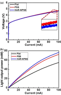
Fig. 4 shows the characteristics of a typical current–voltage
(I–V) and intensity–current (L–I) characteristics of conventional
LEDs with a flat sapphire substrate, LEDs with a PSS and LEDs
with a HAR-NPSS for transistor outline-can (TO-can) package.
It is found that the measured forward voltages under a injection
current of 20 mA at room temperature for conventional LEDs
with a flat sapphire substrate, LEDs with a PSS and LEDs with
a HAR-NPSS are 3.29, 3.3, 3.28 V, respectively. The voltages
of LEDs with a flat sapphire substrate, LEDs with a PSS and
LEDs with a HAR-NPSS are very close under a driving current
of 20 mA. It indicates the good electrical propertisy of LEDs
with a PSS and LEDs with a HAR-PSS. In addition, the I-V
curves of LEDs devices with a flat sapphire substrate, a PSS
and a HAR-NPSS are very similar even under a high injection
current. There is no influence to I–V characteristics of device
when we used a PSS or a HAR-PSS. At a an injection current
of 20 mA and peak wavelength of 460 nm for TO-can package,
the light output powers of conventional LEDs with a flat
sap-phire substrate, LEDs with a PSS and LEDs with a HAR-NPSS
are measured of 14.7, 20.3 and 22 mW by a integrating sphere
Fig. 4. (a) Current–voltage (I–V) characteristics of conventional LEDs with a flat sapphire substrate, a PSS and a HAR-NPSS. (b) Intensity–current (L–I) characteristics of conventional LEDs with a flat sapphire substrate, a PSS and a HAR-NPSS.
measurement system. Hence, the enhancement percentages of
LEDs with a PSS and LEDs with a HAR-NPSS are 38 and 49%
which are compared to conventional LEDs with a flat sapphire.
The optical enhancements are attributed to the improvement of
GaN crystal quality by PSS and HAR-NPSS, and the pattern
ge-ometry of PSS or HAR-PSS is not critical factor to reduce the
defects in the GaN layers. The calculated value of wall plug
effi-ciency (WPE) are 22.3, 30.7 and 33.5% for conventional LEDs
with a flat sapphire substrate, LEDs with a PSS and LEDs with
a HAR-NPSS. The enhancement of the WPE of LEDs with a
HAR-NPSS can be attributed to IQE and LEE of the device.
The IQE of LEDs grown on a HAR-NPSS and PSS are
sim-ilar due to they have almost the same dislocation densities. On
the other hand, the LED with a HAR-NPSS has a higher output
power than the LED with a NPSS, which is attributed to the light
scattering effect by nano-scale HAR-NPSS.
As compared to the previous work [29], the aspect ratios of
the structure with NPSS and embedded SiO nanorod array and
the structure with HAR-NPSS in this paper are indeed much
dif-ferent. The aspect ratio of the former structure is approximately
0.4, while it of the current structure is approximately 1.12.
How-ever, we should note that the 48% of light output power
en-hancement is contributed from both effects of the NPSS and
em-bedded SiO nanorod array. For the LED only with the NPSS
structure, the light output power enhancement is only 35% [29].
In addition, the chip sizes between these two researches are
dif-ferent. The LEDs with the NPSS and embedded SiO nanorod
array are 300
300 m , while the LEDs with the HAR-NPSS
are 575
250 m . In addition, the advantages of using the
HAR-NPSS as the epitaxial substrate is that it can further
im-prove the crystalline quality and LEE without the complicated
technique. The light output power enhancement of LEDs with
HAR-NPSS can achieve the same level (49%) as compared
with the previous work (48%). However, the layer thickness of
un-doped GaN should be increased, so the GaN epi-layer can
effectively coalesce. But we consider that the layer thickness
in-crease is acceptable because the thicker epi-layer is also needed
as using the commercial micro-scale PSS.
IV. C
ONCLUSIONIn short, GaN-based LEDs with a high aspect ratio
cone-shape nano-patterned sapphire substrate (HAR-NPSS)
are demonstrated with the nano-imprint lithography (NIL).
The light output power of the GaN-based LEDs grown on a
HAR-NPSS showed better performance as compared to LEDs
with a PSS and a unpatterned sapphire substrate. The high
output power of the LED with a HAR-NPSS indicated that
using NAR-NPSS as epitaxial substrate to grow LED structure
can not only improve the crystalline quality of GaN-based
LEDs but also enhance the light extraction efficiency. This
work verified that the HAR-NPSS has a promising potential to
improve performances of GaN-based LEDs. It also proved that
the NIL system is advantaged to fabricate a HAR-NPSS for
mass production.
A
CKNOWLEDGMENTThe authors thank Luxtaltek Corporation, Miaoli, Taiwan, for
their technical support.
R
EFERENCES[1] M. Koike, N. Shibata, H. Kato, and Y. Takahashi, “Development of high efficiency GaN based multi-quantum-well light-emitting diodes and their applications,” IEEE J. Sel. Topics Quantum Electron., vol. 8, pp. 271–277, 2002.
[2] E. F. Schubert, Light-Emitting Diodes. Cambridge, U.K.: Cambridge University Press, 2003.
[3] T. S. Oh, S. H. Kim, T. K. Kim, Y. S. Lee, H. Jeong, G. M. Yang, and E. K. Suh, “GaN-Based light-emitting diodes on micro-lens patterned sapphire substrate,” Jpn. J. Appl. Phys., vol. 47, no. 7, pp. 5333–5336, 2008.
[4] D. S. Wuu, W. K. Wang, K. S. Wen, S. C. Huang, S. H. Lin, R. H. Horng, Y. S. Yu, and M. H. Pan, “Fabrication of pyramidal patterned sapphire substrates for high-efficiency InGaN-Based light emitting diodes,” J. Electrochem. Soc., vol. 153, pp. G765–G770, 2006. [5] J. J. Chen, Y. K. Su, C. L. Lin, S. M. Chen, W. L. Li, C. C. Kao, J. J.
Chen, Y. K. Su, C. L. Lin, S. M. Chen, W. L. Li, and C. C. Kao, “En-hanced output power of GaN-Based LEDs with nano-patterned sap-phire substrates,” IEEE Photon. Technol. Lett., vol. 20, no. 13, pp. 1193–1195, 2008, Fellow, IEEE.
[6] Y.-K. Su, J.-J. Chen, C.-L. Lin, S.-M. Chen, W.-L. Li, and C.-C. Kao, “GaN-Based light-emitting diodes grown on photonic crystal-patterned sapphire substrates by nanosphere lithography,” Jpn. J. Appl. Phys., vol. 47, no. 8, pp. 6706–6708, 2008.
[7] H. Gao, F. Yan, Y. Zhang, J. Li, Y. Zeng, and G. Wang, “Enhancement of the light output power of InGaN/GaN light-emitting diodes grown on pyramidal patterned sapphire substrates in the micro- and nanoscale,” J. Appl. Phys., vol. 103, pp. 014314–014314-5, 2008.
[8] C.-C. Kao, Y.-K. Su, C.-L. Lin, and J.-J. Chen, “The aspect ratio effects on the performances of GaN-based light-emitting diodes with nanopatterned sapphire substrates,” Appl. Phys. Lett., vol. 97, pp. 023111-1–023111-3, 2010.
[9] Y.-K. Ee, J. M. Biser, W. Cao, H. M. Chan, R. P. Vinci, and N. Tansu, “Metalorganic vapor phase epitaxy of III-nitride light-emitting diodes on nanopatterned AGOG sapphire substrate by abbreviated growth mode,” IEEE J. Sel. Topics Quantum Electron., vol. 15, pp. 1066–1072, 2009, Student Member, IEEE.
Tansu, “Abbreviated MOVPE nucleation of III-nitride light-emitting diodes on nano-patterned sapphire,” J. Cryst. Growth, vol. 312, pp. 1311–1315, 2010.
[11] Y. Li, S. You, M. Zhu, L. Zhao, W. Hou, T. Detchprohm, Y. Taniguchi, N. Tamura, S. Tanaka, and C. Wetzel, “Defect-reduced green GaInN/GaN light-emitting diode on nanopatterned sapphire,” Appl. Phys. Lett., vol. 98, pp. 151102-1–151102-3, 2011.
[12] W. Cao, J. M. Biser, Y.-K. Ee, X.-H. Li, N. Tansu, H. M. Chan, and R. P. Vinci, “Dislocation structure of GaN films grown on planar and nano-patterned sapphire,” J. Appl. Phys., vol. 110, pp. 053505-1–053505-4, 2011.
[13] R. M. Farrell, E. C. Young, F. Wu, S. P. DenBaars, and J. S. Speck, “Materials and growth issues for high-performance nonpolar and semipolar light-emitting devices,” Semicond. Sci. Technol., vol. 27, pp. 024001-1–024001-14, 2012.
[14] D. A. Browne, E. C. Young, J. R. Lang, C. A. Hurni, and J. S. Speck, “Indium and impurity incorporation in InGaN films on polar, nonpolar, and semipolar GaN orientations grown by ammonia molecular beam epitaxy,” J. Vacuum Sci. Technol. A, vol. 30, pp. 041513-1–041513-8, 2012.
[15] P. S. Hsu, M. T. Hardy, F. Wu, I. Koslow, E. C. Young, A. E. Ro-manov, K. Fujito, D. F. Feezell, S. P. DenBaars, J. S. Speck, and S. Nakamura, “444.9 nm semipolar (1122) laser diode grown on an inten-tionally stress relaxed InGaN waveguiding layer,” Appl. Phys. Lett., vol. 100, pp. 021104-1–021104-4, 2012.
[16] H. Zhao, G. Liu, J. Zhang, J. D. Poplawsky, V. Dierolf, and N. Tansu, “Approaches for high internal quantum efficiency green InGaN light-emitting diodes with large overlap quantum wells,” Opt. Express, vol. 19, pp. A991–A1007, 2011.
[17] J. Zhang and N. Tansu, “Improvement in spontaneous emission rates for InGaN quantum wells on ternary InGaN substrate for light-emitting diodes,” J. Appl. Phys., vol. 110, pp. 113110-1–113110-5, 2011. [18] J. Zhang and N. Tansu, “Optical gain and laser characteristics of InGaN
quantum wells on ternary InGaN substrates,” IEEE Photon. J., vol. 5, pp. 2600111-1–2600111-11, 2013.
[19] E. Matioli, B. Fleury, E. Rangel, T. Melo, E. Hu, J. Speck, and C. Weis-buch, “High extraction efficiency GaN-based photonic-crystal light-emitting diodes: Comparison of extraction lengths between surface and embedded photonic crystals,” Appl. Phys. Express, vol. 3, pp. 032103-1–032103-3, 2010.
[20] J. Jewell, D. Simeonov, S.-C. Huang, Y.-L. Hu, S. Nakamura, J. Speck, and C. Weisbuch, “Double embedded photonic crystals for extraction of guided light in light-emitting diodes,” Appl. Phys. Lett., vol. 100, pp. 171105-1–171105-4, 2012.
[21] X.-H. Li, R. Song, Y.-K. Ee, P. Kumnorkaew, J. F. Gilchrist, and N. Tansu, “Light extraction efficiency and radiation patterns of III-Nitride light-emitting diodes with colloidal microlens arrays with various as-pect ratios,” IEEE Photon. J., vol. 3, pp. 489–499, 2011.
[22] Y.-K. Ee, P. Kumnorkaew, R. A. Arif, H. Tong, J. F. Gilchrist, and N. Tansu, “Light extraction efficiency enhancement of InGaN quantum wells light-emitting diodes with polydimethylsiloxane concave mi-crostructures,” Opt. Express, vol. 17, pp. 13747–13757, 2009. [23] H. Y. Lin, Y. J. Chen, C. C. Chang, X. F. Li, S. C. Hsu, and C. Y. Liu,
“Pattern-coverage effect on light extraction efficiency of GaN LED on patterned-sapphire substrate,” Electrochem. Solid-State Lett., vol. 15, pp. H72–H74, 2012.
[24] H.-W. Huang, J.-K. Huang, S.-Y. Kuo, K.-Y. Lee, and H.-C. Kuo, “High extraction efficiency GaN-based light-emitting diodes on embedded SiO2 nanorod array and nanoscale patterned sapphire substrate,” Appl. Phys. Lett., vol. 96, p. 263115, 2010.
[25] Z. S. Zhang, B. Zhang, J. Xu, K. Xu, Z. J. Yang, Z. X. Qin, T. J. Yu, and D. P. Yu, “Effects of symmetry of GaN-based two-dimensional photonic crystal with quasicrystal lattices on enhancement of surface light extraction,” Appl. Phys. Lett., vol. 88, pp. 171103-1–171103-3, 2006.
[26] C.-C. Chen, C.-H. Chiu, P.-M. Tu, M.-Y. Kuo, M. H. Shih, J.-K. Huang, H.-C. Kuo, H.-W. Zan, and C.-Y. Chang, “Large area of ultraviolet GaN-based photonic quasicrystal laser,” Jap. J. Appl. Phys., vol. 51, pp. 04DG02-1–04DG02-3, 2012.
[27] C.-C. Chen, C.-H. Chiu, S.-P. Chang, M. H. Shih, M.-Y. Kuo, J.-K. Huang, H.-C. Kuo, S.-P. Chen, L.-L. Lee, and M.-S. Jeng, “Large-area ultraviolet GaN-based photonic quasicrystal laser with high-efficiency green color emission of semipolar {10–11} mul-tiple quantum wells,” Appl. Phys. Lett., vol. 102, p. 011134, 2013.
[28] C. H. Chiu, H. H. Yen, C. L. Chao, Z. Y. Li, P. C. Yu, H. C. Kuo, T. C. Lu, S. C. Wang, K. M. Lau, and S. J. Cheng, “Nanoscale epi-taxial lateral overgrowth of GaN-based light-emitting diodes on a SiO nanorod-array patterned sapphire template,” Appl. Phys. Lett., vol. 93, pp. 081108-1–081108-3, 2008.
[29] H.-W. Huang, J.-K. Huang, S.-Y. Kuo, K.-Y. Lee, and H.-C. Kuo, “High extraction efficiency GaN-based light-emitting diodes on embedded SiO nanorod array and nanoscale patterned sapphire substrate,” Appl. Phys. Lett., vol. 96, pp. 263115-1–263115-3, 2010.
Jhih-Kai Huang received the B.S. degree in
Department of Electrical Engineering, from Na-tional Central University and the M.S. degree in electro-optical engineering from National Chiao Tung University, Hsinchu, Taiwan, in 2007 and 2009, respectively, and is currently working toward the Ph.D. degree in the Institute of Electro-Optical Engineering, National Chiao Tung University, Hsinchu, Taiwan.
His research areas include GaN-based device fab-rication and nano-imprint technology and nano-struc-ture process for GaN-based light-emitting diodes.
Da-Wei Lin received the B.S. and the M.S. degrees in
Department of Photonics from National Chiao Tung University, Hsinchu, Taiwan, in 2009 and 2010, re-spectively, and is currently working toward the Ph.D. degree in the Department of Photonics.
His research areas include the epitaxy of III-V compound semiconductor materials by MOCVD and analysis for GaN-based light-emitting diodes.
Min-Hsiung Shih (A’10–M’12) received B.S degree
in physics from the National Cheng Kung University, Tainan, Taiwan, in 1995, the M.S. degree in physics from the National Tsing Hua University (NTHU), Taiwan in 1997, and the Ph.D. degree in electrical engineering/electrophysics from the University of Southern California (USC), Los Angeles, USA, in 2006.
He is currently an Associate Research Fellow in the Research Center for Applied Sciences (RCAS), Academia Sinica, Taiwan, and an Adjunct Associate Professor in Department of Photonics, National National Chiao Tung Univer-sity (NCTU), Taiwan. His research interests include integrated photonic circuits, photonic crystals, GaN-based lasers, surface plasmonics, and cavity quantum electrodynamics. He had authored more than 80 journal and conference publi-cations.
Prof. Shih is a member of the Optical Society of America (OSA).
Kang-Yuan Lee received the B.S. degree in physics
from the National Sun Yat-sen University, Kaoh-siung, Taiwan, in 1996, and the M.S. and Ph.D degrees in electro-optical engineering from National Chiao Tung University, Hsinchu, Taiwan, in 1998 and 2005, respectively.
From 2000 to 2001, he was an Engineer with the Photo Lithography Division in TSMC. From 2006 to 2008, he was the R&D section Manager with Asia Optical Corporation. He is currently working in the Luxtaltek Corporation, Chunan, Taiwan. His research interests include optical measurement, GaN-based light-emitting devices and nano-structure fabrication.
Jyun-Rong Chen was born in Taichung, Taiwan,
on October 23, 1980. He received the B.S. degree in physics from the National Changhua University of Education (NCUE), Changhua, Taiwan, in 2004, and the M.S. degree in optoelectronics from the Institute of Photonics, NCUE, in 2006, and is currently working toward the Ph.D. degree at the Department of Photonics and the Institute of Electro-Optical En-gineering, National Chiao Tung University (NCTU), Hsinchu, Taiwan.
In 2006, he was with the Semiconductor Laser Technology Laboratory, NCTU, where he was engaged in research on III-V semiconductor materials for LEDs and semiconductor lasers. His current research interests include III-nitride semiconductor lasers, epitaxial growth of III-nitride materials, and numerical simulation of III-V optoelectronic devices.
Hung-Weng Huang, photograph and biography not available at time of
publication.
Shou-Yi Kuo was born in Taiwan, R.O.C. He
received the B.S. degree in Electrical and Control Engineering from National Chiao Tung University (NCTU), Hsinchu, Taiwan, R.O.C., in 1995, and the M.S. and Ph.D. degrees in Electro-Optical Engi-neering from NCTU, in 1997 and 2002, respectively. After he received his Ph.D. degree, he joined In-strument Technology Research Center, National Ap-plied Research Laboratories, Hsinchu Taiwan, as an associate researcher since January 2003. His main re-search interests and working experiences are focused on fabrication and characterizing of III-V and II-V wide-bandgap semiconduc-tors, including GaN, ZnO, InN and dilute nitrides. He has been authored and co-authored more than 35 international Journals and 2 patents related to III-V compound semiconductor devices technology
Chung-Hsiang Lin received the B.S. and M.S.
de-grees in physics from National Taiwan University, Taipei, Taiwan. He also received the M.S. degree in electrical and computer engineering and the Ph.D. de-gree in physics from Polytechnic Institute of New York University, New York, USA.
He is the President of New Business Unit of Luxtaltek Corporation, Miaoli, Taiwan, and serves as an adjunct professor at the Institute of Electro-Op-tical Engineering, National Chiao Tung University (NCTU), Taipei, Taiwan. He has over 10 years of experience in the LED industry, specifically photonic crystal modeling and nano-fabrication on optoelectronic devices. He has over 30 professional publications related to photonic crystal devices. Prior to joining Luxtaltek, he held several research positions including a visiting scholar with Jet Propulsion Laboratory, Pasadena, CA, USA.
Po-Tsung Lee (M’06) received the B.S. degree
from the Department of Physics, National Taiwan University (NTU), Taipei, Taiwan, in 1997 and the M.S. and Ph.D. degrees from the Department of Electrical Engineering-Electrophysics, University of Southern California (USC), Los Angeles, USA, in 1998 and 2003, respectively. During the Ph.D. study, she was engaged in photonic crystal microcavity lasers.
In 2003, she joined the Institute of Electro-Op-tical Engineering, National Chiao Tung University (NCTU), Hsinchu, Taiwan, as an Assistant Professor. In 2007, she became an Associate Professor in the Department of Photonics, NCTU. Her recent
and their applications, metallic nanostructures with localized surface plasmon resonances, and silicon-based solar cell technologies.
Prof. Lee was the recipient of the University of Southern California Women in Science and Engineering (WISE) Award in 2000–2001. She received the “Out-standing Young Electrical Engineer Award” from the Chinese Institute of Elec-trical Engineering in 2011.
Gou-Chung Chi was born on September 8, 1946, in
Kaohsiung, Taiwan, R.O.C. He received the B.S. de-gree from the National Taiwan Normal University, Taiwan, in 1970, and the M.S. and Ph.D. degrees in solid state physics and materials, Department of En-gineering and Applied Science from Yale University, new Haven CT, USA, in 1973 and 1976, respectively. From 1977 to 1990, he was a Member of the Tech-nical Staff at AT&T Bell Laboratories. From 1990 to 1994, he was a director of the division of optoelec-tronics materials and devices at Opto-Elecoptoelec-tronics & Systems Laboratories (OES) of Industrial Technology Research Institute (ITRI), Taiwan. From 1994, he had been a professor and director of Optical Sciences Center, National Central University. Since 2009, he is a professor of Depart-ment of Photonics, National Chiao Tung University, Hsinchu, Taiwan. His re-cent research interests are wide band gap semiconductor and devices (A1GaInP, InGaAsP, GaN-based materials), and microoptics integrated system.
Dr. Chi is also a member of Materials Research Society, Physical Society (Taiwan), Electrocins Devices and Materials Association (Taiwan).
B.S. degree in physics from the National Taiwan University, Taipei, Taiwan, in 1990, the M.S. degree in electrical and computer engineering from Rutgers University, Camden, NJ, in 1995, and the Ph.D. degree in electrical and computer engineering from the University of Illinois at Urbana-Champaign, Urbana, Illinois, in 1999.
He has an extensive professional career both in re-search and industrial rere-search institutions. From 1995 to 1997, he was a Research Consultant with Lucent Technologies, Bell Lab, Holmdel, NJ. From 1999 to 2001, he was an R&D Engi-neer with the Fiber-Optics Division, Agilent Technologies. From 2001 to 2002, he was the R&D Manager with LuxNet Corporation. Since September 2002, he has been a member of the faculty at the Institute of Electro-Optical Engineering, National Chiao Tung University (NCTU), Hsinchu, Taiwan. He has authored or coauthored over 60 publications. His current research interests include the epi-taxy, design, fabrication, and measurement of high-speed InPand GaAs-based vertical-cavity surface-emitting lasers, as well as GaN-based lighting-emitting devices and nanostructures.