This content has been downloaded from IOPscience. Please scroll down to see the full text.
Download details:
IP Address: 140.113.38.11
This content was downloaded on 25/04/2014 at 00:58
Please note that terms and conditions apply.
Investigation of low-temperature electroluminescence of InGaN/GaN based nanorod light
emitting arrays
View the table of contents for this issue, or go to the journal homepage for more 2011 Nanotechnology 22 045202
(http://iopscience.iop.org/0957-4484/22/4/045202)
Nanotechnology 22 (2011) 045202 (6pp) doi:10.1088/0957-4484/22/4/045202
Investigation of low-temperature
electroluminescence of InGaN/GaN based
nanorod light emitting arrays
Ying-Yuan Huang
1, Liang-Yi Chen
1, Chun-Hsiang Chang
1,
Yu-Hsuan Sun
1, Yun-Wei Cheng
1, Min-Yung Ke
1,
Yu-Hsin Lu
2, Hao-Chung Kuo
2and JianJang Huang
1,31Graduate Institute of Photonics and Optoelectronics, National Taiwan University, 1,
Roosevelt Road, Section 4, Taipei 106, Taiwan
2Department of Photonics, National Chiao Tung University, Hsinchu 300, Taiwan 3Department of Electrical Engineering, National Taiwan University, 1, Roosevelt Road,
Section 4, Taipei 106, Taiwan E-mail:[email protected]
Received 29 July 2010, in final form 8 October 2010 Published 15 December 2010
Online atstacks.iop.org/Nano/22/045202
Abstract
For InGaN/GaN based nanorod devices using a top-down etching process, the optical output power is affected by non-radiative recombination due to sidewall defects (which decrease light output efficiency) and the mitigated quantum confined Stark effect (QCSE) due to strain relaxation (which increases internal quantum efficiency). Therefore, the exploration of low-temperature optical behaviors of nanorod light emitting diodes (LEDs) will help identify the correlation between these two factors. In this work, low-temperature electroluminescent (EL) spectra of InGaN/GaN nanorod arrays were explored and compared with those of planar LEDs. The nanorod LED exhibits a much higher optical output percentage increase when the temperature decreases. The increase is mainly attributed to the increased carriers in the
quantum wells for radiative recombination. Also, due to a better spatial overlap of electrons and holes in the quantum wells, the increased number of carriers can be more efficiently recombined in the nanorod device. Next, while the nanorod array shows nearly constant peak energy in the EL spectra at various injection currents at the temperature of 300 K, a blue shift has been observed at 190 K. The results suggest that with less non-radiative recombination and thus more carriers in the quantum wells, carrier screening and band filling still prevail in the partially strain relaxed nanorods. Moreover, when the temperature drops to 77 K, the blue shift of both nanorod and planar devices disappears and the optical output power decreases since there are fewer carriers in the quantum wells for radiative recombination.
(Some figures in this article are in colour only in the electronic version)
1. Introduction
III-nitride wide bandgap semiconductors have been widely used in optoelectronic devices, such as blue and green light emitting diodes. While most commercial LEDs are fabricated based on the planar structure, nanostructure light sources have attracted considerable attention as they may have the potential of better light extraction due to the increased sidewall areas and higher radiation directionality due to the vertical light
guiding effect along the rods [1, 2]. In the past couple of years, GaN based nanorod LED arrays have been fabricated and characterized at room temperature [1–6]. Strain relaxation in the InGaN/GaN multiple quantum well (MQW) layers has resulted in a reduced quantum confined Stark effect (QCSE) [3,7] and thus the peak wavelength is nearly constant with various injection currents [3]. On the other hand, the top-down etching induced sidewall damage has created a large amount of defects and leakage currents that limit the
Nanotechnology 22 (2011) 045202 Y-Y Huang et al light output power. We previously demonstrated nanorod
LED arrays with low reverse bias leakage using the chemical mechanical polishing (CMP) process [8]. For such a nanorod device, the optical output power is balanced between the effects of non-radiative recombination due to sidewall defects (which decrease light output efficiency) and the mitigated QCSE due to strain relaxation (which increases internal quantum efficiency). Therefore, the exploration of low-temperature optical behaviors of nanorod LEDs will help identify the correlation between these two factors.
In this work, we first performed Raman scattering measurements to identify strain relaxation in the InGaN/GaN quantum well region of both the nanorod and planar structures. In the next step, optical output power and electroluminescent (EL) spectra at temperatures between 300 and 77 K of the nanorod devices were extracted and compared with those of the planar devices.
2. Fabrication of nanorod LED arrays
The LED epitaxial growth and nanorod array fabrication are similar to those described in our previous work [8]. In short, the GaN based LED sample is grown by metal organic chemical vapor deposition (MOCVD) on a c-plane sapphire substrate. The material structure is composed of a 2 µm Si doped n-type GaN layer, a five-period of In0.2Ga0.8N/GaN
multiple quantum well (MQW) structure, and a 160 nm Mg doped p-type GaN layer. The nanorod array was achieved by performing nanosphere lithography in the LED epi-structure [3]. The nanorod diameter is around 100± 10 nm and the rod etching depth is about 500 nm (see figure1(a) for the scanning electron microscopic (SEM) cross-section image of the nanorod array). The sample can then be employed for Raman scattering measurements to reveal the strain properties of the nanostructure. The nanorod array was defined in a mesa pattern with a size 250× 250 µm2. In order to prevent
electric shorting between contacts on the p-type and n-type layers, we filled the nanorod spacing with a 300 nm thick SOG (spin-on glass) layer using a reflow process at 130◦C for 10 min. The SOG can also serve to passivate sidewall defects induced during the ICP etching. Next, a CMP process employing Al2O3particle slurry with diameter around 800 nm
was applied to remove the SiO2deposited right on the tips of
the nanorods. Details of the CMP process are described in our previous research [8]. In the last step, via holes were opened by RIE (reactive ion-etching) to enable the deposition of the n-type (Au/Ti (120 nm/10 nm)) contact electrodes. Finally a thin metal stack (Au/Ni 5 nm/5 nm) was coated for current spreading (p-thin layer) and the p-type contact electrode (Au/Ti 120 nm/10 nm) was then deposited. The schematic diagram of the nanorod LED array is shown in figure1(b).
3. Results and discussion
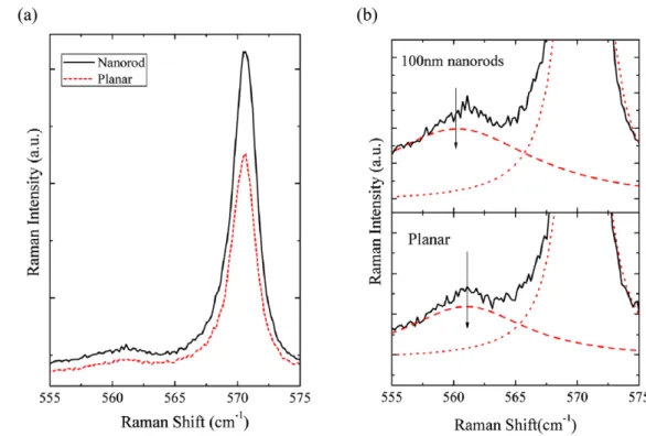
Figure 2 shows Raman spectra of the nanorod epi-structure. For comparisons, the results of the planar LED structure are also shown. Basically, two phonon modes are identified from the Raman spectra. The peak near 569 cm−1corresponds to the
Figure 1. (a) Cross-section SEM image of the nanorod arrays.
(b) Schematic diagram of the nanorod LED arrays.
EH
2 mode of GaN (see figure2(a)) [9,10], while the shoulder
line around 560 cm−1is the EH
2 mode of InGaN (see the
close-up view in figure2(b)) [11]. The InGaN EH
2 phonon mode of
nanorods shows a lower wavenumber than that of the planar structure. Since the 100 nm diameter nanorods are not small enough for the effect of phonon confinement, the Raman shift toward a lower frequency in the nanorod structure is mainly due to strain relaxation [11,12].
We next performed EL measurement on the nanorod devices at low temperature. The optical output at injection currents from 2 to 20 mA is demonstrated in figure3(a). To illustrate the percentage increase, the curves are normalized to the EL intensity at the temperature of 300 K and plotted in figure 3(b). From 300 to 190 K, the EL intensity of the nanorod LED array increases as the temperature is decreased. At 20 mA, the EL intensity increases by 55.4% when the temperature drops from 300 to 190 K. It is also observed that within the range of the injection current (2– 20 mA), the normalized EL intensity shows similar behaviors. The optical intensity increase at low temperature has been widely discussed on planar LEDs by photoluminescent (PL) measurement [13,14], and is mainly attributed to the frozen defect states and the corresponding decrease of the non-radiative recombination. For comparisons, low-temperature EL results for a planar LED with the same mesa area 250 × 250 µm2were extracted and are shown in figure4(a) along with the normalized EL intensity in figure 4(b). The 2
Figure 2. (a) Room temperature Raman scattering spectra of the planar and 100 nm nanorod structures and (b) close-up view of the EH 2 mode
of InGaN.
variation of EL intensity between 300 and 190 K is relatively mild for the planar device. At the injection current 20 mA, the EL intensity reaches its maximum at 220 K and is 4.9% higher than that at 300 K. Since the effect of non-radiative recombination is more severe for nanorods due to sidewall etching, the higher percentage increase of EL intensity of nanorods at low temperature is mainly attributed to the frozen defect states. Furthermore, due to the relaxed strain in the nanorods, as compared with the planar epi-structure, the mitigated QCSE results in a better electron–hole overlap in the quantum wells. Thus the increased carriers (due to less recombination with the sidewall defects) in the quantum wells of nanorods have a better chance to be radiatively recombined than those of the planar devices.
When the temperature is lower than 190 K, both nanorod and planar devices show a remarkable reduction of EL intensity. The monotonic decrease of EL intensity with temperature can be explained by the phenomena of carrier overflow [15–17] and low effective hole concentration [18]. At low temperature, carriers that are designated to be captured by the MQW overflow to the cladding layer. They are then either extinguished due to non-radiative recombination or to radiative recombination in the GaN cladding layer. Light emission at 3.3 eV at the temperature 77 K (see figure5) supports the above statement. This explanation is also consistent with previous research that carriers escape from the MQW region at low temperature [15,16]. Also, at low temperature, the activation energy of Mg dopants is increased and thus the effective hole concentration becomes lower [19], leading to less efficient radiative recombination. As a result, when the temperature drops below 190 K, the effect of EL intensity decreases since carrier overflow and low-effective hole concentration
become more significant than the enhancement of radiative recombination. Also, for the nanorods, at the temperature onset of 190 K, a sharp decrease of EL intensity is observed. Since the EL emission intensity depends on the balance of the frozen defect states, carrier overflow and effective carrier concentration, the sharp EL intensity decrease of nanorods at temperatures between 190 and 160 K indicates a dominant role of carrier overflow in the nanostructure.
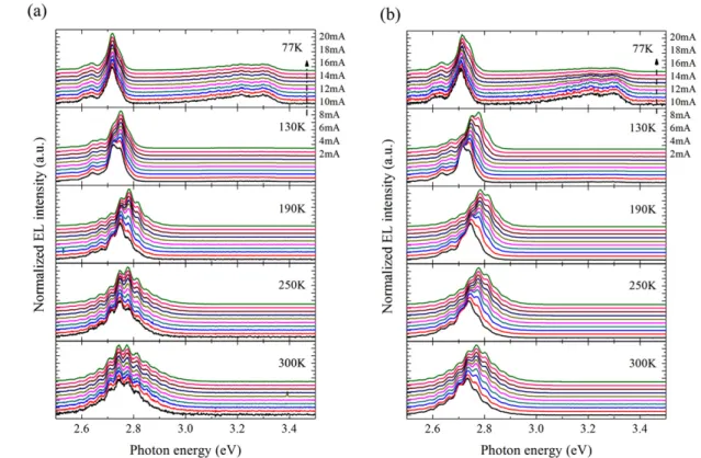
The effect of QCSE on EL light output at low temperature leads us to further explore the EL spectra at low temperature. The EL spectra of a nanorod array and a planar LED at an injection current from 2 mA to 20 mA are shown in figures 5(a) and (b), respectively. They reveal several interesting phenomena. First, at 300 K, the EL spectra of the nanorod LED possess nearly constant photon energy of around 2.76 eV, while those of the planar LED are blue shifted from 2.73 to 2.77 eV. The blue shift of planar LEDs is attributed to the carrier screening due to QCSE [3] and band filling of localized states [20].
The behavior of the EL spectra of a nanorod LED array at low temperature becomes different from that at room temperature. As the temperature declines to 190 K, the EL spectra start to show a blue shift from 2.75 to 2.78 eV with the increase of current from 2 to 20 mA for the nanorod LED array, while the blue shift for the planar LED becomes even stronger. From the EL intensity in figure3, a large portion of the injected carriers that should have been non-radiatively recombined with defects at room temperature now appear in the quantum wells in the nanorod structure. Thus, despite the mitigated QCSE for nanorod LEDs, the effect of band filling still prevails and blue shift can be observed as more injected carriers contribute to radiative light emission [20]. Also, from figure 5, at the
Nanotechnology 22 (2011) 045202 Y-Y Huang et al
Figure 3. EL intensity at various temperatures (a) and normalized EL intensity (assuming 1.0 at 300 K) (b) of the nanorod LED array.
Figure 4. EL intensity at various temperatures (a) and normalized EL intensity (assuming 1.0 at 300 K) (b) of the planar LED.
injection current of 20 mA, the emission energy shifts from 2.76 eV at 300 K to 2.78 eV at 190 K for nanorod LEDs, as compared with a shift from 2.77 eV at 300 K to 2.78 eV at 190 K for planar devices. The blue shift of the emission energy at lower temperature is mainly due to the Varshni law [21]. However, the effect of band filling at low temperature results in more blue shift for nanorod devices. Furthermore, the blue shift of the EL peak photon energy with the current increase becomes weaker as we cool the temperature from 190 to 77 K, which is correlated to the less pronounced effect of band filling. It is intriguing to observe that at 77 K, the blue shift of the EL spectra vanishes in both nanorod and planar LEDs. The absence of the blue shift indicates that carriers are not effectively captured by the MQW, implying carrier overflow at low temperature. As shown in both figures5(a) and (b), at 77 K, light emission at around 3.3 eV, which corresponds to the band edge transition in the GaN layers, is observed. At such a temperature, the effect of band filling related blue shift becomes less significant.
4. Conclusion
Low-temperature EL properties of InGaN/GaN nanorod arrays have been explored and compared with planar LEDs. It
is found that the optical output of a nanorod LED array increases by 55.4% when the temperature drops from 300 to 190 K, while there is only a 4.9% increase to the maximum output power at 220 K for a planar LED. We believe that the increase can be mainly attributed to the suppressed non-radiative recombination. Also, due to a better spatial overlap of electrons and holes in the quantum wells, carriers can be more efficiently recombined in the nanorod device at low temperature. Furthermore, as the temperature drops below 190 K, the optical intensity shows a monotonical decrease for both the planar and nanorod devices, which is mainly associated with carrier overflow to the GaN cladding layers and to the frozen Mg+dopant in the p-GaN layer. Next, while the nanorods show nearly constant peak energy in the EL spectra at various injection currents at 300 K, a blue shift from 2.75 to 2.78 eV has been observed at 190 K. The results suggest that with the increased number of carriers in the quantum wells (less non-radiative recombination), carrier screening and band filling still prevail in the partial strain relaxed nanorods. Moreover, when the temperature drops to 77 K, the blue shift of both nanorod and planar devices disappears as there are fewer carriers in the quantum wells for radiative recombination. 4
Figure 5. Normalized EL spectra of (a) nanorod and (b) planar LEDs at 77, 130, 190, 250, and 300 K. The injection current ranges from 2 to
20 mA.
Acknowledgment
This work was supported by the National Science Council of Taiwan under the grants NSC 97-2221-E-002-054-MY3.
References
[1] Ke M-Y, Wang C-Y, Chen L-Y, Chen H-H, Chiang H-L, Cheng Y-W, Hsieh M-Y, Chen C-P and Huang J 2009 Application of nanosphere lithography to LED surface texturing and to the fabrication of nanorod LED arrays
IEEE J. Sel. Top. Quantum Electron.15 1242–9
[2] Chiu C, Lu T, Huang H, Lai C, Kao C, Chu J, Yu C, Kuo H, Wang S and Lin C 2007 Fabrication of InGaN/GaN nanorod light-emitting diodes with self-assembled Ni metal islands
Nanotechnology18 445201
[3] Wang C-Y, Chen L-Y, Chen C-P, Cheng Y-W, Ke M-Y, Hsieh M-Y, Wu H-M, Peng L-H and Huang J 2008 GaN nanorod light emitting diode arrays with a nearly constant electroluminescent peak wavelength Opt. Express
16 10549–56
[4] Lee Y-J, Lin S-Y, Chiu C-H, Lu T-C, Kuo H-C, Wang S-C, Chhajed S, Kim J K and Schubert E F 2009 High output power density from GaN-based two-dimensional nanorod light-emitting diode arrays Appl. Phys. Lett.94 141111
[5] Wu Y-R, Chiu C, Chang C-Y, Yu P and Kuo H-C 2009 Size-dependent strain relaxation and optical characteristics of InGaN/GaN nanorod LEDs IEEE J. Sel. Top. Quantum
Electron.15 1226–33
[6] Kim H-M, Cho Y-H, Lee H, Kim S I, Ryu S R, Kim D Y, Kang T W and Chung K S 2004 High-brightness light emitting diodes using dislocation-free indium gallium nitride/gallium nitride multiquantum-well nanorod arrays
Nano Lett.4 1059–62
[7] Chen H, Yeh D, Lu Y, Chen C, Huang C, Tang T, Yang C and Wu C 2006 Strain relaxation and quantum confinement in InGaN/GaN nanoposts Nanotechnology17 1454
[8] Chen L-Y, Huang Y-Y, Chang C-H, Sun Y-H, Cheng Y-W, Ke M-Y, Chen C-P and Huang J 2010 High performance InGaN/GaN nanorod light emitting diode arrays fabricated by nanosphere lithography and chemical mechanical polishing processes Opt. Express18 7664–9
[9] Chen C H, Chen W H, Chen Y F and Lin T Y 2003 Piezoelectric, electro-optical, and photoelastic effects in InxGa1−xN/GaN multiple quantum wells Appl. Phys. Lett.
83 1770–2
[10] Kontos A, Raptis Y, Pelekanos N, Georgakilas A, Bellet-Amalric E and Jalabert D 2005 Micro-Raman characterization of InxGa1−xN/GaN/Al2O3heterostructures
Phys. Rev. B72 155336
[11] Liang C H, Chen L C, Hwang J S, Chen K H, Hung Y T and Chen Y F 2002 Selective-area growth of indium nitride nanowires on gold-patterned Si(100) substrates Appl. Phys.
Lett.81 22–4
[12] Chang H, Hsieh Y, Chen T, Chen Y, Liang C, Lin T, Tseng S and Chen L 2003 Strong luminescence from strain relaxed InGaN/GaN nanotips for highly efficient light emitters Appl. Phys. Lett.82 880–2
[13] Feng S, Cheng Y, Chung Y, Yang C, Lin Y, Hsu C, Ma K and Chyi J 2002 Impact of localized states on the recombination dynamics in InGaN/GaN quantum well structures J. Appl.
Phys.92 4441
[14] Leroux M, Grandjean N, Beaumont B, Nataf G, Semond F, Massies J and Gibart P 1999 Temperature quenching of photoluminescence intensities in undoped and doped GaN
J. Appl. Phys.86 3721–8
[15] Cao X, LeBoeuf S, Rowland L, Yan C and Liu H 2003 Temperature-dependent emission intensity and energy shift in InGaN/GaN multiple-quantum-well light-emitting diodes
Nanotechnology 22 (2011) 045202 Y-Y Huang et al
[16] Hori A, Yasunaga D, Satake A and Fujiwara K 2001
Temperature dependence of electroluminescence intensity of green and blue InGaN single-quantum-well light-emitting diodes Appl. Phys. Lett.79 3723
[17] Hori A, Yasunaga D, Satake A and Fujiwara K 2003 Temperature and injection current dependence of electroluminescence intensity in green and blue InGaN single-quantum-well light-emitting diodes J. Appl. Phys.
93 3152–7
[18] Kim D J, Ryu D Y, Bojarczuk N A, Karasinski J, Guha S, Lee S H and Lee J H 2000 Thermal activation energies of
Mg in GaN:Mg measured by the Hall effect and admittance spectroscopy J. Appl. Phys.88 2564–9
[19] Wang C, Chen J, Chiu C, Kuo H, Li Y, Lu T and Wang S 2010 Temperature-dependent electroluminescence efficiency in blue InGaN-GaN light-emitting diodes with different well widths IEEE Photon. Technol. Lett.22 236–8
[20] Mukai T, Takekawa K and Nakamura S 1998 InGaN-based blue light-emitting diodes grown on epitaxially laterally overgrown GaN substrates Japan. J. Appl. Phys. 237 839–41
[21] Varshni Y 1967 Temperature dependence of the energy gap in semiconductors Physica34 149–54