國 立 交 通 大 學
電信工程研究所
碩 士 論 文
梯度人造磁導體的反射特性
Reflection Characteristics of a Gradient
Artificial Magnetic Conductor
研究生:許勝傑 (Sheng-Chieh Hsu)
指導教授:黃瑞彬 博士 (Dr.
Ruey-Bing Hwang
)
梯度人造磁導體的反射特性
Reflection Characteristics of a Gradient Artificial Magnetic
Conductor
研 究 生:許勝傑 Student:Sheng-Chieh Hsu
指導教授:黃瑞彬 博士 Advisor:Ruey-Bing Hwang
國 立 交 通 大 學 電信工程研究所 碩 士 論 文 A ThesisSubmitted to Institute of Communication Engineering College of Electrical Engineering
National Chiao Tung University In Partial Fulfillment of the Requirements
For the Degree of Master of Science
In
Communication Engineering August 2010
梯度人造磁導體的反射特性
學生:許勝傑 指導教授:黃瑞彬 博士 國立交通大學電信工程研究所碩士班摘要
我們研究了下方有著接地金屬的介質平版所組成二維正方形貼片陣列的電 磁反射特性。藉著改變金屬貼片的大小,兩兩相鄰的貼片會有一個相等的反射相 位差角。利用這個在陣列單元中等差遞增的反射相位特性,當一個垂直入射的平 面波打到這個結構時,他的反射波會被散射到我們所設計的方向。在這篇論文中, 我們根據陣列天線理論建立了一個簡單的公式來計算反射波的遠場場形。再者我 們使用一個時域全波模擬套裝軟體(CST)來精準地計算在結構中的電磁場分布以 及遠場場形。此外我們將這個結構實作出來並且在電磁無反射實驗室中量測他的 散射場型。經由這個實驗,我們量測到了很好的數據結果來驗證我們所提出的設 計原理和步驟。這樣的一個結構可以被用來應用在波束控制(beam steering)以及 減少雷達橫截面(radar cross section reduction)。Student: Sheng-Chieh Hsu Advisor: Dr. Ruey-Bing Hwang
Department of Communication Engineering National Chiao Tung University
Abstract
We studied the electromagnetic reflection of a two-dimensional square patches array backed with a grounded dielectric slab. By tuning the size of the metal patch, the adjacent two patches may have an equal reflected-phase angle. Using this property of progressively reflected-phase angle in the array elements, for a normal incident wave we can steer the reflected wave into a desired direction. In this thesis, we have established a simple formula based on the array antenna theory to figure out the reflected wave pattern. Moreover, a time-domain full-wave simulation package (CST) was employed to rigorously calculate the electromagnetic fields in the structure as well as the far-field pattern. Besides, we have fabricated the structure and measured its scattering pattern in an electromagnetic anechoic chamber. The excellent measured results confirm the design principle and procedures in this research. Such a planar structure may have potential applications in beam-tilting and radar cross section reduction.
Acknowledgement
首先要感謝我的指導老師黃瑞彬博士在我這兩年碩士生涯中的指導。舉凡從 理論基礎到實作量測和論文撰寫,老師都循序漸進地教導,我也才能這麼順利地 完成這份研究。此外本實驗室中的正元和岳霖學長,他們也提供我許多的想法和 解決問題的方法,使我受益良多。我的同儕宏麒、子淵和政皓,以及遠場量測實 驗室的漢維和健候,在研究之餘常常一起吃飯和打球,和他們一起討論使我更能 發現自己問題之所在,而讓我慢慢進步。我要特別感謝學弟肅哲,在最後量測階 段時,成為我最強力的助手。也要感謝其他學弟晟瑞、派宣、柏廷和宜哲,有了 他們使得我的碩士生活變得更多采多姿。 最後要感謝我的家人,爸爸、媽媽還有姊姊,有你們的支持我才能順利地完 成學業。還有一直陪伴身旁的女友盈穎,有著她的鼓勵我才有繼續向前的動力, 為我學生生涯畫下完美的句點。謝謝你們大家。Catalog
Chinese Abstract ... .i Abstract ... .ii Acknowledgement ... iii Catalog ... iv Figure Catalog ... v Table Catalog ... vi Chapter 1 Introduction ... 1Chapter 2 Structure Confuguration ... 4
Reflection phase of a 2D periodic structure consisting of metal patches array ... 4
Chapter 3 Numerical Analysis ... 8
3.1 Reflection characteristics of a gradient AMC surface ... 8
3.2 Array antenna factor ... 12
Chapter 4 Experimental Studies... 15
4.1 Bistatic RCS measurement ... 16
4.2 Monostatic RCS measurement ... 17
Chapter 5 Numerical Results, Experimental Results and Discussion... 19
5.1 Numerical Results ... 19
Patch size ... 19
Thickness of substrate ... 19
Dielectric constant ... 20
Unit cell dimension ... 21
Chapter 6 Applications ... 33
References ... 34
Figure Catalog
Figure 2-1 A gradient AMC surface consisting of square patches array ... 4Figure 2-2 (a) Schemetic Diagram for Normal Incident ... 6
(b) Period and Patch ... 6
(c) Wave Port with Reference Plane ... 6
(d) Boundary ... 6
Figure 2-3 Reflection phase for different patch dimensions ... 7
Figure 3-1 Reflection phase for patch dimensions a1 to a5 ... 9
Figure 3-2 CST environment setting ... 9
Figure 3-3 Far field scattering pattern over the x-z plane with (a) 1 period ... 10
(b) 2 periods ... 10
(c) 3 periods ... 10
(d) 6 periods ... 10
Figure 3-4 Electric field phase distribution along x-axis on the AMC surface ... 12
Figure 3-5 Comparison between array factor calculation result and CST simulation result ... 13
Figure 3-6 Relation between phase differences and reflection angle ... 14
Figure 4-1 Reflection phase angles distribution along periodic AMC surface ... 15
Figure 4-2 Measurement set-up ... 16
Figure 4-3 Bistatic RCS Measurement Schemetic Diagram ... 16
Figure 4-4 Bistatic RCS Measurement Pictures ... 16
Figure 4-5 Monostatic RCS Measurement Schemetic Diagram ... 17
Figure 5-1 Reflection Phase for Different Thickness of Substrate ... 20
Figure 5-2 Reflection Phase Angle versus Dielectric Constant ... 21
Figure 5-3 Reflection Phase Angle versus Period Size ... 22
Figure 5-4 Electric field distribution at (a) 36 cm from the horn ... 23
(b) 20 cm from the horn ... 23
Figure 5-5 Supercell AMC surface ... 24
Figure 5-6 3D pattern of supercell AMC surface for CST simulation ... 25
Figure 5-7 Bistatic RCS Measurement for supercell AMC surface at (a) 14.0 GHz ... 26 (b) 14.5 GHz ... 26 (c) 15.0 GHz ... 27 (d) 15.5 GHz ... 27 (e) 15.8 GHz ... 28 (f) 16.0 GHz ... 28
Figure 5-8 Monostatic RCS Measurement for supercell AMC surface at (a) 14.0 GHz ... 29 (b) 14.5 GHz ... 29 (c) 15.0 GHz ... 30 (d) 15.5 GHz ... 30 (e) 15.8 GHz ... 31 (f) 16.0 GHz ... 31
Figure 6-1 (a) B-2 Stealth bomber ... 33
Table 3 Resonance frequency against patch dimension ... 19 Table 4 Resonance frequency against thickness ... 20 Table 5 Resonance frequency against dielectric constant ... 21
Chapter 1 Introduction
Stealth technology has been intensively studied for military applications for many years. One figure out that with some special reflection coatings printed on an object the reflected electromagnetic wave can be further reduced; therefore, the radar system can’t allocate the object. With this motivation, we aimed at designing the artificial surface for Radar Cross Section (RCS) reduction.
The reflection phase of an incident plane wave on a perfect electric conductor (PEC) is 180 degree, but is zero degree for a perfect magnetic conductor (PMC). As revealed in [1], the Radar Cross Section (RCS) can be reduced by the chessboard-like structure consisting of PEC and Artificial Magnetic Conductor (AMC). Around the operational frequency of the AMC elements, the reflections of the AMC and PEC have opposite phase, so for the normal incident plane wave the reflections cancel out, thus reducing the RCS.
Regarding the AMC surface, a mushroom-type structure was designed and experimentally verified by Sievenpiper [2]. Such a structure is constructed using commonly used Printed Circuit Board (PCB) technology. It consists of rectangular patches array connecting to the ground plane through via holes. Notably, the dimensions of the rectangular patch are smaller than that of the operational wavelength. The unit cell of the structure resembles a cavity resonator. Around the resonance frequency, the input impedance looking into the cavity is larger than that of the free space intrinsic impedance, so it is named as a High Impedance Surface (HIS). With this high impedance characteristic, the reflected wave is in-phase with the incident wave, exhibiting the reflection characteristic of a perfect magnetic conductor.
capacitance between the patches and the resonance frequency of each unit cell. In addition to electrically tuning mechanism, the mechanically tuning method was also demonstrated in [5]. The mechanically tunable impedance surface consists of a high impedance ground and a separate tuning layer. The tuning layer is moved across the stationary high-impedance surface to vary the capacitance between the overlapping plates and tune the resonance frequency of the structure.
Artificial magnetic conductors for various metal shapes printed on the top of the surface have been studied [6]-[8]. As revealed in [6], a novel wideband artificial magnetic conductor (AMC) structure can act as high impedance surface covering the entire Ku-band from 12GHz to 18GHz for both TE and TM polarizations with respect to the angle of incidence. In [7], four kinds of Artificial Magnetic Conductors with rectangular lattices such as mushroom type high impedance surface, UC-PBG HIS, square patch and square loop Frequency selective surface (FSS) are analyzed and compared. The simulation results show that the loop FSS with smaller period has least sensitivity to the incident angle. A novel planar artificial magnetic conductor based on a frequency-selective surface has demonstrated for the application of frequencies below 1GHz, as shown in [8]. Besides, a simultaneous multi beam reflect-array has designed and validated by the experiment result. The measurements for near-field and far-field method are also discussed in [10].
The organization of this thesis is given as follows. In the next section, the structure configuration and the incident condition will be described. Secondly, the unit cell approach for determining the reflected phase angle of the AMC surface will be introduced. Moreover, the full structure simulation using CST Microwave Studio will be employed to calculate the scattering pattern of the AMC surface incident by a plane wave. In addition to the full-wave simulation, the simple formula based on the array antenna theory was developed for serving as an engineering design criterion. In the
successive section, we have fabricated the AMC surfaces and measured their reflection characteristics including the mono-static and bi-static RCS.
Chapter 2 Structure Configuration
Reflection phase of a 2D periodic structure consisting of metal
patches array
As mentioned previously, a PEC surface can reflects a 180-degree phase shift with respect to the incident plane wave, while a PMC surface can have an in-phase reflected wave. As was well known, so far, the nature PMC were not found. Nevertheless, the artificial PMC (named as artificial magnetic conductor throughout this thesis) can be realized by printing periodic metallic patterns on a grounded substrate, as will become clear later on. In this section, the structure with the reflection characteristics of AMC in a certain bandwidth will be first introduced. Moreover, the parametric studies on the reflected phase angle against the dimension of the metal patch will be carried out to provide us a design criterion for designing a beam-steerable reflection surface. Secondly, the AMC with the square-patch dimensions arranged in specific.
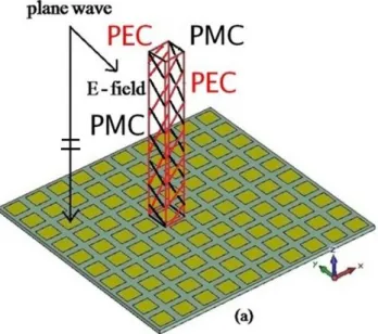
A two-dimensional periodic structure consisting of square metal patches printed on a substrate backed with metal ground plane is depicted in Fig. 2-1. Here, the structure is assumed to be infinite in extent along the x and y directions. The periods (unit-cell size) along the x- and y- axis are the same (denoted as d) and much smaller than that of the operational wavelength. The dimension of the square metal patch in each unit cell is denoted as a. A uniform plane wave is normally incident on the structure with its electric field along the y-axis. Notably, since the period d is assumed to be much smaller than that of the operation wavelength, all the higher space harmonics excluding (0, 0) will become evanescent (non-propagation) waves. The reflection characteristics of the infinite structure can be obtained through the unit cell approach. Due to the normal incidence and electric-field vector along the y-axis, the unit cell is a rectangular tube with the two PEC walls along the y-axis and two PMC walls along the x-axis, respectively, as demonstrated in Fig.2-2(a). Such a unit cell structure can be regarded as a waveguide filled with inhomogeneous medium and terminated by a metal plate at its bottom surface, such as in Fig. 2-2(b) (c) (d). Furthermore, due to the boundary conditions given in the unit cell, the fundamental waveguide mode is TEM wave with its electric and magnetic fields along the y and x axes, respectively.
By resolving the scattering analysis of the waveguide mode by the discontinuity containing inhomogeneous medium and metal patch, the reflection amplitude and phase angle can be determined. Since the dielectric medium is assumed to be lossless and the metal is PEC, the incident wave will be totally reflected to the input port and only the reflected phase was demonstrated in the numerical simulations.
Fig. 2-2
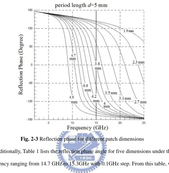
Fig. 2-3 shows the reflection phase angle versus frequency for various dimensions of the square patch. The vertical axis represents the reflection phase angle in degree and the horizontal is the operational frequency. The dielectric substrate employed is FR4 with relative dielectric constant 4.4 and thickness 0.8mm. The period is 5mm. From this figure, it is obvious to see that the reflection phase is zero degree at 15GHz for the case with patch dimension a=3.77mm. At 15GHz, the reflection phase angle deviates 0 degree as the patch dimension is varying. Such a simulation result reveals that we could manipulate the reflection phase angle by detuning the patch size. Notice that the phase angle difference against the patch size difference is nonlinear. It will
saturate as the patch dimension is greater than 4.9 mm or smaller than 1.9 mm.
Fig. 2-3 Reflection phase for different patch dimensions
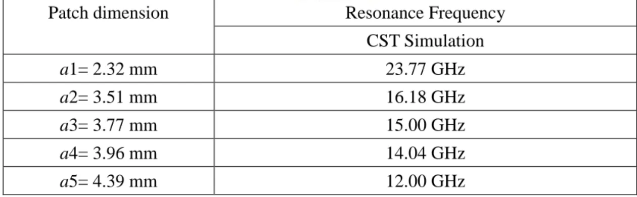
Additionally, Table 1 lists the reflection phase angle for five dimensions under the frequency ranging from 14.7 GHz to 15.3GHz with 0.1GHz step. From this table, we know that we could manipulate the reflected phase angle by adjusting the patch dimension. Significantly, as shown in this table, around 15GHz, they have the progressively phase delay angle about 70 degree.
Chapter 3 Numerical Simulation
3.1
Reflection characteristics of a gradient AMC surface
As was calculated in the previous section, the phase angle of the plane wave reflected by an AMC surface could be adjusted by varying the dimension of the square metal patch and was listed in Table 2. Therefore, we could alter the reflection phase angle distribution by adjusting the dimensions of the metal patches in the 2D array. For example, as shown in Fig.2-1, a square patches array was printed on a dielectric substrate backed with a metal ground plane. The periods along the x- and y- direction are the same and denoted as d. Notably, the size of the patch is varying along the x-axis; however, they maintain the same size along the y-direction. The dimensions of the square patches along the x-direction are respectively denoted as a1, a2, a3, a4, and a5. Such an AMC surface can provide a gradient phase angle
distribution along the x-axis; that is, they have a progress phase advance along the
x-axis, as shown in Fig.3-1.
Table 2 .Parameter Values of the Designed Structure
Parameters a1 a2 a3 a4 a5
Values 2.32 mm 3.51 mm 3.77 mm 3.96 mm 4.39 mm phase@15GHz 140° 70° 0° -70° -140°
Width of period : 5 mm Length of period : 5 mm
°Phase differences between adjacent cells : -70°
To understand the reflection characteristics of the gradient AMC surface, the full-wave simulation based on time-domain finite integration method (CST microwave studio) was employed for calculating the far-field scattering pattern. As shown in Fig.3-2, the gradient AMC surface was placed inside a rectangular box
equipped with absorbing boundary condition. The excitation is performed by a normally incident plane wave with the electric- and magnetic field along the y- and x- axis, respectively.
Figure 3-3(a) depicts the far-field scattering pattern over the x-z plane. Obviously, the reflection main beam is steered away from the normal incident direction. Additionally, some space left between the AMC surface and absorbing boundaries results in the existence of forward scattering. With the scattering pattern demonstrated above, it allows us to have an artificial surface able to redirect the incident wave to a desired direction. As will become clear later, the commonly used array antenna formula can be used to figure out the far-field scattering pattern.
(a) (b)
Fig. 3-3 Far field scattering pattern over the x-z plane with (a) 1 period (b) 2 periods (c) 3 periods (d) 6 periods along x-axis.
Besides, a periodic structure composed of several unit cells each of which is the gradient AMC surface shown previously was employed to calculate its scattering pattern. From Fig.3-3(a), (b), (c) and (d), we could observe that the reflection main-beam angle maintains and the beam-width is getting narrower with the increase in the unit cell number. Besides, the grating lobes are apparent in the periodic gradient AMC surfaces. Notably, due to the square unit cell as well as patch, both the polarizations can excite the progressive phase shift in the linear array; however, the reflection electric fields of the two cases are orthogonal to each other.
In addition to the far-field scattering pattern, we have calculated the reflection phase angle distribution on the plane with a distance 0.5 mm above the gradient AMC surface. As depicted in Fig.3-4, the horizontal axis represents the position along the x-axis indicated in the figure, while the vertical axis is the reflection phase angle in degree. Apparently, the reflection phase angle changes locally over each square patch. Significantly, the phase angles over the center position of each square patches respectively are -140, -70, 0, 70, 140. From the array antenna theory, an antenna array with the progressive phase delay angle could radiate its main beam angle toward a specific direction. This may explain the beam-steering characteristic of the reflection wave shown in Fig.3-3.
Fig.3-4 Electric field phase distribution along x-axis on gradient AMC surface
3.2 Array antenna factor
In the chapter 2, we have demonstrated the reflection phase angle versus frequency for various dimensions of square patch. Moreover, in the first section of chapter 3, the gradient AMC surface containing five dimensions of metal-patch array were organized to obtain the unique reflection characteristics shown previously. The full-wave simulation has been carried out for resolving the electromagnetic fields distribution. Specifically, the reflection phase distribution over the gradient AMC surface was obtained for proving that such a design can have the localized phase distribution. Consequently, a simple formula based on the array antenna factor is developed to provide a basic understanding for the steering of reflection waves.
Returning to the structure configuration shown in Fig.2-1, because of the uniformity in the electric field along the y-axis, we may consider it as a one-dimensional antenna array consisting of N elements with their j-th current
amplitude and phase separately denoted as Ij and j at the position x = xj. If the
coupling among the elements was neglected, the array factor contributing by the N elements can be written below.
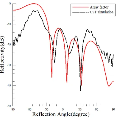
Figure 3-5 demonstrated the scattering pattern obtained by using full-wave analysis and the array factor formula given previously. It is interesting to observe that the array factor formula can predict the steering of the reflected wave. Notice that the array factor formula neglects the mutual coupling among antennas; therefore, the discrepancy between them can be observed.
Fig.3-5 Comparison between array factor calculation result and CST simulation result
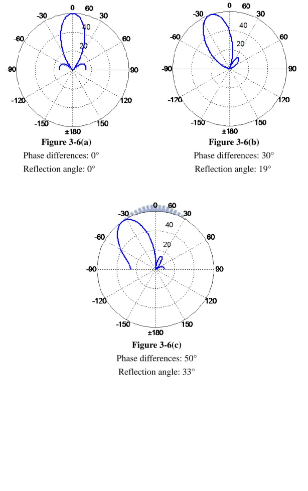
With the same phase differences between adjacent unit cells, the following Fig.3-6
AF
I
je
jje
jkoxjsincosj1
N
Figure 3-6(a) Figure 3-6(b)
Phase differences: 0° Phase differences: 30° Reflection angle: 0° Reflection angle: 19°
Figure 3-6(c)
Phase differences: 50° Reflection angle: 33°
Chapter 4 Experimental Studies
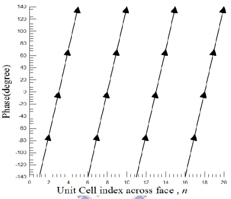
In order to increase the overall size of the AMC structure for higher gain reception, we repeat the period of phased array structure, as the following figure below.
Fig. 4-1 Linearly graded reflection phase from -140° to +140° with a 70° step along
the unit cell index at 15 GHz. By repeating the period of the phased array, we can obtain the larger structure with higher reflection gain.
In order to measure the far-field pattern for normal incident condition, we design a horn fixture by woods. By changing the distance between horn and the structure plate for 20 cm and 36 cm, we can figure out the field coverage issue in the following measurement. Our measurement frequency is about 14 GHz to 16 GHz, and the central frequency is at 15 GHz. By comparing the far-field pattern at different
Fig.4-2 Measurement set-up
4.1 Bistatic RCS Measurement
Fig.4-3 Bistatic RCS measurement schematic diagram
In bistatic RCS measurement, the transmitter horn rotates together with the tested structure, and the receiver horn is placed behind the transmitter by 4 meters away. After rotating around, the reflection pattern of the tested surface can be measured, as shown in figure 4-3 and 4-4.
4.2 Monostatic RCS Measurement
In monostatic RCS measurement, transmitter and receiver horn are all stationary away from the tested structure by 4 meters. When the structure rotates around, we can measure the far field reflection pattern not only for the specific face, but all around the structure. (Figure 4-5, 4-6)
Chapter 5 Numerical Results, Experimental Results and
Discussion
5.1 Numerical Results
The resonance frequency and the slope of phase-to- frequency curve (Fig.3-1) relate to four parameters: patch size, thickness of the substrate, dielectric constant and the unit cell dimension. By CST simulation, we will clearly know their relation between resonance frequency and these four parameters.
Patch Size
Generally, the larger patch size results in lower resonance frequency. As we can see in Table 3, the largest patch with a =4.39 mm has the lowest resonance frequency at 5
12 GHz; the smallest patch with a =2.32 mm has the highest resonance frequency at 1
almost 24 GHz in CST simulation. In figure 3-1, the curve with higher resonance frequency have smaller slope which indicates that it has more bandwidth.
Table 3 .Resonance frequency for CST simulation results against patch dimension
Patch dimension Resonance Frequency CST Simulation a1= 2.32 mm 23.77 GHz a2= 3.51 mm 16.18 GHz a3= 3.77 mm 15.00 GHz a4= 3.96 mm 14.04 GHz a5= 4.39 mm 12.00 GHz
Thickness of Substrate
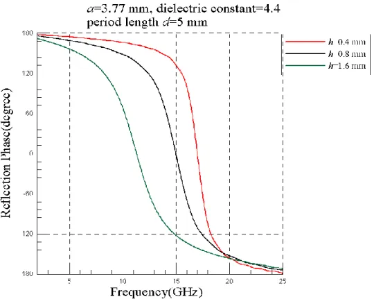
For simulation, we let a=3.77 mm, r=4.4, period size=5×5 mm^2.
Fig.5-1 .Reflection phase for different thickness of substrate, h =0.4, 0.8 and 1.6 mm.
Table 4 .Resonance frequency for CST simulation results against thickness
Thickness of Substrate Resonance Frequency CST Simulation
h=0.4 mm 17.01 GHz
h=0.8 mm 15.00 GHz
h=1.6 mm 11.31 GHz
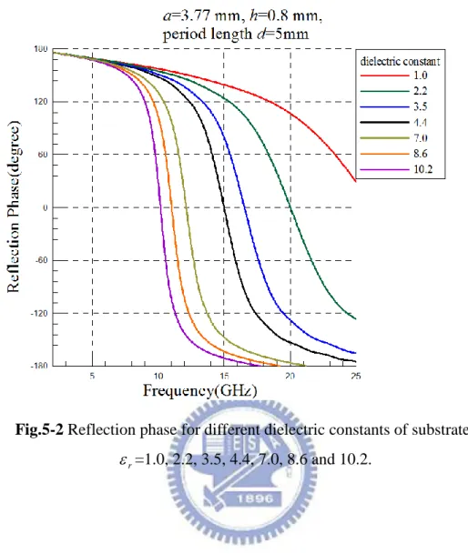
Dielectric Constant
We have known that the dielectric constant is proportional to the parallel plate capacitance. The Substrate with high dielectric constant leads to high Q in its equivalent resonance circuit, so the slope of curve in figure 5-2 becomes larger with smaller bandwidth, and vice versa.
Fig.5-2 Reflection phase for different dielectric constants of substrate,
r
=1.0, 2.2, 3.5, 4.4, 7.0, 8.6 and 10.2.
Table 5 .Resonance frequency for CST simulation results against dielectric constant
Dielectric Constant Resonance Frequency CST Simulation r =1.0 26.35 GHz r =2.2 20.03 GHz r =3.5 16.55 GHz r =4.4 15.00 GHz r =7.0 12.13 GHz r =8.6 11.02 GHz r =10.2 10.17 GHz
Unit Cell Dimension
In figure 5-3, we figure out that with larger unit cell dimension, the resonance frequency shifts to the higher frequency. On the contrary, with unit cell dimension smaller as d=3.8 mm, the resonance frequency shifts to the lower frequency. But the bandwidth changes slightly for different unit cell dimensions.
Fig.5-3 .Variation of reflection phase angle against unit cell dimensions.
5.2 Field Coverage
Electric field which the horn excites is not uniform to the far-field. In CST
Microwave Studio, the port we set as plane wave has uniform electric field. In order to simulate the actual situation, we draw a horn with the same size in the overall simulation. With a wave port excited, we will know the electric field distribution at any distance from the horn.
Fig.5-4 Electric field distribution at (a) 36 cm (b) 20 cm from the horn.
For distance 36 cm away from the horn, the uniform field coverage area is bigger than the one for 20 cm away. So that’s why the beam width of main beam for 36 cm away is a little smaller than the one for 20 cm. The comparison results between array factor calculation considering non-uniform electric field and CST simulation can be seen in figure 3-6.
5.3 Experimental Results
RCS reduction applications
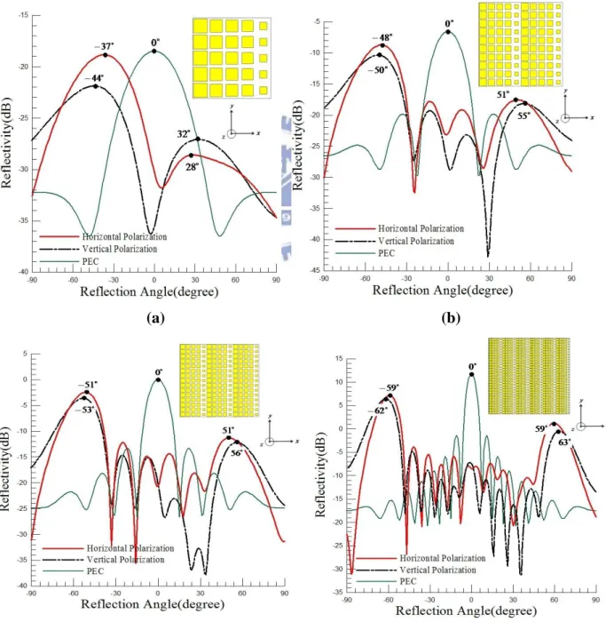
From the scattering characteristics depicted in chapter 3, we know that the gradient AMC surface can reflect the normally incident wave away from the incoming direction. Such a unique characteristic is promising for the application of RCS reduction. However, in the previous examples, the incident electric field is perpendicular to the surface gradient direction (defined as vertical polarization) as the symbol of arrow attached in the figure 5-5. To design a surface able to work properly for vertical- and horizontal- polarization, the orthogonal gradient surfaces were placed into the same structure as indicated in Fig. 5-5. Throughout this thesis, this structure will be named as supercell AMC surface.
Using the full-wave analysis, the scattering far-field pattern of the supercell structure illuminated by a normally incident plane wave (with electric field along the y-axis) was obtained and shown in Fig.5-6. When observing along the x-axis, the two major beams are contributed by the two head-to-head gradient surfaces located at the upper-left and lower-right ones. It is worthy of note that due to the square pattern in its unit cell the vertical polarization can also excite the two gradient surfaces at the upper-right and lower-left ones, generating the two major beams along the y-axis.
Fig.5-6 3D pattern of supercell AMC surface for CST simulation
In addition to the numerical calculation, we have also fabricated the supercell and measured its bistatic and monostatic reflections, respectively. The measurement was carried out in an electromagnetic chamber using the vector network analyzer and standard gain horn antennas. Before measuring the reflection characteristic of the supercell AMC surface, the scattering characteristic of the background (absorber reflectance) was first measured for identifying the scattering sources. Beside, the reflection characteristic of the equal size metal plate was measured as a reference to know the RCS reduction level for the gradient AMC surface in the normal direction. Figure 5-7(a), (b), (c), (d), (e), (f) respectively show the scattering far-field pattern for frequency operated at 14GHz, 14.5GHz, 15GHz, 15.5GHz, 15.8GHz, and 16GHz. The horizontal and vertical axes individually are reflection angle in degree and reflectivity in dB. The lines in red, black and green colors respectively represent the reflectivity of gradient AMC surface, PEC surface and background. Generally speaking, the gradient AMC surface can reflect the incoming wave away from the
evaluated within the 3dB beam width of the receiving horn antenna. In doing so, the RCS suppression rate for those frequencies respectively are 6.17, 8.07, 11.82, 18.53, 18.65 and 13.31 dB.
Fig.5-7(a)
Fig.5-7(e)
Additionally, the monostatic reflection of the gradient AMC surface was measured. It is apparently to observe that the reflectivity of the gradient AMC surface, in general, has more than 15 dB lower than that of the PEC surface. It means that the RCS
suppression rate using the gradient AMC is up to 15 dB.
Fig.5-8(c)
Conclusion
For this gradient AMC structure, the magnitude of the normal reflected wave can be completely reduced at the operation frequency. At this moment, the normal reflected wave magnitude is almost equal to the background which indicates that the reflected wave has been steered to the designed direction. This phenomenon is called Radar Cross Section (RCS) reduction, and we confirm it successfully by these measurements.
In this thesis, the reflection characteristic of a gradient AMC surface was investigated theoretically and experimentally. By adjusting the dimensions of the metal patches, we may obtain a surface with the progressively delay phase angle for reflecting the incoming wave away from the incident direction (normal incidence). Additionally, the orthogonal gradient AMC surfaces were organized periodically and put inside a supercell. Through the numerical and experimental studies, the excellent performance for RCS reduction in both horizontal- and vertical- polarization incidence conditions was found.
Chapter 6 Applications
Radar Cross Section applications are generally associated with military platforms, especially since it became fashionably known as stealth techniques, such as B-2 stealth bomber and F-117 stealth fighter of United States.
(a) (b)
Fig.6-1 (a) B-2 Stealth Bomber (b) F-117 Stealth Fighter
Generally, the speed camera on the road is operating at Ku, K, or Ka band. If we design an AMC structure operating at these bands and put it behind the car, then we won’t get the speeding tickets anymore, provided that the bandwidth of the structure can cover the whole bands we need. Although the current structure is limited by a narrow bandwidth, new design to improve the bandwidth is now in progress.
Using the simulation method in this thesis, we can design the AMC structure for RCS reduction or beam steering in any microwave band. Even in the visible light band, it is possible for us to design and fabricate by nanotechnology. This research will assist with the development of a flat reflector system characterized by its low cost, light weight, easy fabrication, and high tolerance to environmental resistances such as
References
[1] M. Paquay, J.C. Iriarte, I. Ederra, R. Gonzalo and P. de Maagt, ”Thin AMC Structure for Radar Cross-Section Reduction.” IEEE Trans. Antennas Propag., Vol.55, No.12, pp.3630-3638, Dec. 2007.
[2] D. Sievenpiper, L. Zhang, R. F. J. Broas, N. G. Alexopolus, and E. Yablonovitch, “High-impedance electromagnetic surfaces with a forbidden frequency band,” IEEE
Trans. Microwave Theory Tech., Vol.47, pp.2059-2074, Nov 1999.
[3] C. Mias and Jyh Haur Yap, “A varactor-tunable high impedance surface with a
resisiting-lumped-element biasing grid,” IEEE Trans. Antennas Propag., Vol.55, No.7, pp.1955-1962, July. 2007.
[4] D. F. Sievenpiper, J. H. Schaffner, H. J. Song, R. Y. Loo and G.
Tangonan, ”Two-dimensional beam steering using an electrically tunable impedance surface,” IEEE Trans. Antennas Propag., Vol.51, No.10,pp.2713-2722, Oct. 2003. [5] D. Sievenpiper, J. Schaffner, J. J. Lee and S. Livingston, “A steerable leakage wave
antenna using a tunable impedance ground plane,” IEEE Antenna and Wireless
Propagation Letters, Vol.1, pp.179-182, 2002.
[6] W. Yang, G. Hua and W. Hong, “Wideband artificial magnetic conductor structure for Ku-band antenna applications,” Microwave, Antenna, Propagation and EMC
Technologies for Wireless Communications, 2009 3rd IEEE International Symposium
on, Page. 954-957, 2009.
[7] Y. Y. Gu, W. X. Zhang, Z. C. Ge and Z. G. Liu, “Research on reflection phase characterizations of artificial magnetic conductors,” Microwave Conference
Proceedings, 2005. APMC 2005. Asia-Pacific Conference Proceedings, Vol.3,2005.
[8] M. E. de Cos, F. L. Heras and M. Franco, “Design of planar artificial magnetic conductor ground plane using frequency selective surfaces for frequencies below
1GHz,” IEEE Antenna and Wireless Propagation Letters, Vol.8, pp.951-954, 2009. [9] N. Engheta and R. W. Ziolkowski (2006). Metamaterials-Physics and Engineering
Explorations. The institute of Electrical and Electronics Engineers.
[10] J. Lanteri, C. Migliaccio, J. A. Laurinaho, M. Vaaja, J. Mallat and A. V. Raisanen, “Four-beam reflect-array antenna for mm-waves: design and tests in far-field and near-field ranges,” Antennas and Propagation, EuCAP 2009, 3rd European Conference on,pp.2532-2535, 2009.