國
立
交
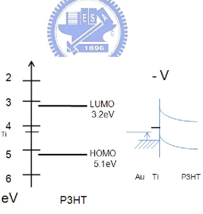
通
大
學
電機學院微電子奈米科技產業研發碩士班
碩
士
論
文
探 討 製 程 變 異 於 有 機 電 晶 體 之 影 響
Study of process variation on P3HT-Based OTFTs
研 究 生:陳猛飛
指導教授:簡昭欣 教授
探討製程變異於有機電晶體之影響
Study of process variation on of P3HT-Based OTFTs
研 究 生:陳猛飛 Student:Meng-Fei Chen
指導教授:簡昭欣 Advisor:Dr. Chao-Hsin Chien
國 立 交 通 大 學
電機學院微電子奈米科技產業研發碩士班
碩 士 論 文
A Thesis
Submitted to College of Electrical and Computer Engineering National Chiao Tung University
in partial Fulfillment of the Requirements for the Degree of
Master in
Industrial Technology R & D Master Program on Microelectronics and Nano Sciences
August 2008
Hsinchu, Taiwan, Republic of China
中華民國九十七年八月
i
探討製程變異於有機電晶體之影響
學生:陳猛飛 指導教授
:簡昭欣 博士
國立交通大學電機學院產業研發碩士班
摘
要
本論文研製之 P3HT 有機電晶體,是利用溶劑式製程方式,故須將其
粉末(溶質),經選用適當的溶劑與調配比例,使得
P3HT 能均勻得溶於溶劑
之中,再使用旋鍍製程方式,沉積形成
P3HT 薄膜 ; 此薄膜當成有機主動
層(
p-type),進而應用於有機電子相關產品。
P3HT 於有機材料中,被分類為共軛高分子;因具有自我組織的性質,而
形成高分子長鏈,因製程方式不同,所得實驗結果和薄片(lamella)排列也不
盡相同。經本論文實驗結果:首先藉由氯仿溶液與調配濃度百分比為 0.1%
之比例,能讓
P3HT 完全溶解於其中,不會因溶解度的關係而降低其效能;
相反的,利用二甲苯卻得到相對不理想之結果,因較差的溶解度關係所造
成。製程時,猜測搭配較少的比例與揮發慢的溶劑,可以提供相對較長排
列時間,使得微結構分子,有較恰當的排列方式,進而得到較高之結晶性,
而使的移動率相對的提高。接著探討不同規則區域性(Regioregularity_RR)
和分子量(Molecular weight),兩種溶質同樣溶於氯仿中,經電性與物性分析
結果,知道分子量差異比 RR 值來的重要。再經由 1500 轉速、烘烤(Curing)
溫度為 150℃與時間維持 3 分鐘下的製程條件,具有比較好的電性結果,這
也利用歐傑電子(Auger)和表面元素(ESCA)分析發現,氧分子含量都有相對
ii
比較低的情況,但是透過 FTIR,並無見到氧分子所造成的結果,猜測:其
的存在是利用物理吸附非鍵結,故無法被偵測到。
已知基本製程條件後,由於蕭特基接面會有較高的能位障產生,此位
能障位於金屬和有機物間,然而,藉由金(GOLD)的金屬材料和適當厚度的
附著層(Adhesion layer),可因功函數接近 HOMO 和其化學屬性的關係,得
到相對比較小阻值結果,另一方面,使用表面處理(HMDS),讓分子可更有
效排列與增加結晶性,而提高移動率與越接近零之起始電壓
(Threshold
Voltage)。
論文的最後,研究 P3HT 有機材料的穩定性,因為大氣環境對有機物來
說是一種挑戰。實驗結果顯示,製程而成的電晶體,卻在存放一個月左右,
即可明顯見到退化現象。可是再利用後段長壓退火,以通入氮氣方式,進
行 180℃和 30 分鐘的退火,可以有效改善效能,這樣的效果一樣可在低分
子量見到;同時發現,經過一連續製程步驟之元件,再經退火處理後,
On/off
比例值可達到 6~8x10
6次方,經由歐傑電子之縱深分析,適當退火可更有效
使氧分子被驅離出薄膜;可惜的是,移動率並沒有因此而提升和起始電壓有
往負值方向移動。最後利用定電壓和時間
STRESS 方式,發現只供給 Drain
-60 伏電壓下,P3HT 的 ID 電流,會隨時間上升而增加,且已達開啟電流,
此時,卻未發現閘極電流隨著上升的情形。但再次量測基本電性時,發現
整個
OFF 電流,受 STRESS 後,有上升趨勢,間接猜測是,因為氧分子,
經由
STRESS 時,再次進入薄膜,而可能導致的結果。
iii
Study of process variation on P3HT-Based OTFTs
student:Meng-Fei Chen Advisors:Dr.
Chao-Hsin Chien
Industrial Technology R & D Master Program of
Electrical and Computer Engineering College
National Chiao Tung University
ABSTRACT
A procedure is studying and using the solution-process to fabricate P3HT-based organic thin film transistor. Using appropriated solvent and weight percentage is needed. And then the P3HT solution will be spun and deposited to be as active layer for organic electronic.
P3HT organic material is to be classified to conjugated polymer. One of advantages is a property of self-organization and based on this structure to form a long chain. This long chain will be formed a lamella structure. If this lamella were packing closely, it would result a high regioregularity, which could obtain high mobility. Due to different process method, this lamella will be formed edge-on or face-on result. In my experiment, First of all, using chloroform to be a solvent with 0.1 weight percentages to fabricated OTFT can obtain better performance than xylene made, due to solubility and like dissolves like. Subsequently, we study the difference between regioregularity and molecular weight, two solutes were purchased from two different companies, dissolved them in the same solvent, chloroform. The result is that the difference of molecular weight is more importance than regioregularity. Moreover, fabricated by spin speed at 1500rpm and curing at 150℃ for 3 minutes can exhibit optimized result and in the meantime, observe that the oxygen concentration is less and less in the thin film analyzed by Auger electronic and ECSA surface elemental.
Known a basic process procedure, there is a Schottky barrier between metal and organic material resulting less the current transport. However, S/D deposited with gold and an appropriated adhesion layer can reduce this barrier height, due to their closest work function
iv
and surface chemical property. In addition to previous results, to use surface treatment (HMDS) is a good idea to improve the packing and ordering for strong chain interaction and lead to exhibit high mobility and approximate to VG=0 of threshold voltage.
In end of this thesis, we discuss about stability characteristics. Storage in the atmosphere, all of organic material will degrade as time goes by. This result is the same as P3HT polymer when it has been stored for one month. But the off current can be “healed” by annealing process at 180℃ for 30 minutes in furnace with N2 flow. Extra, low molecular weight comes to the same thing. Meanwhile, a device undergoing a serious process procedure can obtain a better performance, too. The on/off ratio is improved from 6x10⁴ to 8~6x10⁶; suspect that oxygen molecule can be driven off during annealing process. Unfortunately, the mobility is not to be improved and reduce down to 0.3x10⁻³ from 6x10⁻³ slightly and Vth is shifted to more negative, due to chain torsion. Last, constant voltage stress is applied to see how the drain current change. During stress, the drain increases with stress time going by when only drain electrode is applied at -60 voltages. There is no any gate current to be observed. We find out that the basic electrical result of the same device is changing after stress. A slight movement in off current, compared with just annealing one. So we suspect that the oxygen may diffuse into the film during stress.
v
Acknowledgement
I am so grateful to all of people who help in the preparation of this thesis. First of all, I would like to thank my serious and kindness advisor, Prof. Chao-Hsin Chien(簡昭
欣), for distinguishing right from wrong in reading paper, always pushing me to think
system and logical, discussion, and encourage opportunely. Without his advice, I will completely miss big picture in my research. He is best mentor one could possibly have.
Second, I would much appreciate my senior, Chia-Hao Chang(張家豪), for really helpful discussion and insights, sharing his considerable knowledge, presenting logically and giving a hand opportunely. His unfailing encouragement and enthusiasm are worth more to me than I can express. Also I owe thank for my classmates, 郭宇彥、陳弘森、詹
效諭、陳宣凱、江欣哲、林敬倫, no matter in my own lab or others, they are not only helped me to set up and prepare but also was always valuable for discussion from the first day joined the group. Thanks all senior, 鄭兆欽,楊明瑞, for guiding me a direction and sharing their insights.
Third, I am appreciated all related to people who working in NDL and NFC in NCTU, for their help in operating, troubleshooting, and dealing with administrate document when I used analyzed system. There is much experience that I missed and they are so kindness to assist with all of them.
Most of all, I want to thank my parents(陳元卿,鄭麗華) and sister(陳雪惠), for growing me up without any regrets. Without them, I could not have any thing. Finally, I also thanks for my “good friend”(蔡雨蓁) for staying with me, no matter what worse wind storm came to me.
vi
Contents
Abstract (Chinese) ………i
Abstract (English) ………iii
Acknowledgment………..v
Contents……….vi
Table list……….ix
Figure captions………..………..x
Chapter 1 Introduction 1.1 Overview of organic semiconductor……….………1
1.2 Conductor machination of conjugated polymer………3
1.3 Conjugated polymer of operation of OTFT………..4
1.4 Thesis organization………...6
Chapter 2 Synthetic effect in P3HT fabrication 2.1 Introduction and motivation………...10
2.2 Poly (3-hexylthiophene), P3HT-an organic semiconductor………...11
2.3 Fabrication process……….12
2.4 Different solvent, solubility and weight percentage………...…14
2.4.1 Results and discussion………...…14
2.4.2 Electrical results………15
2.4.3 Field effect mobility, on-off ratio and threshold voltage………..…18
2.5 Regioregularity and molecular weight………...20
2.6 Effect of various curing temperature……….….22
vii
2.6.2 Results and discussion..………...23
2.7 Effect of various curing time………26
2.7.1 Fabrication process………..26
2.7.2 Results and discussion……….…26
2.8 Effect of various spin-speed……….27
2.8.1 Fabrication process………..27
2.8.2 Results and discussion……….27
2.9 Summary………...28
Chapter 3 Surface treatment and contact resistance 3.1 Introduction and motivation……….53
3.2 Effect of the thickness of adhesion layer………..54
3.2.1 Fabrication process………..54
3.2.2 Results and discussion……….55
3.3 Surface treatment of silicon di-oxide gate dielectric………56
3.3.1 Fabrication process………..56
3.3.2 Results and discussion……….56
3.4 The ideal metal material………...58
3.4.1 Fabrication process………..58
3.4.2 Results and discussion……….58
3.5 Summary………...60
Chapter 4 Stability characteristics of P3HT OTFT 4.1 Introduction and motivation……….77
viii
4.3 Heat treatment: annealing process………79
4.3.1 Fabrication process………..79
4.3.2 Results and discussion……….80
4.4 Temperature dependence and constant voltage stress………...83
4.4.1 Temperature dependence……….83
4.4.2 Constant voltage stress……….85
4.5 Summary………87
Chapter 5 Conclusions and future work 5.1 Conclusion………..108
5.2 Future work………109
References………..………110
ix
Tables list
Chapter 1
Table 1-1 Common organic polymer………..……7
Chapter 2
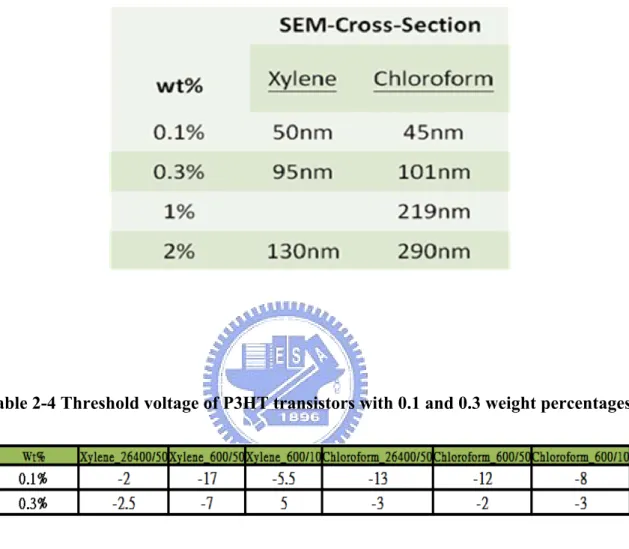
Table 2-1 Experimental table………..…...28 Table 2-2 Polarity of solvent and solute with the polarity……….28 Table 2-3 The thickness of P3HT transistors with different weight percentages
and solvents………..29 Table 2-4 Threshold voltage of P3HT transistors with 0.1 and 0.3 weight
percentages………29 Table 2-5 List of electrical parameter in different molecular weight………29
Chapter 3
Table 3-1 Electrical parameters of w/o and w/ surface treatment and operating in
linear and saturation region……….61 Table 3-2 Metal element and its work function, left, and Position set, right………61
Chapter 4
Table 4-1 Threshold value and On-off ratio value with samples stored one, two,
x
Figure captions
Chapter 1
Figure 1-1 The coupling and its connect method of the 3-substituted thiophene…………8 Figure 1-2 Steps of forming an energy band in Polyacetylene………8 Figure 1-3 Device structure of (a) bottom-contact and bottom-gate, (b) Top contact
and bottom-gate………9
Chapter 2
Figure 2-1 Poly (3-hexylthiophene) P3HT Chemical structure (a) monomer, (b)
Organization………30 Figure 2-2 P3HT Lamella (a) edge-on (b) face-on………..30 Figure 2-3 Fabrication process for bottom contact organic thin film transistors……….…31 Figure 2-4 Micrograph of bottom contact P3HT FET, (a) linear type (b) Finger-like…….32 Figure 2-5 Transfer characteristics of P3HT FETs spin-coated from different weight
percentages and solvents, (a) spin-coated from Xylene, (b) spin-coated from chloroform……….33 Figure 2-6 AFM synthetic result of P3HT in chloroform and xylene with different weight
percentages, (a) SiO2 and xylene 0.01wt%, (b) xylene 0.1wt% and chloroform 0.01wt%………...34 Figure 2-7 SEM cross-section of P3HT in chloroform FETs spin-coated from different
weight Percentages, (a) 0.1wt%, (b) 0.3wt%………..35 Figure 2-8 AFM topography of small scale scanning of P3HT in xylene with 0.01wt%, top, 0.1% middle and 2wt%, bottom………36
xi
Figure 2-9 AFM topography of small scale scanning of P3HT in chloroform with 0.1wt%, top, 0.1% middle and 2%wt%, bottom……….36 Figure 2-10 The output characteristics of typical device with different weight percentage
and solvents, (a) 600/50, (b) 26400/50 μm……….37 Figure 2-11 Output characteristics different with various weight percentages………….…38 Figure 2-12 The mobility of P3HT FETs with various weight percentages and solvents (a)
Field-effect mobility (b) On-Off ratio………39 Figure 2-13 The VT extraction using the linear extrapolation method for device operated in
the linear region (a) in saturation region (b) ………..40 Figure 2-14 Threshold voltage of P3HT FETs of with various weight percentages and
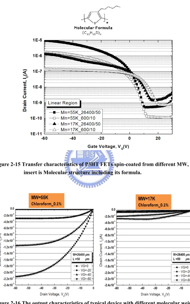
solvents………41 Figure 2-15 Transfer characteristics of P3HT FETs spin-coated from different MW, top
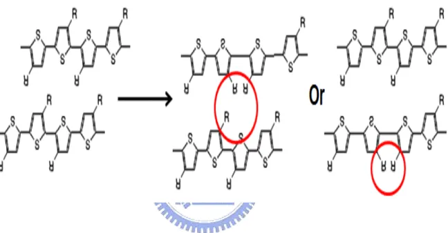
insert is Molecular structure including its formula……….42 Figure 2-16 The output characteristics of typical device with different molecular weight
MW=55K, left, MW=17K, right……….42 Figure 2-17 Transfer characteristics of P3HT FETs spin-coated from different curing
temperatures and solvents, (a) 600/50. A typical On-Off ratio versus the
temperature with vary dimension device (b) ………43 Figure 2-18 Atomic force morphology: 3D analysis from different curing temperature (a)
50℃, (b) 100 ℃(c) 150 ℃, (d) 200 ℃………..44 Figure 2-19 ESCA surface elemental analysis: elemental counts versus binding energy with various temperatures (a) Oxygen concentration………45 Figure 2-20 Electrical parameters: field-effect mobility of P3HT FETs with varies
dimension devices. (a) threshold voltage versus temperature (b) ………46 Figure 2-21 rr-P3HT molecular chain and its probability behavior of steric hindrance…..47
xii
Figure 2-22 P3HT FETs from different curing time and solvents (a) transfer characteristics (b) output characteristics………48 Figure 2-23 Auger depth analysis of PFETs compared with (a) curing for 3min (b) curing
for 15min………49 Figure 2-24 Transfer characteristics of different spin-speed with 0.3wt% in xylene and 0.1,
0.3wt% in chloroform including two different dimensions (a) 26400/50 (μm) and (b) 75/50 (μm) ………50 Figure 2-25 SEM cross-section of P3HT FETs spin speed at 3000rpm (a) xylene 0.3wt%
(b) chloroform 0.1wt%………51 Figure 2-26 Atomic force morphology: the morphology and 3D analysis from different spin
speed (a) transistor in xylene (d) transistor in chloroform………..52
Chapter 3
Figure 3-1 Scaling down issue in P3HT transistors (a) the mobility (b) the output
characteristic with different channel length………..62 Figure 3-2 Transfer characteristics of different Ti thickness with (a) Au metal,
(b) Pd metal………..63 Figure 3-3 Transfer characteristics of Ti only with different device dimension…………..64 Figure 3-4 Work function difference of Ti and band bending result………64 Figure 3-5 Transfer characteristics (a) w/ and w/o surface treatment, (b) the device
operates in the linear and saturation region w/ and w/o surface treatment…….65 Figure 3-6 The molecular ordering and packing way (a) w/o and (b) w/ surface treatment.66 Figure 3-7 The theory of surface treatment of HMDS from hydrophilic to hydrophobic
surface……….67 Figure 3-8 Contact angle value on surface of silicon di-oxide (a) water, and (b) ethylene
xiii
glycol………..67 Figure 3-9 AFM surface roughness of w/o, top, and w/, bottom, surface treatment………68 Figure 3-10 Gate leakage current characteristics of typical device w/ and w/o surface
treatment………..68 Figure 3-11 Typical electrical characteristic w/ and w/o surface treatment (a) the
extraction of the mobility (b) threshold voltage with all device dimensions…69 Figure 3-12 Transfer characteristics with different S/D metal (a) W/L=26400/50,
(b) W/L=75/50………70 Figure 3-13 Transfer characteristics with different S/D metal (a) W/L=26400/50,
(b) W/L=600/10………...71 Figure 3-14 Electrical characteristics with different S/D metal (a) the mobility,
(b) threshold voltage………...72 Figure 3-15 AFM: 3D analysis, P3HT film on channel and metal, respectively, (a) Au,
(b) Pd………...73 Figure 3-16 The output characteristic result compared with Au and Pd metal. (a)
W/L=26400/50, (b) W/L=600/10 in linear region……….74 Figure 3-17 High hill-like regions between metal and organic interface. (a) SEM,
(b) AFM………..75 Figure 3-18 Gate leakage current characteristics of typical device with different metal
materials……….76 Figure 3-19 The transfer characteristics of P3HT FETs with different metal materials……76
Chapter 4
Figure 4-1 The transfer characteristics of PFETs after fabrication and samples stored one, two, three months later………..89
xiv
Figure 4-2 The variation of electrical parameters of PFETs after fabrication and samples stored one, two, three months later………..89 Figure 4-3 The variation of electrical parameters of PFETs after fabrication and samples
stored one, two, three months later………..90 Figure 4-4 The transfer characteristics of PFETs with annealing process in a range from
50℃~250℃……….90 Figure 4-5 The mobility of PFETs with annealing process including vary annealing
temperature………91 Figure 4-6 AFM multi-analysis of morphology(top left), phase, image statistics and section
curve (a) un-annealing, (b) annealing at 50℃, (c) annealing at 150℃, (d)
annealing at 250℃………92 Figure 4-7 The transfer characteristics of PFETs after annealing process for 30min and 3hr
(a), electrical parameter of On-off ratio, comparison of w/o and w/ annealing process………...93 Figure 4-8 The mobility of PFETs compared with before and after annealing process for
30min (a), electrical parameter of Vth, comparison of before and after annealing process (b) ………94 Figure 4-9 ESCA of PFETs compared with before and after annealing process for 30min
and 3hr………..95 Figure 4-10 Auger depth analysis of PFETs compared with before annealing (a) and after
annealing process for 30min and 3hr (b) ………...96 Figure 4-11 The output characteristics of typical device, (a) before annealing, (b) after
annealing for 30min………97 Figure 4-12 Gate leakage current characteristics of typical device with before annealing, and
xv
Figure 4-13 The transfer characteristics of typical device with an average of before
annealing, and after annealing for 30min and 3 hr……….98 Figure 4-14 The output characteristics with stored device and low molecule comparison of
before annealing and after annealing for 30min (a), skip curing and go
annealing directly (b) ………..99 Figure 4-15 The transfer characteristics with various temperature measurements (a) before
annealing, (b) after annealing………100 Figure 4-16 The electrical characteristics of on-off ratio versus various temperature
measurements (a) before annealing, (b) after annealing………101 Figure 4-17 The electrical characteristics of mobility versus various temperature
measurements (a) before annealing, (b) after annealing………102 Figure 4-18 The electrical characteristics of Vth versus various temperature measurements
(a) before annealing, (b) after annealing………103 Figure 4-19 Constant voltage stress versus time measurement (a) varies terminal voltage
stress, (b) the transfer characteristics. Top insert is varying terminal………104 Figure 4-20 The gate current as function of stress time, (a) VG=-20V and VS=VD=0V, (b)
VG=VS=0V and VD=-60V………105 Figure 4-20 The gate current as function of stress time, (c) VG=10V and VS=VD= -60V,
(d) VG=0V and VD=VS= -60V(continued) ………106 Figure 4-21 Constant voltage stress versus time measurement of comparison of before
- 1 -
Chapter 1
Introduction and motivation
1.1 Overview of organic semiconductor
Organic thin-film transistors based on solution-processed and semiconducting conjugated polymers have highly promising and feature technological properties, due to its high mobility. Polymer, it also follows in complex microstructures. Indeed, using solution-processed process is one of method to suppress cost, cohering with the low cost requirement, and simple process procedure. For application, it can apply to large area, flexible panel, flat-panel display, and identification tags [1.1] [1.2] [1.3].
In the early 1970, the conducting conjugated polymer has known as polyacetylene, PA, with it repeat unit (C2H2) n and announcement [1.4]. It is one class of conjugated polymer, which consists of the hydrocarbon. After doping appropriated oxygen (oxidation), its conductivity was reached to 103 S/cm, compared with un-doped one. Table 1-1 shows common organic polymer. What a great history. The theory of transporting is that the charge is transporting (hopping) along main chain, which is composed of sequences of alternating single (named sigma bond) and double bond (pi bond). Those bonds are composed of outer value electron between atoms or between atoms and other covalent bond, which sharing of pairs of electrons. The pi bond, which electron could gathers around mostly, can provide a conductive path to let the carrier “move”. Greatest thanks for those inventors. They were awarded the Noble Prize for this contribution. General speaking, There are many methods to changing the conductivity such as electropolymerization and By now, by such investigated result it appealingly make many researches join in, improve its chemical properties, and many study result were published. The disadvantage of PA is unstable when it exposes in the atmosphere, due to the moisture and humidity so that its value of existence should be
- 2 -
concerned.
Polythiophene is one of extended conjugated polymer by using a concept of polyacetylene. Replacing of benzene with sulfuric acid provided. Due to its conductivity and electroactivity, in the past two decades, Polythiophene is known for its environmental stability, structural versatility, and combination of original electronic properties [1.5]. Controlling structural regularity for improving high electrical conductivity is major problem. The result of finest optimized electrochemical synthesis is quest for. A analysis through optical properties of polymer and the electrochemical have illustrated that the conductivity increase with decreasing band gap from 2.20 to 1.90 eV [1.6].
In 1985, R. L. Elsenbaumer et al [1.7] reported that they were subsubstituted at beta position of a monomer of thiophene to 3-alkylthiophene and then using a method of chemical or electrochemical, like AuCl3 or FeCl3 …etc to copolymerize to poly-3-alkylthiophene (P3AT). This exhibits a conductor and optical property and it can be dissolved in organic solvents at room temperature. It is easy to form a thin film. This P3AT also exhibits a good stability.
P3AT is a typical polymer with a result of regioregularity, which improves the property of polythiophene. Due to 3-alkylthiophene is dissymmetry, leading to three types of dyad structure as head-to-tail, head-to-head, and tail-to-tail isomers, as shown in Fig. 1-1[1.8]. the fact of asymmetry is that both the α-position of oxidation potential and the difference betweenα- and D-position will decrease as the number of ring boosting. HH coupling structure is undesired because of steric hindrance, which is based on van der Waals force (discuss in chapter 2). This kind of steric hindrance makes a random chain packing and interaction, causing unstable conjugated system and low chain length. Side chain, alkyl, impede packing in solid state. In contract, HT coupling will reflect to self-organization and obtain a better ordering. Ordering will affect packing. Notice that short-range attraction in the interaction will appear anisotropic, when they pack themselves. Because lowest packing potential energy will be in regular arrangement, local chain will show as orientation dependent [1.9]. Some researchers are effort to produce high regioregularity by 2, 5-linked
- 3 -
repeat unit such as McCullough et al. [1.10] and Rieke et al. [1.11]. Of course, the other position substituted like 2, 4- and 2, 3-coupling resulted in a problem of steric hindrance.
For 3-alkylthiophenes and other 3-substituted monomers, the observed effects were electrosynthesis conditions. There are so many ways to obtain HT-PATs. Notice that Polythiophene itself could not be dissolved, and the reason for substituted alkyl side chain is to make it soluble.
1.2 Conducting mechanize of conjugated polymer
Although this conducting theory is not clear, it is known that they are insulator or weak conductor of semiconductor as its natural. The molecular structure can be formed by atomic, which bind by covalent bond. Many interchain of molecules are bonded together by chemical bond, like van der Waals force with smaller than 10 kcal mol-1. A long chain composed of each single molecule is monomer and there are hounded or thousand in a chain. After doping, meaning remove or inject electron, it will become a conductor or semiconductor. Therefore, it can explain by a theory of the classical semiconductor of band structure. The number of molecular orbital will increase with the number of atomic bonding to molecule. When these many orbital are spaced together, they will form a continue energy band. For instance, Polyacetylene [1.12] as degree of polymerization increase, the π and π* orbital of CH will accumulate successively, energy distance between two neighbor orbits of different molecules is closing (overlapping) and finally, forms a energy band as shown in Fig. 1-2.
At the equilibrium, the highest occupied molecular orbital is named HOMO and the lowest unoccupied molecular orbital is named LUMO. There are similar as conducting band and valence band. The bandgap energy Eg between the bottom of LUMO band and the top of HOMO band is the width of forbidden energy gap. General speaking, in traditional material, it regard the band gap within 0eV, no gap, as a conductor, insulators are characterized by a large
- 4 -
bandgap and the bandgap of conjugated polymer is around 1~3.5eV and that is a reason for organic semiconductor.
The feature of conjugated polymer is that the polymer chain is composed of many monomers by covalent bond. Secondary covalent bond are named π-bond, which is composed of carbon-carbon of single- and double bond with interacting each other and above π electron orbits the charge can travel along major chain or hopping to neighbor orbits for transport. The mobility can be obtained by this phenomenon. When the distance of carbon and carbon in main chain is the same, the π-electron is to be delocalized completely and then the band gap will be shorter and increase conductive. If the π-electron were delocalized as possible, it would reduce the band gap between conductor band and valence band. So far, the best way is adding a substitute radical in main chain to pull or add electron. The experimental results illustrate that it not only shorts the bond length between molecules, but also increase the feature of double bond [1.13][1.14]. Because the observed polycrystalline is studied, traps will attribute to defects and grain boundaries and dominate the transport.
1.3 Conjugated polymer of operation of thin-film transistor
The are several methods to deposit organic semiconductor of P3HT such as dip coating, speed-coating, drop coating, and print process [1.15]. Recently, the solution-process P3HT can be deposited by vacuum evaporation [1.16], like small polymer. OTFT device performance can be affected by controlling external process procedure, like deposit rate and temperature. These results will reflect to morphology and electrical result. Post-deposition treatments, such as annealing and capping a protect layer, also preserve and improve molecular ordering, respectively. In this thesis, we use solution-process to deposit P3HT thin film onto SiO2 surface and the device structure is bottom gate and bottom contact, as shown
- 5 -
in Fig. 1-3 (b). Because of less step of lithographic and prevent organic will be affected by metal evaporating step. Figure 1-3(a) shows a bottom-gate and top contact structure, which report a better performance for limitation of organic materials. Of course, all of them have own advantage and disadvantage and within the basic MOSFET architecture.
Basically, the structure is a three-terminal device, where a voltage applied at gate electrode to adjust current flow, source contact is used as the voltage reference, and drain electrode will operate device in linear region (small voltage) and saturation region (larger VDS). There are several situation of operation, for instance, p-type semiconductor will be demonstrated. First, all three electrode are applied a zero voltage. The charge in semiconductor is in thermal equilibrium and there are no current. Second, A positive voltage is applied at gate electrode, the electron in the semiconductor will be induced and move to the interface of semiconductor and insulator. This situation is called depletion region. The width of depletion region, Wd, can be calculated by an equation below,
(1-1)
Where NA is the charge carrier density and εs is the permittivity of the semiconductor
[1.17]. Third, the accumulation region is form by applied a negative gate biased. Induced
charge is hole carrier, which treated as transporting carrier and forming channel path. And also, the drain voltage is also applied. The current starts flow from source to drain. There are uniform charges per unit area in the channel. When the gate voltage increases the proportioned current will be obtain. Fourth, the drain voltage is applied only, the gate a voltage difference will become positive, and then a depletion region will be formed.
- 6 -
1.4 Organization of this thesis
In my thesis of organization, I hope states reasonable and logically.
a.) Chapter two: we describe about solvent related to solubility and polarity. Because we are used solution-process throughout all my experiment, solvent study is needed. Next, electrical result can be related to solvent and weight percentage directly. We also pick up one optimized term to discuss next chapter. Organic is temperature-dependent material, because of its chemistry properties. The effect of the glass transits temperature and the melting point is a factor for concerning. So how many times and temperature are needed when the molecular can interact and order each other by thermal diffusion.
b.) Chapter three: A study of metal material, its chemical property and work function difference, is discussed. The thickness of an adhesion layer, different metal material and surface treatment, they are all objection we investigate.
c.) Chapter four: stability is a challenge for organic material, due to air and temperature are most impact and very sensitive in the device. What kind of elemental in air could affect it? We need to know and deal with that problem.
d.) Chapter five: the conclusion and future work will be involved.
Description of analyzed result above is supported by physical analysis as far as possible.
- 7 -
Table 1-1 Common organic polymer
- 8 -
Figure 1-1 The coupling and its connect method of the 3-substituted thiophene [1.8].
- 9 -
Figure 1-3 Device structure of (a) bottom-contact and bottom-gate, (b) Top contact and bottom-gate.
- 10 -
Chapter 2
Synthetic effect in P3HT fabrication
2.1 Introduction and motivation
Organic thin-film transistors based on solution-processed, semiconducting conjugated polymers have highly promising technological properties, resulting in complex microstructures.
The P3HT transistor is easily affected by intrinsic and external factors such as regioregularity, molecular weight, solvent, temperature, and many related process factors, leading to different result of electrical parameter and chemical property. For instance, from solvent point of view, besides the evaporate rate will affect crystalline [2.1]; the solubility is also an index for soluble conjugate polymer in liquid. The reason can be explained that new binding force is high enough to attacks old one, make molecular interaction break, so that the solute can be dissolved well. Another relation of solution process with solution adjustment is the weight percentage. The weight percentage is not only related to supersaturation of solvent itself but also it has a viscosity, which will reflect the thickness of thin film obviously [2.2].
From the molecular weight of view, the variation of molecular weight follows a morphology and phase. Many labs are observed the mobility value differently and accuse for this factor. Its molecular weight with mobility values increasing from 1.7x10⁻⁶ to 9.4x10⁻³ cm2 V-1S-1[2.3] [2.4]. But there is a curious thing; MW can be obtained by different solvent. It
seems lose the base line of experiment. And all of external process effects include curing time, curing temperature and speed spin…etc. During curing process, many factors are involved. Those factors from molecular interaction to each segment of chain reaction are important for transporting and further affect in device performance. Of course, the device as quenched to room temperature is another important thing.
We present here a study of related to upper description from solution adjustment to the difference of MW, try to explain each result systematically from theory to physical property, and all related investigation will be illustrated by electrical and physical analysis. We also try to develop the optimized terms.
- 11 -
2.2 Poly (3-Hexylthiophene), P3HT – an organic semiconductor
For this thesis work, the organic semiconductor utilized as active layer was poly (3-Hexylthiophene) (P3HT) with its repeat unit (C10H18S)n. It is based on the polythiophene, aromatic compound, and the alkyl group, hexylkyl, take replace and incorporated into a polymer chain of 3-position. The molecular formula of P3HT represents (C10H18S) n; C, H, S represents carbon, hydrogen, and sulfur, respectively. “n” is represented a repeat unit, as shown in Fig. 2-1 (a) [2.5]. Two P3HT radicals can be incorporated into a polymer chain by a forming covalent bond. Due to side chain and sulfur, the self-organization is asymmetry, leading to Head-to-head (the position of covalent is 2-5) coupling and another is head-to-tail (the position of covalent is 2-2) coupling. In Fig. 2-1(b), they are composed of one single radical and others, resulting to two type of result, regio-regular and regio-random. A region-random of P3HT is consisting of head-to-head and tail-to-tail in coupling and a region-regular is only consisting of head-to-tail in coupling. The value of region-regular can be calculated by equation [2.6]:
(2-1)
Where HT is a value of head-to-tail, and HH is head-to-head. High regioregularity means that the couple of forming type is mostly like head-to-tail. In this type, it can obtain high crystalline and ordering, due to regularity of molecular structure make molecular chain fit into the crystal lattice. Thus, the transporting carrier moved in π system along main chain, due to molecular orbital (electron cloud) is easy and increases a probability of intramolecular mobility. The coupling of head-to-tail can be more stabilizer than head-to-head one, because side chain of head-to-head structure may too close to make chain torsion and low chain conjugated length or unfavorable coplanarity. The transport will be interrupted along main chain and low the value of mobility. By different sublimed or purity process method, the different rr-P3HT value can be obtained, for instance, following the McCullough rout, P3HT with regioregularity of 91% and 95% was obtained. Or the sample of highest regioregularity was 96% HT, synthesized by the Rieke rout [2.7]. Indeed, many researches in this field with different regioregularity have a relative to the mobility.- 12 -
two-dimensional conjugated sheets formed by interchain stacking [2.8]. In figure 2-2, the lamella has two type of lying ways onto the substrate, edge-on and face-on, respectively. It depends on the process methods (drip-casting or spin-casting). X-Ray Diffraction (XRD) studies are also supported. It synthesized that organic thin film transistors made with 81% head-to-tail P3HT by spun from chloroform had mobilities in the range of around 10-5 to 10-4 cm2 V-1s-1. Contrariously, highly head-to-tail value of 91% had mobilities around 10-2 to 10-1 cm2 V-1s-1. The result is responsible for the structural order in the polymer layer. For instance, high density of packing and ordering will increase the hopping opportunity to neighbor chain. Moreover, X-ray studies show that layer as spun at lower speed or drip-casting from highly rr-P3HT value exhibited an orientation order of the lamella with edge-on to the substrate and the direction of pi-pi stacking is in perpendicular to substrate. In contrast, the film as spun with high speed with low region-regularity P3HT (81%) has parallel the substrate and its pi-pi system is perpendicular to substrate. They are opposed to each other.
Before a lamella of polymer chain forms, the conformation order of molecule about rotation may occur at a single bond. This phenomenon is due to thermal energy provides and the material itself has lower rotational barriers, making the chains flexible so that polymer molecular can rotate all the time.
In our experiment, P3HT thin films are deposited by spin costing in the environment of atmosphere. Before it spun onto substrate, it needs to be dissolved. There are two different solutions in this experiment, chloroform and xylene.
2.3 Fabrication Process
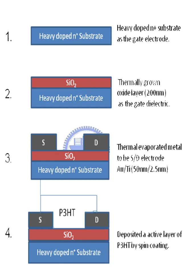
The standard baseline process for fabricating P3HT thin film transistors in this thesis is described below. The substrate in this work was n++ silicon, although FETs were also successfully fabricated on the flexible or glass substrate.
The steps of process flow are shown in the Fig. 2-3 and are described in detail below: 1. Silicon wafers are cleaned through RCA standard process, and this n++ silicon
substrate (0.002~0.004Ω-cm) act as gate electrode.
2. Silicon di-oxide is deposited by APCVD Wet-Oxidation. This thermal oxidation SiO2 remains at 980℃ in the deposition chamber. The thickness is around
- 13 -
200nm, which measured by n&K system.
3. Gold Source/drain electrodes are defined on the photo resist-coated (FH6400L) dielectric by lithography by electron beam deposition. Titanium (Ti) is used to be an adhesion (sticking) layer for firmly sticking gold and dielectric. And then photoresist (P.R.) will be removed by life-off process in acetone with vibrations in ultrasonic for 5min.
4. Poly (3-hexylthiophene), P3HT is spun onto gate dielectric and S/D electrodes. The substrate remains at room temperature during deposition. Typical background process of solution is described,
A.) P3HT solute will be dissolved by xylene and chloroform, respectively. Weight percentages are classed as 0.01wt%, 0.05wt%, 0.1wt%, 0.3wt%, 1wt%, and 2wt%.
B.) All solutions were filtered through a 0.20 μm pore-size PTFE membrane syringe filter before use.
C.) For spin coating, the film is deposited from solution by two kind of spin rate: first, at a spin rate of 500rpm for 10s (for uniformity);
second, at spin rate of 1500rpm for 25s (for thickness).
D.) All samples will be curing on hot plate at 150℃ for 3min, and quench to room temperature in air.
Upper experimental terms are summarized in Table 1-1 experimental table for reference. Before the active layer of P3HT is deposited, all samples are cleaned by soaking in acetone with vibrations in supersonic oscillator for 5min. the reason for this is removing the residual organic and particle contaminants on the channel region.
A typical FET pattern is shown in Fig.2-4. Involved channel width/length are 75/50, 600/50, and 26400/50 (μm/μm), respectively. There are two kinds of layouts used in fabrication of P3HT FETs, linear-like and figure-like. The channel length of linear-liked are in a range of 10~100μm, and the width are in a range of 75~3700μm. The channel length and width of finger-liked is fixed at 50μm and 26400μm.
All of electrical measurements and extraction were performed using an HP4156 semiconductor parameter analyzer, which was set in a shield box in atmosphere. The surface morphology of P3HT transistor was observed by atomic force microscope (AFM), device cross sections were observed by scanning electron microscopy (SEM).
- 14 -
Aldrich Chemical Company (MW=17K, RR>98.5%). Different regioregularity and molecular weight will be discussed later.
2.4 Different solvents, solubility and weight percentage
2.4.1 Result and discuss
Initially, there are so many P3HT precipitations in xylene solvent when it is dissolved to be a solution and the same situation is observed in chloroform with weight percentage higher than 1wt%. The solute of P3HT can be dissolved in chloroform easily, whereas xylene had poor solubility. Further, solvents and solutions will be gelled, although it is reported that both of them can dissolve P3HT solute. Two likelihood reasons for this are that “supersaturation” and “like dissolves like”.
For supersaturation, this explanation is based on fundamental chemical. It defines that contains more of the dissolved material than could be dissolved by the solvent under normal circumstances, meaning each of solution has its supersaturation nearly. If the proportion of solute is lower a level, solvent could dissolve them easily. Thereagainst, if the proportion of solute is beyond, it would not easy to dissolve.
For like dissolves like, it is related to polarity. Polar compounds dissolve in polar compounds and non-polar dissolve in non-polar. The types of intermolecular forces dictate these results. Moreover solution is a homogeneous physical mixture of solvent and solute. The solute particle sizes are ions, atoms, molecules or small combinations of these units. Basically, polarity of material compounds are decided by polarity of molecules and polarity of molecules are responsible for its polarity of bonds. Let us start off the solvent. Chloroform (CHCl3) has 3 bonds with chlorine (two of them symmetrical; see Table 2-2), and one with hydrogen. Chlorine, like many of its neighbors on the right side of the periodic table, is very electronegative: it pulls electrons towards its nucleus, like so:
- 15 -
C---Cl
+
-Positive pole Negative pole
Thus, it is a polar bond. The two symmetrical chlorine-carbon bonds "balance out" this pulling, so that no net pull occurs. The remaining chlorine-carbon bond is not "balanced out" by the less-polar hydrogen-carbon bond, resulting in a net polarity, with the "-" end towards the chlorine atom. Xylene (Paraxylene, C8H10 (C6H4C2H6)) is low-polarity [2.9]. Although the side chain is less-polar (C is negative pole and H is positive pole), they are located at each side. According to this result, the polar of CH3 bonds balance out and its polarity is low.
At room temperature, xylene solution will gel within a few minutes. In addition, when devices were fabricated in xylene and exceeded 0.3wt%, the solution was not easy to pass through a 0.20 μm pore-size PTFE membrane, due to precipitation should block. About chloroform, it will dry out within several weeks, depending on low wt% ratio.
The ratio of weight percentage was defined as:
wt% = (grams solute / grams solution) X 100%
(2-2)
There are two equations for calculating weight percentage, but their results are the same.2.4.2 Electrical results
A set of transistors was fabricated with different weight percentages. Each new transistor set was measured and added to the plot in following figures. Although there is a vibration across these devices, the trend of measured result is stable fairly.
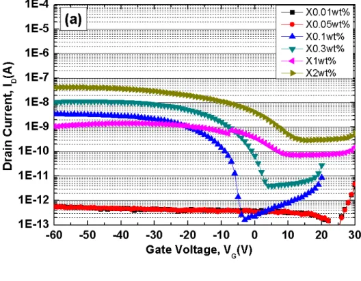
Figure 2-5 shows the transfer characteristic of P3HT transistors from different weight percentages and solvents. For P3HT in xylene, as you can seen in Fig. 2-5 (a), the result of 0.01wt% and 0.05wt% indicates that the data it is near a limit of measured machine, so a obtained curve may not be true, and there is no yield within 0.05wt% when measure. We
- 16 -
suspect that thin film is not to be formed so that obtained result is poor. In figure 2-6 (a), AFM surface morphology illustrates that the roughness of P3HT transistor in xylene with 0.01%wt is close to SiO2 one. For 0.1wt% in xylene and 0.01wt% in chloroform as shown in
Fig. 2-6 (b), the surface morphology reaches around 3.5nm. It indicates that the roughness of
exhibited performance is around 3 nm, but the roughness of xylene with 0.01wt% is below that. In addition to phase data, our think, thin film forming should be an issue.
Low weight percentage, 0.1wt% and 0.3wt%, the device turn on approximately at Vg=0. In chloroform devices, as shown in Fig. 2-5(b), lower weight percentage exhibits the same condition, except 0.01wt% and 0.05wt%, and they exhibit a similar curve to 0.1wt%. Despite their result are closed to 0.1wt%, but it is not good enough for on current. As following P3HT in both solvent with weight percentage increasing, the turn-on voltage is shifted toward to positive values. In other words, the off-current is increasing when weight percentage boots. Two possible reasons for this condition are that first, the precipitation and impurity more and more in active layer with high weight percentage could exhibit a defect, when the solvent reach its own supersaturation.
Second, weight percentage can be affected by the viscosity so that the thickness is an index for supporting this result. As you observed in figure 2-7, indeed, the thickness increases with weight percentage rising (the rest of part of thickness, P3HT in xylene and chloroform, please refer to Table 2-3). It could involve more the number of defects in the film. Additionally, those defects can act as trap center, and transport carrier will be trapped during the device operating in accumulation region. Trapped carrier will be released by applied a reverse voltage.
About on-current, it increases with weight percentages booting clearly. Figure 2-8 shows the surface morphology, which scanning by AFM. P3HT transistor in xylene observed a clear line-like structure onto the SiO2 after spun. The line-like structure, named nanofibrillar, is
- 17 -
consisted of nano-rod. This nano-rod is relative to ligands, which is control agent. The component will affect growth of nanorod. Apparent result also observed with 2 weight percentage. We suspect that the P3HT thin film is a long-chain polymer with lamella layer structure. The carrier is transferring through pi bond, which located at above sigma bond, and also it is source of electrons cloud. With 2 weight percentage, there is a possible chance to form a clear and long line. In contract, less weight percentage, like 0.1wt%, cannot form that. The result agrees from the data published by Yang et al. [2.10], who explains that long nonafibrils are composed of nanorods with width of ~22nm. He also suggests that all of long nanofibrils exists grain and grain boundaries. On the other hand, these grain and grain boundaries can be a trapping and releasing center so that affects the result of off current further.
Nanofibrillar provide a conductive path, and transfer carrier can go through it easily. Also it improves a chance of hopping transfer. Surprisingly, this data has not agreed with P3HT transistor in chloroform, as shown in Fig. 2-9. Nanofibrils are not clearly and even short in sample of 2 weight percentage, compared with samples in xylene. In contrast, in low weight percentage sample, nanofibrillar is to be formed, due to its boiling points. Xylene solvent has high boiling point around 138~139℃, and about chloroform, it is around 60.5~61.5℃ (obtained from the MSDS of Aldrich-sigma company).
Many researches group [2.11] [2.12] reported that the elongated nanocrystals are strongly affected by solvent-evaporation rates and costing solvents. This is due to its low boiling point and rapid evaporation speed. For high weight percentage in our study, it is not enough time to interact and self-aggregation in molecule before P3HT dry out. This results a short nanofibrillar on SiO2 surface. For low weight percentage, it is probably that small number of molecule with semidry situation could self-organize to form the thermodynamic structure and efficiently to form nanofibrillar by nano-rod.
- 18 -
In fact, one more suspect is that higher weight percentage can obtain thicker film. General speaking; a solvent will be dried out from outer (surface of a film). Self-organization inward film is on progressing when the surfaces of organic film dry out. So based on this reason, it may understand that on current increases with higher weight percentages.
Figure 2-10 shows the output characteristics of typical device with different weight
percentage and solvents. The P3HT transistors show MOSFET-like characteristics, and they are obtained for negative bias. It indicates that P3HT behaves as p-type semiconductor. For small negative source-drain voltage (VSD) the FET operates in the linear region, and observed from result shows an ohmic contact. When the source-drain voltage increases, the gate field is no longer uniform, and accumulation area is formed. Beyond a certain VSD, the current becomes saturated. The shape of I-V curves are identical, but the magnitude is quite difference. Let the output characteristics of chloroform values minus xylene ones and the result shows in Fig. 2-11. It is indicated that the performance of P3HT field effect transistor in chloroform has a better result than that in xylene ones, and no matter what weight percentages, P3HT transistors dissolved in chloroform obtained the same result.
2.4.3 Field effect mobility, on-off ratio, and threshold voltage
For mobility, while the mobility can be calculated in several different ways, the field-effect mobility was extracted from the transistor characteristics as suggested below, using the equations developed in chapter 1. Although the P3HT transistor various across these samples. All mobility were measured at VSD=-10V (linear region) and VSD=-60V (saturation region) as following discuss.
The data in figure 2-12 shows the normal trend which involved three types of device dimensions. In Fig. 2-12 (a), in the beginning of weight percentage about P3HT FETs in chloroform are larger than that in xylene, which is almost one order of magnitude. Two reasonable explanations are that first, poor solubility in xylene leads to many precipitations and defects in the film. The precipitations may interrupt and form a barrier height for transporting carriers. Defects may to be a trap center to trap carrier (electron) and those will form a scattering. Second, with high boiling point, solvents will evaporate slowly so that it is enough time for ordering. In contract, solvents with low boiling point and less weight
- 19 -
percentage, like chloroform, can provide more time to order crystal orientation and interaction between molecular and molecular, and then improve chain packing and pi-pi stacking can be stronger. After crystalline structure improves, transport carrier can hop easily.
In the case of xylene, the field-effect mobility increases when weight percentage is boosting. This is due to nanofibrillar are formed potentially with high weight percentage, which can provide more electron sources (refer to 2.4.1 section).
Besides, P3HT field effect transistor in chloroform exhibit a raising trend under 1wt%. Unfortunately, an anti-trend in nanofibrillar, compared with P3HT solution in xylene, shows less nanofibrils on to SiO2. The worse case is in P3HT FETs with 2 weight percentage, and the field-effect mobility dropped down to almost two orders of magnitudes. It seems a large resistor to black hopping. Two suspect reasons are that first, removing solvent and impurity cause a pinhole; second, almost nanofibrils-free makes it worse.
Among the plotted weight percentage, the highest mobility,
μ
FE (sat.) = 0.011 cm2/Vs,was obtained at VD=-60V from P3HT solution in chloroform with 1wt%. The best mobility in the research field is 0.1 cm2/Vs. This thickness of active layer is 219nm.
For On-Off ratio, Figure 2-12 (b) shows the on-off ratio versus weight percentage, which involved xylene and chloroform solvents. P3HT FETs in xylene is keeping in around 103, which means that it won`t change with increasing weight percentage. But P3HT in chloroform cannot sustain at a fixed level. Observed data can understand that on-off ratio decreases seriously with increasing weight percentage. This result is dominated by off-current (refer to section 2.4.2).In this study, if the high off current with 2 weight percentage could be reduced, on-off current will get a great improvement. Among the plotted weight percentage, the highest value, 104, was obtained at P3HT in chloroform with 0.1wt%, which was extraction during operating in linear region. The best on-off ratio in the research field is 106.
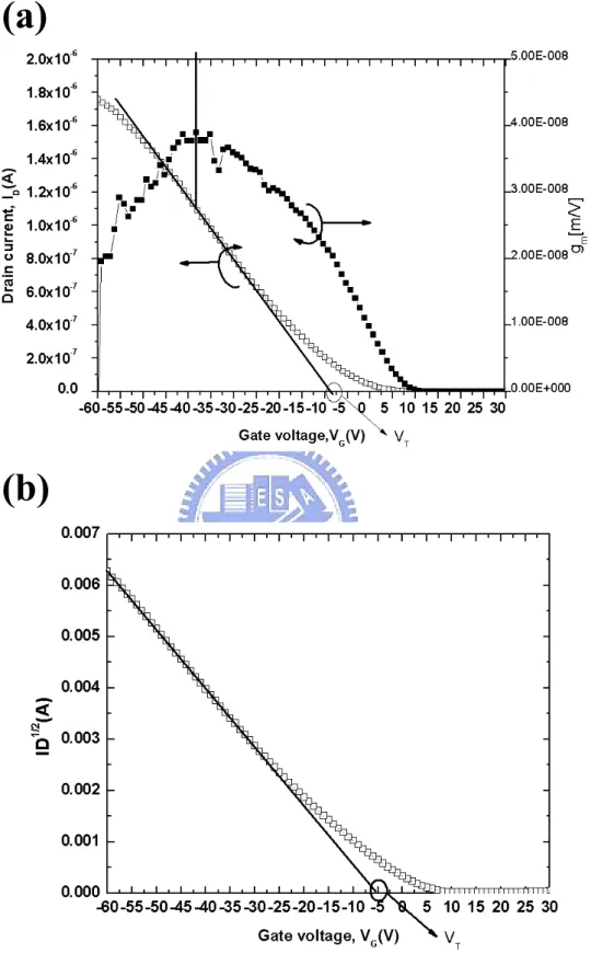
For threshold voltage, the way to obtain VTH is that a MOSFET with source terminal connected to ground, the drain current is measured with various gate biases. Drain terminal is applied a small value to make sure it operate in linear region. The expression of drain current is written as below:
(2-4)
For small drain bias the above expression is:- 20 -
(2-5)
Where W is channel width, L is channel length, Cox is capacitor per unit area. The equation (2-5) predicted that at a constant drain voltage by plotting ID-VG, a straighten line must be obtained. The inflexion point of the ID-VG plot is the point where the transconductance reaches its maximum. The threshold voltage is found at the intercept of tangent in the inflexion point with the VG axis [2.13]. The result of the VTH extraction method is shown inFig. 2-13 (a) for device operating in the linear region. When the device operates in the
saturation, the method to extraction the VTH is not the same. The drain current is measured at different values of VG, and at drain voltages that ensure the operation of the transistor in the saturation region: VD ≧max (VG) or VDG >0. The drain current obeys the same square law in saturation region.
(2-4)
In Fig.2-13 (b) is represented the extraction way to obtain VTH, resulting in a straighten line that intercepts the VG axis in VTH.
By plotting threshold voltage versus weight percentage, which is presented in the figure
2-14, P3HT FETs with 0.01wt%, 0.05wt%, 0.1wt%, 0.3wt%, and 1wt%, the value of VTH is
smaller than 2wt% sample. The threshold voltage of in lower 1 weight percentage sample is low. A large VTH, 496V, is obtained in 2wt% sample. Due to P3HT FETs in chloroform are normally on device, and it is hard to turn off. So applied a large bias at gate is to turn it off. General speaking, it does not to do so. As device scaling, small device has a trend in the future. If a large bias were applied, it would cause damage on device. Observing and zooming in 0.1 and 0.3 weight percentages, summarized in Table 2-4, the value of VTH is approaching zero. For device scaling, expect for the device dimension of 600/50(μm) with 0.1wt% in both xylene and chloroform, the rest of them are approached zero for threshold voltage.
2.5 Regioregularity and molecular weight
Both regioregularity and molecular can affect P3HT FETs performance. For those effects, there are many reports to investigate that without keeping the same datum, for example, the
- 21 -
obtained molecular weight are made and dissolved in different solvents. In this section, the material of P3HT will be dissolved in the same solvent, which is chloroform. In the beginning, the material of rr-P3HT (MW=55K, RR=90~93%) were purchased from FEM Inc, and Aldrich Chemical Company (MW=17K, RR>98.5%). All data were claimed by own companies. Although the material brought from different companies, a technology in making this material, like purity, is the same. Before go further, according to the results of the section 2.4.2, experimental terms and fabricated process flow are the same as below: weight percentage is fixed at 0.1wt%, and P3HT solute was dissolved in chloroform solvent.
Regioregularity value is based on purification method (refer to section 2.2), and MW is described below: the molecular formula is shown in Fig. 2-15. The molecular weight can be calculated based on its individual atoms number, and then summed all of them. The molecular formula of P3HT is (C10H18S)n, n is repeat unit of molecular, and their individual atom number are C=12, H=1, S=32. Total number in the brace is 170. n=100 (MW=17K) and n=323.5 (5~60K) are derived from molecular weight, for instant, MW=17K, there are hundreds monomer to compose of a long chain. The difference is known, and electrical result will be a goal.
In Fig. 2-15, all performance of high weight percentages is better than low one, even in off current. This result is suspect that a fixed a chain length, 50nm, high molecular could reach that easily, due to much repeat unit can perform the self-organization with less grain boundaries. For low molecular weight, first, it needs more three times of repeat unit to get the same result, compared to high molecule, and if low molecular weight would reach 50nm length, it would need more and more nanorods to gather around. Additionally, more of grain boundaries would be involved in the film. The rest of electrical parameters are summarized in the Table 2-5. The result in high molecular weight is higher one order of magnitude than low ones. It is possible to anticipate output characteristics in high molecular is better, and exhibit a good performance in both the linear and saturation regions, which is shown in the figure 2-16. From observed electrical result in my study, molecular weight is more important than the regioregularity.
- 22 -
2.6 Effect of various curing temperature
2.6.1 Fabrication process
All process procedure is the same as section 2.3. There is only one difference point, which is curing temperature. Curing temperature is varying in a range, 50℃, 100℃, 150℃, 200℃, and then set the device on hot plate for fixed 3 minutes. P3HTs were purchased from FEM Inc. (MW=55K, RR=90~93%).
2.6.2 Results and discuss
A set of transistors was fabricated with different curing temperatures. Over all of transistor were measured and plotted in Fig.2-3. Although the P3HT deposition conditions varied across these samples, the fabricated procedure is all the same.
The worse situation happed in both xylene and chloroform solvents at temperature 50 , which showed a large off current in Fig. 2-17(a), and leaded to a small value of on-off ratio. As you seen in Fig. 2-17(b), it shows typical On-Off ratios values versus the temperature with vary dimension devices. At temperature 50 degree, most low value of off current obtained in our study is around 102. Even in a situation of 100℃, compared with 150℃. Two possible reasons are suspected that first, at low temperature, 50℃; it is not enough to let the remnant solvents remove, the impurity drive off, which occupied the volume. In Fig. 2-18, a three-dimension analysis of surface morphology scanned by AFM can observe a hill-like surface, which could involve defects. When P3HT solution becomes a solid film, it involved many factors remind upper. Those factors lead to a low level of on-off ratio.
Electron Spectroscopy for Chemical analysis, ESCA, illustrated that the counts of oxygen in chloroform at 50℃ has second high level count in Fig. 2-19. The oxygen (1s) concentration is obtained during process producers, such as mixing with solvent and solute,
- 23 -
spin, and even it exists in atmosphere. The rest of elemental, sulfur and carbon, are the same, besides the case of xylene solvent. Sulfur (2p) and carbon (1s) cannot be detected in this analysis at this temperature fully. We doubt that the sulfur and carbon are less in the bulk of P3HT organic semiconductor, and this could be a reason for low mobility. Utilizing xylene to be a solvent is not appropriate.
Brian et al. [2.14] reported that annealing at 40-60 degree the concentration of oxygen is reduced, intermediate value of oxygen concentration is obtained at temperature of 80 ℃, and the concentration reached its lowest level when temperature is adding over 100 degree. This illustrated that anneal at low temperature the impurity will embed in the films, and could not been dedoped out off so that a production is formed within the pi-pi* gap. It will trap and de-trap the transport carriers.
Second, it is about physical property of polymer itself. During curing process, the temperature set at 50 degree, for P3HT polymer, it is near or under the glass transition temperature so that it is too low to provide energy. In general, the temperature could provide thermal energy, from heat source became kinetic energy, and causes a change in polymer such as intermolecular forces (bonding force are stronger between molecular and molecular, it needs to provide a thermal energy for polymer motion, which related to well-order, and enhance crosslink or interaction molecular each other), free volume of polymer (impurity or remnant solvents occupied the free volume, and the space of motion in polymer reduced)
[2.15] [2.16] [2.17].
Moreover, the molecular of polymer are not to have any segmental motion and dimensional change. A temporary distortion in covalent bond is occurred only. As you seen, the off current reduces with the temperature increasing, and these changes make on-off ratio increase between 100~150 degree. Summarized reasons are remnant solvent removeral, impurities dedope, polymer gained thermal energy to re-order, and free volume reduced and
- 24 -
then polymer could fit.
As curing temperature over 150 degree, both of field-effect mobility and on-off ratio decade dramatically, as shown in Fig.2-20. Curing at this temperature will be a challenge for P3HT organic polymer, due to organic is sensitive for temperature. Surface morphology is changing to more flatter. It indicates that remnant solvent will be removed and dedoped the impurity so that the volume has been changed. Also, at such temperature, pinhole could be formed, due to remnant solvent was dry out so fast, meanwhile P3HT solutions formed a solid film, and the voids could not be filled in time. For hopping carrier, pinhole treats as a barrier height in the channel.
The rigidity-flexible and conformation of organic polymer could be affected by temperature. P3HT has low energy barrier to rotation, molecular can rotated easily, which results high the flexibility of molecular. This rotation occurred at carbon single bond in main-chain structure with side-chain structure. It could not happen at heterocyclic of polythiophene. The reason is that the carbon double bond and polythophene had strongly bond energy. To break these double bonds needs higher bond dissociation energy. When P3HT molecule rotates with side-chain structure, the conformation will change to eclipsed conformation. Side structure is alkyl group; each side-alkyl aggressive or too close, the excluded force of van der Waals force (steric hindrance) could be form, as shown in Fig. 2-21, resulting low conjugality, stability, and low coplanarity. Low conjugality reduced the length of main chain, and affected the hopping carrier in the channel. This result is the same as section 2.4.3. There is an analogy with Brain et al.
For P3HT FETs in xylene, it is hard to measure the characteristics in 26400/50 dimension. In fact, using xylene to be a solvent seems not an appropriated choice. There are 8 transistors at each dimension, and most of them cannot be measured. This is reason for a few current yields.
- 25 -
2.7 Effect of various curing time
2.7.1 Fabrication process
Basically, all the process procedure is the same as section 2.3. There is only one difference, which is curing time. After the P3HT solutions in both xylene and chloroform spun onto SiO2, the device will be cured in 3 and 15 minutes, respectively. To see how curing time difference to affect electrical parameter.
2.7.2 Result and discuss
Figure 2-22 shows a transfer characteristic of P3HT FETs spin-coated from different
curing time. Both P3HT FETs in xylene and in chloroform exhibit that the performance of fixed at 3 minutes are better than 15 minutes, which is one order of magnitudes in on current. About the off current, it just exhibits a little change. The window of off current shows a vibration across those samples in our experiment.
According to the results, the suspect reason is that for long-duration curing time at 15 min, it could provide thermal energy from substrate for elemental oxygen, which would diffuse into the interface between organic active layer and silicon di-oxide. It embedded in the conducting channel and reduced the performance. This suspect could be supported by Auger depth analysis system in the Fig.2-23. Although the density of carbon and oxygen are much in the environment, measured data is very clear. Initially, the material of P3HT film exist four atomics, including carbon, oxygen, silicon, and sulfur (an atomic of hydrogen cannot be detected due to auger electron spectroscopy can detect atomic number lower 3). The atomic percentage in the bulk and conducting channel are rising, especially in 15min sample. Further, the concentration of oxygen for curing 3 minutes is higher than that of 15 minutes. It can be