氮化矽快閃記憶體可靠性量測與分析
64
0
0
全文
(2) 氮化矽快閃記憶元件可靠性量測與分析 SONOS Flash EEPROM Reliability Physics and Characterization. 研 究 生 : 馬煥淇. Student : Huan-Chi Ma. 指導教授 : 汪大暉 博士. Advisor : Dr. Tahui Wang. 國立交通大學 電子工程學系 電子研究所碩士班 碩士論文. A Thesis Submitted to Institute Electronics College of Electrical Engineering and Computer Science National Chiao Tung University in Partial Fulfillment of the Requirements for the Degree of Master of Science in Electronic Engineering June 2005 Hsinchu, Taiwan, Republic of China.. 中華民國 九十四 年 六 月.
(3) 氮化矽快閃記憶元件可靠性量測與分析. 學生:馬煥淇 國立交通大學. 指導教授:汪大暉 博士 電子工程學系. 電子研究所. 摘要. 本篇論文主要著重於特殊類型 SONOS 快閃式記憶元件之可靠性議題。其中包 括重複寫入/抹除之耐久性、寫入狀態之資料保存、抹除狀態之臨界電壓漂移、 讀取時之元件擾動。關於可靠性議題方面,抹除狀態資料遺失被觀測到。首先, 在一經過多次寫入抹除元件中,抹除狀態之臨界電壓會隨著儲存時間而漂移。此 漂移與溫度呈現弱相關。臨界電壓漂移與時間的相依性,可用穿隧波前模型來做 完整的描述。此外,在兩位元操作下,有著明顯的讀取擾動效應。而一正電性之 氧化層電荷導致通道電子注入之解析模型,被用來闡明此讀取擾動特性。氮化矽 層電荷透過氧化層缺陷導致穿隧而造成之資料遺失,在此也被描述。Frenkel-Poole 散失為此最主要的機制。 另外,我們觀測到短時間因寫入動作干擾所引發的可靠性議題,並研究因隨 機雜訊所引發之讀取電流不穩定,此一不穩定現象會隨著寫入/抹除次數增加和閘 極長度微縮而變差。且利用通道熱電子所寫入之不均勻電荷分佈亦會擴大其效 應。憑藉在本篇論文中所提及之氧化層改進方法,此種負面現象將得以舒緩。. i.
(4) SONOS Flash EEPROM Reliability Physics and Characterization. Student: Huan-Chi Ma. Advisor: Dr. Tahui Wang. Department of Electronics Engineering & Institute of Electronics National Chiao Tung University. Abstract. The reliability issues of two-bit storage nitride flash memory cells including low-Vt state threshold voltage instability, read-disturb, and high-Vt state charge loss will be addressed. Program-state retention loss due to nitride charge escape via oxide trap assisted tunneling is also characterized. Frenkel-Poole emission is found to be the dominant mechanism. In addition, erase-state data loss is explored. An erase-state threshold drift with storage time is observed in a P/E cycled cell. This drift has insignificant temperature dependence. The temporal evolution of the threshold voltage drift can be well described by the tunneling front model. Furthermore, significant read-disturb effect is noticed in two-bit operation. An analytical model based on positive oxide charge assisted channel hot electron injection has been developed to explain the read-disturb behavior. Our study shows that the cell reliability. ii.
(5) is strongly dependent on operation methods and process conditions. Furthermore, program/erase cycling induced random telegraph noise in read current noise is observed. The amplitude of current fluctuation increases with P/E cycle number and with decreasing gate length. Non-uniform charge storage by CHE programming can further enhance read current fluctuation. The improvement of bottom oxide reliability can significantly reduce this effect.. iii.
(6) Contents Chinese Abstract English Abstract Acknowledgements Contents Figure Captions Chapter 1 Introduction Chapter 2 High-Vt State Charge Loss 2.1. Introduction. 2.2. Oxide Charge Detrapping Mechanism. 2.3. Nitride Charge Retention Loss 2.3.1 Movement of Trapped Nitride Charge 2.3.2 Data Retention Model. Chapter 3. Low-Vt State Reliability Issues. 3.1. Introduction. 3.2. Room-Temperature threshold Voltage Drift 3.2.1 Mechanisms for Vt Drift 3.2.2. 3.3. Time Dependence of Vt Drift. Read-Disturb Effects in Erase State 3.3.1. Cause of Read-Disturb Effects in Erase State. 3.3.2. Commonality between Vt Drift and Read-Disturb. 3.3.3. Read-Disturb Behavior. 3.3.4 PCAT Model in Read-Disturb 3.4. Over-erase. v. i ii iiv v vii 1 5 5 5 7 7 16 22 22 22 22 27 29 29 29. 29 29 35.
(7) Chapter 4. P/E Cycling Induced Read Current Noise. 4.1. Introduction. 4.2. Random Telegraph Noise Measurement. 4.3. P/E Cycling Stress. 4.4. Length Dependence & Non-uniform Vt Effect. 4.5. Oxide Process Effect. Chapter 5. Conclusion. 37 37 37 38 38 45 48. Reference. 49. vi.
(8) Figure Captions Fig. 1.1. Schematic representation of a SONOS cell and two-bit storage. The shaded area in the nitride layer represents stored charges.. Table 1.1 Suggested bias conditions for MXVAND cell operation. Fig. 2.1. Program-state retention loss versus P/E cycles.. Fig. 2.2. Threshold voltage plotted against drain bias in a fresh device. T=25oC and 85oC.. Fig. 2.3. Threshold voltage versus drain bias in a 100k P/E cell.. Fig. 2.4. Dependence of threshold voltage on retention time in a fresh cell. Gate bias is 0V,-3V and -6V in retention measurement state.. Fig. 2.5. Dependence of threshold voltage on retention time in a 100k P/E device. Retention gate bias is 0V,-3V and -6V.. Fig. 2.6. Dependence of GIDL/GISL and threshold voltage on retention time in a fresh device.. Fig. 2.7. Dependence of GIDL/GISL and threshold voltage on retention in 100k P/E device.. Fig. 2.8. Program-state charge loss characteristics in a fresh and a 100k P/E NROM cells. T=25oC and 85oC.. Fig. 2.9. Illustration of stored charge loss by Frenkel-Poole emission and subsequently oxide trap assisted tunneling.. Fig. 2.10 Measured nitride charge detrapping current in a large area device at Vg=-6V. The device was subject to FN stress at Vg=-20V for 2000s. Fig. 2.11 High-Vt state charge loss versus applied gate bias (top axis). The bottom axis corresponds to the square root of the nitride electric field. Vo is the flat-band voltage in high-Vt state. Fig. 3.1 Typical Vt retention characteristics in a fresh and a 100k P/E cycled cell.. vii.
(9) Fig. 3.2(a) Measurement setup of positive oxide charge detrapping induced substrate current (Ib). Fig. 3.2(b) Pre-stress and post-stress substrate currents in two large area devices (500µm×500µm). FN stress was at Vg= -18V for 3000s. Substrate current was measured at Vg=VFB. Fig. 3.3. Room temperature Vt drift in two 10k P/E cycled NROM cells fabricated with different ONO process. The cell size is Lg =0.5µm and Wg =0.35µm.. Fig. 3.4. Schematic band diagram showing positive oxide charge and negative nitride charge in a 1k P/E cycled device. The electrons in valence band and conduction band can tunnel to recombine with positive oxide charge via path A and path B.. Fig. 3.5. Dependence of Vt shift on read-disturb time in a 1k P/E cycled cell. Power-law time dependence (tn) is obtained. The read bias condition is Vg=3V, Vd=2.5V.. Fig. 3.6. Illustration of positive charge assisted electron tunneling current (Isd) in gate disturb.. Fig. 3.7. Hot carrier read-disturb caused Vt in a fresh cell and in a 10k P/E cycled cell. The disturb time is 104s.. Fig. 3.8. Temperature effect on read disturb of 1k P/E cycled cells. Devices with a gate length of 0.5µm, 0.4µm and 0.3µm are characterized. The applied gate and drain biases are 3V and 1.6V, respectively, and the disturb time is 104 sec.. Fig. 3.9. The evolution of erase-state Vt with storage time in an over-erased cell. The band-to-band hot hole injection.. Fig. 4.1. Experimental setup for RTN measurement.. Fig. 4.2. Representative RTN traces in a NROM cell (W/L=0.35µm/0.3µm). (a) fresh, (b) 1k P/E cycles, (c) 100k P/E cycles.. Fig. 4.3. Comparison of RTN amplitude in program-state and in erase-state (b) Dependence of ∆Id (two-level transition) on read current. The P/E cycle number is 100 P/E. The reverse read bias is Vg=4V, Vs=1.5V and Vd=0V.. viii.
(10) Fig. 4.4. (a) Comparison of RTN amplitude for Lg=0.3µm and 0.5mm. (b) Dependence of ∆Id (two-level transition) on gate length. The read current level is about 1µA.. Fig. 4.5. Calculated gate length dependence of two-level RTN amplitude from 2D device simulation. For CHE injection, the trapped charge width is assumed to be 30nm. FN injection has uniform charge storage. The parameters in simulation are not calibrated.. Fig. 4.6. Typical RTN traces for uniform FN injection (a) and channel hot electron injection (b). Both cells have the same P/E stress conditions.. Fig. 4.7. Maximum ∆Id observed at a read current of 30µA from multi-level RTN. The sampling size is 105 readings.. Fig. 4.8. (a) The increment of charge pumping current (Icp) in device A and device B after 10k P/E cycles. (b) RTN traces in Device A after 10k P/E cycles (c) RTN traces in Device B after 10k P/E cycles.. ix.
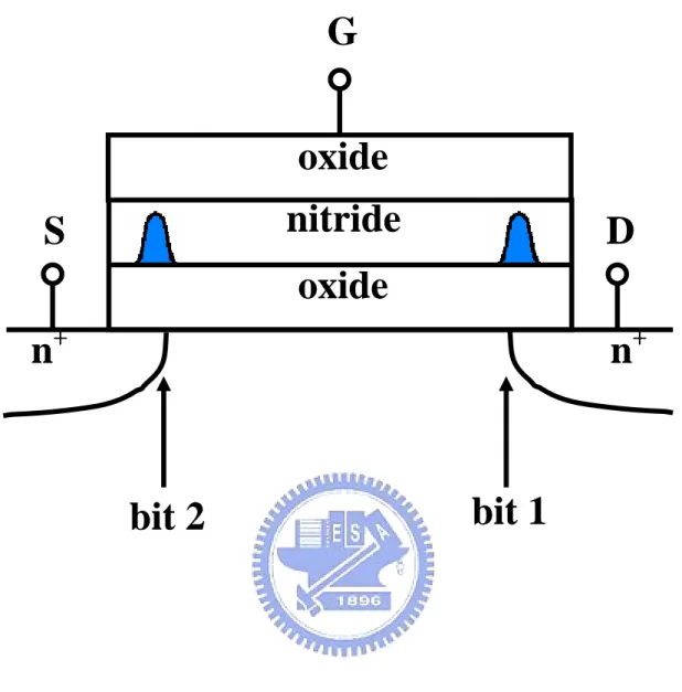
(11) Chapter 1 Introduction Currently, two major research thrusts in nonvolatile semiconductor memory are underway. One has data stored in a multi-layer gate structure in a field effect transistor and the other takes advantage of electrical polarization of ferroelectric material in a ferroelectric capacitor/transistor [1]. With respect to charge storage devices, there are two kinds of them. (a) Charge Trapping Devices: Charge is stored in traps at the interface of a multi-layer gate structure and/or in the bulk of insulator, such as the metal nitride oxide silicon (MNOS) structure [2], [3]. (b) Floating Gate Devices: Charge is stored in a thin conducting or semiconductor layer or conducting particles sandwiched between insulators [4], [5]. However, since its invention in 1967, the nitride-based nonvolatile memory structures, both MNOS and polysilicon oxide-nitride-oxide silicon (SONOS) [6]-[10], have received limited commercial acceptance due to their employment of ultra-thin dielectric (~20Å) and their non-ideal charge retention characteristics. In conventional SONOS cells, charges are stored uniformly in the nitride layer. This SONOS concept has recently evolved into a two-bit storage cell (NROM). Recently, the new SONOS flash EEPROM cell has soon gained great attention for their smaller size per bit (2.5F²/bit in Flash, where F is the feature size of the process) [11], [12], less fabrication complexity [13], no drain turn-on and better charge retentivity [14] This SONOS cell is made of a n-channel MOSFET with an oxide-nitride-oxide gate dielectric structure, as shown in Fig.1.1. The major difference between NROM and the conventional SONOS devices [15] is that the bottom oxide is about 60Å [11], which is much thicker than that of SONOS (~20 Å), where direct tunneling is involved for charge transport.. By taking advantage of localized charge storage in the nitride layer above the n+. 1.
(12) source and drain junctions, two-bit per cell operation can be achieved. Channel hot electron injection and band-to-band hot hole injection are utilized for programming and erasing, respectively. Table.1.1 shows the operation bias of program, erase, and read [16]. In this thesis, the reliability issues of the nitride flash cells will be reviewed. Responsible mechanisms and possible solutions will be discussed. Following the introduction, high-Vt state charge loss will be discussed in chapter two. In chapter three, we will discuss low-Vt state reliability issues. We will demonstrate a micro-second transient measurement circuit to investigate program disturb effect. Random telegraph noise induced read current fluctuation will be discussed in chapter four. Finally, we will make a conclusion of this thesis.. 2.
(13) G oxide nitride. S. D. oxide n+. n+. bit 1. bit 2. Fig. 1.1. Schematic representation of a SONOS cell and two-bit storage. The shaded area in the nitride layer represents stored charges.. 3.
(14) Table.1.1. Bit 1. Bit 2. Suggested bias conditions for MXVAND cell operation.. Program. Erase. Read. Vg. 11V. -3V. 2.5V. Vd. 5V. 8V. 0V. Vs. 0V. 0V. >1.5V. Vg. 11V. -3V. 2.5V. Vd. 0V. 0V. >1.5V. Vs. 5V. 8V. 0V. 4.
(15) Chapter 2 High-Vt State Charge Loss 2.1 Introduction One of the major advantages of the NROM cell, as compared with the floating gate flash EEPROM, is the better retentivity due to localized charge trapping [17]. The retention loss characteristics of the NROM are determined by two factors. (i) oxide charge detrapping (Qox) [18], and (ii) nitride charge loss (QSiN) [19]. The amount of created oxide trapped charge is dependent on P/E stress and oxide quality. In this cell, due to a thick bottom oxide, nitride charge escape to the substrate has to go through a two-step process, i.e. electron emission from nitride traps to the nitride conduction band and subsequently escape to the substrate via oxide trap assisted tunneling. Thus, nitride charge loss is also dependent on trap creation in the bottom oxide. Fig. 2.1 shows the retention loss versus P/E number. At low P/E stress, oxide trap creation is minimal and thus charge retention loss is small.. 2.2 Oxide Charge Detrapping Mechanism With respect to oxide charge detrapping, we utilize the so-called tunneling front model [20] to describe the charge detrapping behavior. A tunneling front moving through the oxide with distance/time dependence is given by. xm (t ) = (2 β ) −1 ⋅ ln(t t 0 ). (2.1). where xm(t) is the position of the front as a function of time t, β is the tunneling constant, and t0 is the characteristic tunneling time. Because of the sharpness of the moving tunneling front, the charge passed by the front can. 5.
(16) be considered to be totally detrapped. The amount of charge escaping, ∆Q(t), via tunneling at time t can be approximated by. ∆Q(t ) = q ∫. xm ( t ). 0. dx ⋅ N ( x). (2.2). where x is the distance from the Si-SiO2 interface, q is the electronic charge, and N(x) is the spatial distribution of charged oxide traps. Note that for a uniform trap distribution Nox, a logarithmic time dependence of ∆Q can be derived immediately from Eqs.(2.1) and (2.2), as shown in Eq.(2.3). ∆Q(t ) =. qN ox t ln( ) 2β t0. (2.3). According to the simple quantum mechanical two-band, one-electron tunneling theory, we can derive the tunneling parameter β as. ⎡ 2m * ⎤ β = ⎢ 2 Eto ⎥ ⎣ h ⎦. 12. (2.4). where m* is the tunneling effective mass of the trapped charge in oxide and Eto is the oxide trap energy. Finally, the threshold voltage shift due to oxide charge escape is. ∆Vth = −2.3. t ONO. qhN OX. ε ONO 2 2m Eto *. 6. log. t t0. (2.5).
(17) where tONO and ε ONO are the equivalent thickness and dielectric constant of the ONO dielectrics, respectively.. 2.3 Nitride Charge Retention Loss. 2.3.1 Movement of Trapped Nitride Charge The retention loss occurs either due to charge escape in the vertical direction (vertical retention loss [21]) or due to lateral redistribution of the trapped charge within nitride (lateral retention). Recently, Eitan’s group makes efforts to investigate the cause of the charge loss in a NROM-like cell [11]. They claimed that the root cause of the threshold voltage lowering is lateral spread of stored charges since vertical retention is guaranteed by adopting a thick bottom oxide to avoid charge direct tunneling. Their argument is definitely correct in a fresh cell. However, it’s not straightforward in a cycled cell due to the presence of oxide trap assisted tunneling. The lateral distribution of the trapped nitride charge can be deduced at least qualitatively by the dispersion of the threshold voltage versus drain bias. As drain bias increases, the junction depletion region extends further into the channel. The nitride charge above the depletion region is “masked” and does not affect the threshold voltage. Fig. 2.2 shows the measured threshold voltage versus drain bias in a fresh device. To enhance charge movement in the nitride layer, the sample was baked at 85C for 1900 sec. The Vt-Vd after the bake is shown in the figure for a comparison. No significant change is noticed. The result in Fig. 2.2 suggests that lateral movement of the nitride charge is insignificant. We also measured the Vt-Vd in a 100k P/E device (Fig. 2.3). Similarly, lateral movement of the nitride charge is not observed. However, we observe a slight threshold voltage reduction at 85C bake, an evidence of charge loss in the vertical direction. Interestingly, if we applied a negative gate bias of 3V. 7.
(18) during bake, a significant threshold voltage decrease is found in Fig. 2.3. From the above findings, we believe that the data retention loss is caused by charge escape in the vertical direction, since the application of a vertical field (Vg=-3V) apparently has a large influence on charge retention capability. Next, we would like to investigate the influence of vertical field on charge retention loss in program state. Three different gate biases are applied in the retention measurements. Fig.2.4 shows the threshold voltage evolution with retention time in a fresh cell. No charge loss is observed for all three gate biases. The reason is that the bottom oxide in the fresh device is clean. As pointed out earlier, nitride charge loss is improbable without oxide trap assisted tunneling. At low P/E cycles, the bottom oxide plays a blocking role for nitride charge loss. In the 100k P/E device, apparent gate bias dependence of charge retention loss is obtained in Fig.2.5. As a conclusion, vertical retention loss is a dominant mechanism in a P/E cycled cell, which exhibits strong vertical field dependence. The following measurement provides another evidence to exclude the possibility of lateral movement in the retention loss. Here, we use uniform channel FN injection rather than hot electron injection for programming. In this way, the injected nitride charge has a uniform distribution. The possibility of lateral movement can be ruled out completely in this case. Then, we use GIDL and GISL [22] to monitor the variation of charge in the two ends of the channel during retention measurement. Fig. 2.6 shows the measured result in a fresh cell. The GIDL/GISL are constant in the entire measurement period. In a P/E stressed device ( stressed at the drain side), the threshold voltage and GISL still keep unchanged during the measurement, but GIDL decreases with time, as shown in Fig.2.7. The threshold voltage does not change because only the drain side is damaged and charge loss takes place in the drain side. The potential barrier in the channel region is mostly unaffected. Similarly, GISL does. 8.
(19) Retention loss(Volts). 0.8 0.6 0.4 0.2 0.0. 3. 10. 4. 5. 10. 10. P/E cycles. Fig. 2.1. Program-state retention loss versus P/E cycles.. 9. 6. 10.
(20) Threshold voltage(Volts). 4.5 4.0 3.5 3.0 2.5 2.0 1.5 1.0 0.5 0.0 0.0. o. 25 C o 85 C,bake 2000sec. 0.2 0.4 0.6 0.8 1.0. 1.2. 1.4. Drain bias(Volts). Fig. 2.2. Threshold voltage plotted against drain bias in a fresh device. T=25oC and 85oC.. 10.
(21) Threshold voltage(Volts). 4.5 4.0 3.5 3.0 2.5 2.0 1.5 1.0 0.5 0.0 0.0. o. 25 C o 85 C,bake 2000sec. o Vg=-3V,85 C bake 2000sec. 0.2. 0.4. 0.6. 0.8. 1.0. 1.2. Drain bias(Volts). Fig.2.3. Threshold voltage versus drain bias in a 100k P/E cell.. 11. 1.4.
(22) Threshold voltage(Volts) Fig. 2.4. 5.0 4.5 4.0 3.5 3.0 2.5 2.0 1.5 1.0 0.5 0.0 -1 10. Vg=0V Vg=-3V Vg=-6V 0. 10. 1. 10. 2. 10. 3. 10. Retention time(sec.). Dependence of threshold voltage on retention time in a fresh cell. Gate bias is 0V, -3V and -6V in retention measurement state.. 12. 4. 10.
(23) Threshold voltage(Volts) Fig. 2.5. 5.0 4.5 4.0 3.5 3.0 2.5 2.0 1.5 1.0 0.5 0.0 -1 10. Vg=0V Vg=-3V Vg=-6V 0. 10. 1. 10. 2. 10. 3. 10. Retention time(sec.). Dependence of threshold voltage on retention time in a 100k P/E device. Retention gate bias is 0V, -3V and -6V.. 13. 4. 10.
(24) GIDL(nA) vs. GISL(nA). 4 3 1. 2. 0.1. 0. GIDL GISL 100 200. 1 300. 400. 500. Retention time(sec.). Fig. 2.6. Dependence of GIDL/GISL and threshold voltage on retention time in a fresh device.. 14. 0. Threshold voltage(Volts). 5. 10.
(25) GIDL(nA) vs. GISL(nA). 4 3 1. 2. 0.1. 0. GIDL GISL 100 200. 1 300. 400. 500. Retention time(sec.). Fig. 2.7. Dependence of GIDL/GISL and threshold voltage on retention time in a 100k P/E device.. 15. 0. Threshold voltage(Volts). 5. 10.
(26) not change with time since GISL is affected only by the charge at the source end. This distinctly different feature of GISL and GIDL in Fig. 2.7 implies that the retention loss is correlated with oxide defects created by P/E stress. In summary, there are two factors affecting the nitride charge loss; (1) temperature, and (2) the damage due to cycling stress. Temperature will accelerate trapped charge emission rate but on the other side may cause oxide trap annealing and reduce the retention loss [23].. 2.3.2 Data Retention Model In this section, we will focus on the modeling of nitride charge detrapping processes in a NROM device. In our discussion, it’s assumed that blocking oxide is thick enough to prevent any charge loss. All four device terminals are grounded when devices are in the retention mode. The nitride film is initially filled with injected electrons. Fig.2.8 shows the retention characteristics at different P/E cycles. The cycling number and temperature dependence in Fig.2.8 implies that the stored nitride charge loss is through thermionic-field emission (Frenkel-Poole model [24]) and subsequently oxide trap assisted tunneling [25]. These processes are illustrated in Fig.2.9. The nitride charge emission time can be written below,. τ N = τ 0 exp((φ N − q(qE / πε )1 2 ) / kT ). (2.6). where φN is the nitride trap energy, E is the electric field in nitride and other variables have their usual definition. The nitride charge emission current and the corresponding Vt shift can be derived as follows,. 16.
(27) Threshold voltage(Volts). 5.5 5.0. fresh. 4.5. 100K. 4.0. 100K. 3.5 o. 3.0 2.5. Fig. 2.8. T=25 C o T=85 C 1. 10. 2. 3. 4. 10 10 10 retention time(sec.). Program-state charge loss characteristics in a fresh and a 100k P/E NROM cells. T=25℃ and 85℃.. 17.
(28) EC F.P. Nox. •. nitride. Si-substrat oxide Fig. 2.9. Illustration of stored charge loss by Frenkel -Pooleemission and subsequently oxide trap assisted tunneling.. 18.
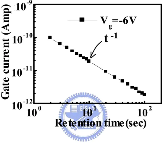
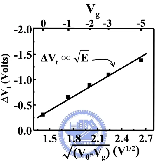
(29) IN=AQN. ∆Vt (t)=. dφN AQNkT = t dt. QN CONO. [q(. (2.7). qE 1/2 t )] ) + kT ln( τ0 πε. (2.8). where QN represents trapped charges in nitride per unit area and per unit trap energy. In the above derivation, we make the following assumptions. First, we assume that at measurement time t all nitride traps with time constants less than t are completely emptied and all other traps are unaffected. Secondly, we assume that nitride trapped charge escape is limited by the FP emission, i.e., trap-assisted tunneling in bottom oxide much faster than the FP emission. This assumption is reasonable in a heavily P/E cycled cell where bottom oxide stress is severe. Third, we assume that emitted nitride charges in a measurement interval from 1 second to 100 seconds (Fig. 2.10) have a uniform distribution in trap energy, i .e. , QN a constant . This assumption is also reasonable since the trap energy span in the measurement period is only about kTln(100)~0.12eV. For a constant energy distribution of nitride trapped charges, the nitride charge emission current obeys a 1/t relationship (Eq.(2.7) & Fig. 2.10) and the Vt loss is proportional to the square root of the electric field (Eq.(2.8) & Fig. 2.11).. 19.
(30) Gate current (Amp). 1x10. -9. V g=-6V. 1x10. -10. 10. -11. 10. -12. Fig. 2.10. t -1. 10. 0. 10. 1. 10. 2. Retention time(sec). Measured nitride charge detrapping current (IN) in a large area device at Vg=-6V. The device was subject to FN stress at Vg= -20V for 2000s. 20.
(31) ∆Vt (Volts). -2.0. 0. -1. Vg. -2 -3. -5. -1.5 ∆V ∝ E t -1.0 -0.5 0.0. Fig. 2.11. 1.5 1.8 2.1 2.4 2.7 1/2) ( V (V0-Vg) High-Vt state charge loss versus applied gate bias (top axis). The bottom axis corresponds to the square root of the nitride electric field. Vo is the flat-band voltage in high-Vt state.. 21.
(32) Chapter 3 Low-Vt State Reliability Issues 3.1 Introduction In this chapter, we will discuss three erase-state retention loss phenomena, room temperature (RT) threshold voltage drift, read-disturb and over erase. The responsible physical mechanisms will be investigated.. 3.2 Room-Temperature Threshold Voltage Drift 3.2.1 Mechanism of Vt Drift The NROM cell exhibits excellent data retention behavior before P/E cycling. After P/E stress, a positive erase-state Vt drift with a logarithmic time-dependence is observed (Fig. 3.1). This Vt drift does not have temperature dependence. Positive oxide charge tunnel detrapping was proposed [28] to explain this phenomenon. In order to measure positive oxide charge detrapping current directly (Fig. 3.2(a)), large area devices were fabricated with two different ONO processes (A and B). Process B is known to have better oxide endurance. The substrate current (Ib) before and after FN stress was measured in these two samples. According to the hole tunneling front model [29], the post-stress substrate current resulting from positive oxide charge detrapping follows a 1/t time-dependence,. Ib(t)=A. Qox -1 αh t. (3.1). αh=4π 2mφox /h. (3.2). where Qox is the positive oxide charge density, φox denotes the energy barrier of positive. 22.
(33) trapped charges and A is the area of the device. Fig. 3.2(b) shows the measured pre-stress and post-stress substrate currents versus time. Note that process B exhibits a smaller post-stress substrate current because of less positive oxide charge creation. Fig. 3.3 shows the measured Vt drift in two 10k P/E cycled cells. By comparing the two ONO processes, a correlation between the Vt drift and Ib is obtained.. 23.
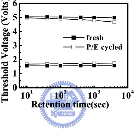
(34) Threshold Voltage (Volts) Fig. 3.1. 6 5 4. fresh P/E cycled. 3 2 1 0. 10. 1. 2. 3. 10 10 Retention time(sec). 10. 4. Typical Vt retention characteristics in a fresh and a 100k P/E cycled cell.. 24.
(35) Vg O N O. +. n+. Ib. n+. Substrate current (Amp). (a). 10. -11. t. 10. -12. 10. -13. 10. -14. Process A Process B. -1. post-stress pre-stress. 0. 1. 2. 10 10 10 Measurement time(sec) (b). Fig. 3.2(a). Measurement setup of positive oxide charge detrapping induced substrate current (Ib).. Fig. 3.2(b). Pre-stress and post-stress substrate currents in two large area devices (500μm × 500μm). FN stress was at Vg = -18V for 3000s. Substrate current was measured at Vg=VFB.. 25.
(36) Threshold Voltage (Volts) Fig.3.3. 2.0 1.9 1.8. Process A. 1.7 1.6 1.5. Process B 1. 2. 3. 10 10 10 10 Retention time(sec). 4. Room temperature Vt drift in two 10k P/E cycled NROM cells fabricated with different ONO process. The cell size is Lg =0.5µm and Wg = 0.35µm.. 26.
(37) 3.2.2 Time Dependence of Vt Drift To explain the observed time-dependence of the RT drift, the tunneling front model discussed in Chapter 2 is employed. In a P/E stressed device, the trapped hole in the bottom oxide can escape to the substrate via tunneling. Based on the tunneling front model, the threshold voltage shift caused by valence band electron tunneling is illustrated by path A in Fig.3.4. ∆Vth = −2.3. t ONO qhN ox log t ε ONO 2 2m * ( φ B + E g ). (3.3). and the threshold voltage shift caused by conduction band electron tunneling is illustrated by path B in Fig.3.4. ∆Vth = −2.3. t ONO qhN ox log t ε ONO 2 2 m * ( φ B ). 27. (3.4).
(38) φB B. QSiN. Fig.3.4. QOX. A. ec ev. Schematic band diagram showing positive oxide charge and negative nitride charge in a 1k P/E cycled device. The electrons in valance band and conduction band can tunnel to recombine with positive oxide charge via path A and path B.. 28.
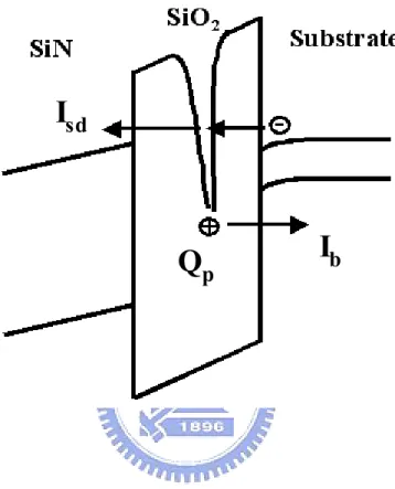
(39) 3.3 Read-Disturb Effects in Erase State 3.3.1 Cause of Read-Disturb Effect Read-disturb effect is twofold. The wordline voltage during read may enhance the RT drift in the neighboring bit. On the other side, the relatively large read bitline voltage may cause channel hot electron injection and result in a significant threshold voltage shift of the neighboring bit. The hot electron injection caused Vt shift follows power-law timedependence. An analytical model based on positive oxide charge assisted channel hot electron.. 3.3.2 Commonality between Vt Drift and Read-Disturb The RT drift and read-disturb have something in common. We performed RT drift measurement and the read-disturb measurement in the same device sequentially. No matter the RT drift or the read-disturb is measured first, the subsequent read-disturb or RT drift is significantly reduced. From the study in the preceding section, we believe that read-disturb is also related to trapped charge in the bottom oxide.. 3.3.3 Read-Disturb Behavior At Vg=3.0V, Vd=2.5V, the read-disturb caused Vt shift follows a power-law time dependence (tn) (Fig. 3.5). Channel electrons can gain sufficient energy from a large electric field to inject into the nitride conduction band and then get trapped in the nitride. In the next section, we will develop the read-disturb model based on the channel hot electron injection into the SiN via positive charge assisted tunneling (PCAT).. 3.3.4 PCAT Model in Read-Disturb. 29.
(40) The columbic potential of a positive oxide charge acts as a sequential tunneling center. The channel hot electron injection into nitride via PCAT is illustrated in Fig.3.6. Icat is positive charge assisted electron tunneling current.. I cat ∝ t − P , P = (. m e φe 1 2 ) m h φh. (3.6). The time dependence of the threshold voltage shift from Icat injection is derived in the following.. ∆Vth ∝ ∫ I cat ( t )dt = ∫ t − P dt = t 1− P = t n. (3.7). It is a general trend in literature to have m h ≥ m e [29-31] and φh ≥ φe [32,20]. Thus the power factor P in Eq.3.6 is expected to be smaller than 1 and the extracted value of P in [33] is about 0.7. In other words, n is about 0.3, which is consistent with our measured result. Moreover, since the bit-line voltage in reverse read must be sufficiently large to overcome the stored charge of the second bit, hot electron injection during read should be considered. The hot electron read disturb is worsened in a P/E cycled cell because of positive oxide charge enhanced electron injection. Fig. 3.7 shows the Vt shift versus read bit-line voltage in a fresh device and in a 10K P/E cycled NROM cell [34]. The read disturb increases drastically as the read voltage is above 2V. Lower operating temperature and shorter gate length will aggravate hot electron read disturb (Fig. 3.8). Various methods were proposed [35, 36] to reduce the positive oxide charge enhanced read-disturb.. 30.
(41) Threshold voltage shift(Volts) Fig.3.5. 1. 0.1. 3. 4. 10. 10. Read disturb time(sec.). Dependence of Vt shift on read-disturb time in a 1k P/E cycled cell. Power-law time dependence (tn) is obtained. The read bias condition is Vg=3V, Vd=2.5V.. 31.
(42) Isd. Qp. Fig.3.6. Ib. Illustration of positive charge assisted electron tunneling current (Isd) in gate disturb.. 32.
(43) ∆Vt (Volts). 1.0 0.8 0.6. fresh 10k P/E V g=3V. 0.4 0.2 0.0. 1.0. 1.5. 2.0. 2.5. Read Bitline Voltage(Volts) Fig.3.7. Hot carrier read-disturb caused ∆Vt in a fresh cell and in a 10k P/E cycled cell. The disturb time is 104s.. 33.
(44) 1.0 -20C 25C 85C. ∆Vt(V). 0.8 0.6 0.4 0.2 0.0 0.2. 0.3. 0.4. 0.5. 0.6. Channel length(μm) Fig.3.8. Temperature effect on read disturb of 1k P/E cycled cells. Devices with a gate length of 0.5µm, 0.4µm and 0.3µm are characterized. The applied gate and drain biases are 3V and 1.6V, respectively, and the disturb time is 104 sec.. 34.
(45) 3.4 Over-erase. One major reliability concern in a NROM cell comes from the lateral migration of trapped charges in the nitride layer [37]. This effect is more serious in hole accumulation state (erase state) since trapped holes are more mobile than electrons in a nitride [38]. To investigate hole lateral movement in erase state, an extremely strong band-to-band hot hole injection condition is used.. As opposed to the RT Vt drift, the over-erased cell shows a negative Vt drift with. time (Fig. 3.9). This effect is more significant at higher temperatures and is attributed to trapped hole hopping in the lateral direction [39].. 35.
(46) ∆Vt (Volts). 0.0 -0.1 -0.2 T=85C T=150C T=250C. -0.3 -0.4. 10. 3. 10. 4. 10. 5. Retention time(sec). Fig.3.9. The evolution of erase-state Vt with storage time in an over-erased cell. The band-to-band hot hole injection. 36.
(47) Chapter 4 P/E Cycling Induced Read Current Noise 4.1 Introduction In this chapter, we investigate P/E cycling induced random telegraph noise (RTN) in non-uniform charge storage nitride flash cells for the first time. The amplitude of RTN increases with P/E cycle number and with decreasing gate length. Non-uniform charge storage by channel hot electron programming can further enhance read current fluctuation. The large amplitude of read current fluctuation implies we must allow for more margins in cell operation and needs careful attention especially in Multi-level cell (MLC) application. Therefore, to probe the RTN phenomenon and to find the solutions will be an important issue in SONOS type two-bit storage flash memory cells. According to our investigation, read current noise can be significantly reduced by the improvement of bottom oxide reliability.. 4.2 Random Telegraph Noise Measurement The charge transport through a MOSFET device characterized by discrete switching events of the drain current, has often been observed and attributed to the trapping/detrapping of conduction carriers by a single defect near Si/SiO2 interface [37]-[39]. Different names exist for the phenomenon, like burst noise or Random Telegraph Noise (RTN). Micro-second Transient measurement system for measuring read current noise is shown in Fig. 4.1. This setup can monitor the drain current noise in fixed read bias. The sampling rate in our experiments is 10kHz, which enables the observation of fast transitions of read current with time constant down to 0.1ms, which corresponds to 105 reading in each measurement of 10 seconds. The devices used in this work have a gate length of 0.35µm and a gate with from 0.5µm to 0.3µm.. 37.
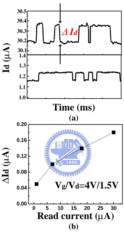
(48) 4.3 P/E Cycling Stress In a P/E cycled cell, the read current fluctuation induced by oxide trap is found to be larger than that in a fresh cell. Fig. 4.2 shows read current fluctuation at program state in a fresh cell, after 1k P/E cycles and after 100k P/E cycles. The cell biased in weak inversion and the read current is near 1µA. The apparent random telegraph noise patterns are observed in a 100k P/E cycled cell while it is undetected in a fresh cell. The RTN rises from the charging/discharging of single oxide trap or multiple oxide traps created by P/E cycling stress [40]. At a low cycle number the RTN exhibits two-level transitions (Fig. 4.2(b)) while at a large cycle number multi-level transitions (4-level) are occasionally observed (Fig. 4.2(c)). These multi-level transitions, superimposed by several independent two-level RTN waveforms, may exhibit a large ∆Id and result in a read failure. The dependence of noise amplitude on read current level is shown in Fig. 4.3. In this measurement, a NROM cell is programmed to different Vt and the reverse read bias is at |Vds|=1.5V and Vgs=4V. The cycle number is 100 that only two-level transitions are obtained. As shown in Fig. 4.3(a), ∆Id is found to increase from 0.04µA in a high-Vt cell (1µA read current) to 0.18µA in a low-Vt cell (30µA read current).. 4.4 Length Dependence & Non-uniform Vt Effect The gate length effect on RTN is shown in Fig. 4.4. The read current level is about 1µA. The RTN amplitude with two-level transitions is shown in Fig. 4.4(a), a noticeable increases of ∆Id with decreasing gate length [41]. A two-dimensional device simulation is performed to calculate the gate length dependence. A similar trend is obtained (Fig. 4.5). Moreover, RTN is found to be further enhanced by localized charge storage. Fig. 4.6 shows the current fluctuations by FN injection and. 38.
(49) P/E. read. G oxide nitride oxide. read. P/E. read. D. S B. R. Vo=I*R. +. Tektronix TDS 5054 Oscilloscope. Fig. 4.1. Experimental setup for RTN measurement.. 39. P/E.
(50) Id (µA). 1.2. fresh. 1.1 1.0. 0.0. 0.5. 1.0. 1.5. 2.0. Time (sec) (a). Id (µA). 1.2. 1k P/E 1.1 1.0 0. 100. 200. 300. 400. 500. 600. Time (ms) Id (µA). (b) 1.2. 100k P/E. 1.1 1.0 0. 10. 20. 30. 40. Time (ms) (c) Fig. 4.2. Representative. RTN. traces. in. a. NROM. cell. (W/L=0.35µm/0.3µm). (a) fresh, (b) 1k P/E cycles, (c) 100k P/E cycles.. 40.
(51) 30.5 30.4. ∆ Id. Id (µA). 30.3 30.2 30.1 1.4 1.3 1.2 1.1 1.0. Time (ms) (a). 0.20. ∆Id (µA). 0.16 0.12 0.08. Vg/Vd=4V/1.5V. 0.04 0.00. 0. 5. 10. 15. 20. 25. 30. Read current (µA) (b) Fig. 4.3. (a) Comparison of RTN amplitude in program-state and in erase-state (b) Dependence of ∆Id (two-level transition) on read current. The P/E cycle number is 100 P/E. The reverse read bias is Vg=4V, Vs=1.5V and Vd=0V.. 41.
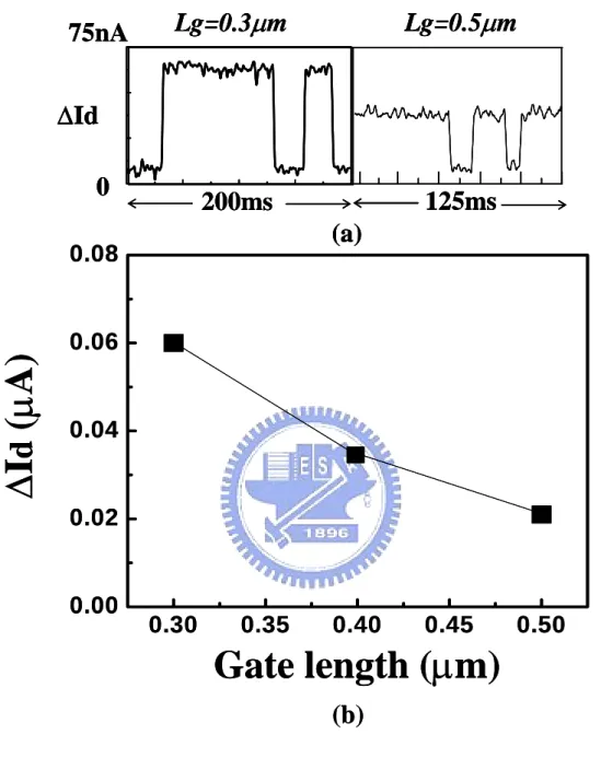
(52) 75nA. Lg=0.3µm. Lg=0.5µm. 200ms. 125ms. ∆Id 0. (a). ∆Id (µA). 0.08. 0.06. 0.04. 0.02. 0.00. 0.30. 0.35. 0.40. 0.45. 0.50. Gate length (µm) (b) Fig. 4.4. (a) Comparison of RTN amplitude for Lg=0.3µm and 0.5µm. (b) Dependence of ∆Id (two-level transition) on gate length. The read current level is about 1µA.. 42.
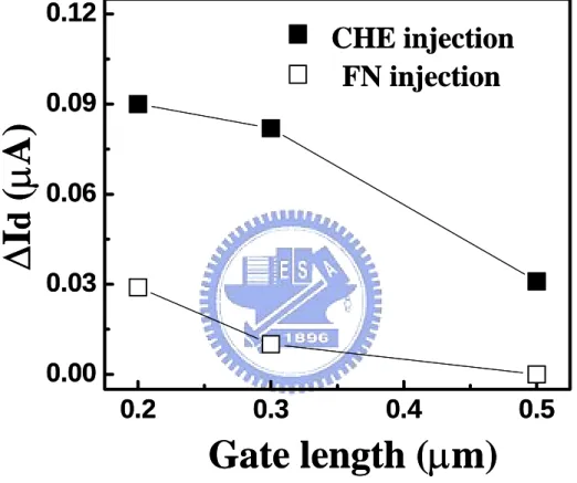
(53) 0.12. CHE injection FN injection. ∆Id (µA). 0.09 0.06 0.03 0.00 0.2. 0.3. 0.4. 0.5. Gate length (µm). Fig. 4.5. Calculated gate length dependence of two-level RTN amplitude from 2D device simulation. For CHE injection, the trapped charge width is assumed to be 30nm. FN injection has uniform charge storage. The parameters in simulation are not calibrated.. 43.
(54) 1.2. FN injection 1.1. ∆Id (µA). 1.0 1. 2. 3. 4. time (s) (a) 1.2. CHE injection 1.1 1.0 0. 50. 100. 150. 200. time (ms) (b). Fig. 4.6. Typical RTN traces for uniform FN injection (a) and channel hot electron injection (b). Both cells have the same P/E stress conditions.. 44.
(55) CHE injection, respectively. The two cells experience the same cycling procedure but have different injection conditions in the last programming. In the uniform FN injection cell (Fig. 4.6(a)), RTN is very small or undetectable in a measurement span of 4 seconds. The simulated result in Fig 4.5 also shows that uniform injection yields smaller RTN. Our result here is consistent with earlier work in [42] that non-uniform channel Vt-distribution can increase 1/f noise. Fig 4.7 shows the maximum read current fluctuation and corresponding number of levels in read current in a 0.3µm cell. The read current is about 30µA. At 100k P/E cycles, 5-level transitions in read current is noticed and maximum ∆Id is ~0.7µA in a sampling space of 105 reading. RTN with more levels and a large ∆Id is still expected as more reading are taken [43].. 4.5 Oxide Process Effect To evaluate bottom oxide process effect on RTN, two different oxide process conditions with a 0.5µm gate length (device A and device B) are used. Device B is known to have better oxide endurance from a charge pumping measurement result (Fig. 4.8(a)) RTN traces in device A and B are shown in Fig. 4.8. Note that device B exhibits smaller amplitude in read current fluctuation. This is because device B has less oxide traps creation and thus the probability of multi-level RTN is much reduced.. 45.
(56) 0 .8. Max. ∆Id (µA). Lg=0.3µm 0 .6. (a). 0 .4 0 .2 0. 10. Fig. 4.7. 103 P/E cycles. 105. Maximum ΔId observed at a read current of 30µA from multi-level RTN. The sampling size is 105 readings.. 46.
(57) (a). NROM. Process A. Process B. ∆Icp(10k). 70pA. 40pA. ∆Id (µA). 1.30 1.25 1.20. (b). 1.15 1.30 1.25 1.20 1.15. (c) 0. 20. 40. 60. 80. 100. 120. Time (ms) Fig. 4.8. (a) The increment of charge pumping current (Icp) in device A and device B after 10k P/E cycles. (b) RTN traces in Device A after 10k P/E cycles (c) RTN traces in Device B after 10k P/E cycles.. 47.
(58) Chapter 5 Conclusion In low-Vt state, P/E stress created positive oxide charge plays a major role in various reliability issues. ONO process is critical to the improvement of the cell reliability. High-Vt state charge retention in the major nitride flash cells, NROM, is investigated. Our result shows that the electron injection method has large impact on nitride charge retention behavior. Oxide charge trapping/detrapping induced read current fluctuation is discussed. Read current noise is increased in localized charge storage cells due to non-uniform Vt distribution. As the cycle number increases, the read current instability caused by RTN will become more severe. The improvement of bottom oxide reliability can significantly reduce this effect.. 48.
(59) Reference [1]. Herman E. Maes and Jan F. Van Houdt, “Silicon Scaling and its Consequences for Memory Technology,” Non-Volatile Semi. Memory Workshop, pp. 7-10, 2003.. [2]. H. C. Pao and O’Connell, “Memory Behavior of an MNS Capacitor,” Appl. Phys. Lett., Vol. 12, p. 260, 1968.. [3]. H. A. R. Wegener, A. J. Lincoln, H. C. Pao, M. R. O’Connel, and R. E. Oleksiak, “The. Variable. Threshold. Transistor,. A. New. Electrically-Alterable,. Non-destructive Read-only Storage Device”, IEEE IEDM Abstract, p. 420, 1967. [4]. L. A. Kasprzak, R. B. Laibowitz, and M. Ohring, “Dependence of the Si-SiO2 Barrier Height on SiO2 Thickness in MOS Tunnel Structures”, J. Appl. Phys., Vol. 48, p. 4281, 1977.. [5]. S. Lai, “Flash Memories: Where we are and where we are going”, IEDM Tech. Dig., pp. 971-973, 1998.. [6]. M. L. French and M. H White, “Scaling of Multidielectric Nonvolatile SONOS Memory Structures”, Solid-State Electronics, Vol. 37, p.1913, 1995. [7] Y. L. Yang, A. Purwar, and M. H. White, “Reliability Considerations in Scaled SONOS Nonvolatile Memory Devices”, Solid-State Electronics, Vol. 43, p.2025, 1999. [8] M. H. White, Y. L. Yang, A. Purwar and M. L. French, “A Low Voltage SONOS Nonvolatile Semiconductors Memory Technology”, Non-Volatile Semi. Memory Workshop, p. 52, 1996. [9] Y. L. Yang and M. H. White, “Charge Retention of Scaled SONOS Nonvolatile Memory Devices at Elevated Temperatures”, Solid-State Electronics, Vol. 44, p.949, 2000. [10] J. Bu and M. H. White, “Effects of Two-Step High Temperature Deuterium Anneals on SONOS Nonvolatile Memory Devices”, IEEE Elect. Dev. Lett., Vol. 22, p. 17, 2001. [11] B. Eitan, P. Pavan, I. Bloom, E. Aloni, A. Frommer, and D. Finzi, “NROM: A Novel Localized Trapping, 2–Bit Nonvolatile Memory Cell”, IEEE Elect. Dev.. 49.
(60) Lett., Vol. 21, pp. 543-545, 2000. [12]. B. Eitan, P. Pavan, and I. Bloom, “NROMTM – A New Technology for Non-Volatile Memory Products” Solid-State Electronics Vol. 46, pp. 1757-1763, 2002.. [13]. B. Eitan, “Non-Volatile Semiconductor Cell Utilizing Asymmetrical Charge Trapping”, U. S. Patent 5 768192, June 16, 1998.. [14]. M. K. Cho and D. M. Kim, “High Performance SONOS Memory Cells Free of Drain Turn-On and Over-Erase: Compatibility Issue with Current Flash Technology”, IEEE Elect. Dev. Lett., Vol. 21, p. 399, 2000.. [15]. M. White, “On the Go with SONOS,” IEEE Circuit and Device Magazine, pp.22-31, 2000.. [16]. W. J. Tsai, N. K. Zous, C. J. Liu, C. C. Liu, C. H. Chen, Tahui Wang, Sam Pan, Chih-Yuan Lu, and S. H. Gu, “Data Retention Behavior of a SONOS Type Two-Bit Storage Flash Memory Cell” IEDM Tech. Dig., pp. 719-722, 2001.. [17]. K. Yoshikawa, “RESEARCH CHALLENGES FOR NEXT DECADE FLASH MEMORIES”, IEDMS, pp. 11, 2000.. [18]. D. J. Dumin and J. Maddux, “Correlation of Stress-Induced Leakage Current in Thin Oxide with Trap Generation Inside the Oxide,” IEEE Trans. Elect. Dev., Vol. 40, pp986, 1993.. [19]. K. Lehovec and A. Fedotowsky, “A Charge retention of MNOS devices limited by Frenkel-Poole detrapping”, J. Appl. Phys., Vol. 32, pp. 335, 1978.. [20]. T. R. Oldham, A. J. Lelis, and F. B. Mclean, “Spatical dependence of trapped holes determined from tunneling analysis and measured annealing”, IEEE Trans. Nucl. Sci., Vol. NS-33, pp. 1203, 1986.. [21]. Shin-ichi Minami and Y. Kamigaki, “A novel MONOS nonvolatile memory device ensuring 10-year data retention after 107 erase/write cycles”, IEEE Trans. Elect. Dev., Vol. 40, pp 2001, 1993.. [22]. T. E. Chang, Investigation of Oxide-Damage-Induced Reliability Issues in VLSI MOSFET Devices by Using Transient Spectroscopic Techniques, Ph.D.. 50.
(61) Dissertation, Nation Chiao Tung University, 1997. [23]. M. Berger and J. Shappir, “Generations of interface states in electrically stressed and high temperature annealed MOS devices”, Proc. Electrical and Electronics Engineers, pp. 73, 1991.. [24]. S. M. Sze, “Current Transport and Maximum Dielectric Strength of Silicon Nitride Films”, J. Appl. Phys., Vol. 38, pp. 2951, 1967.. [25]. R. Rofan and C. Hu, “Stress-induced oxide leakage”, IEEE Elect. Dev. Lett., Vol. 12, pp. 632, 1991.. [26]. W. J. Tsai, S. H. Ku, N. K. Zous, C. J. Liu, C. C. Lu, C. H. Chen, T. Wang, Sam Pan, and C. Y. Lu, “Data Retention Behavior of a SONOS Type Two-Bit Storage Flash Memory Cell,” IEDM Tech. Digest, pp. 719-722, 2001.. [27]. T. Wang, N. K. Zous, J. L. Lai and C. Huang, “Hot hole Stress Induced Leakage Current (SILC) Transient in Tunnel Oxides,” IEEE Elect. Dev. Lett., Vol. 19, pp. 411-413, 1998.. [28]. C. Dunn, C. Kaya, T. Lewis, T. Strauss, J. Schreck, P. Hefley, M. Middendorf, T. San, “FLASH EPROM DISTURB MECHANISMS”, Proc. Int. Reliability Phys. Symp., pp. 299, 1994.. [29]. S. Manzini and A. Modelli, “Tunneling discharge of trapped holes in silicon dioxide”, in Insulation Films on Semiconductors, J. F. Verwij and Wolters, Eds. Amsterdam, The Netherlands; Elsevier, pp. 112, 1983.. [30]. J. R Chelikowsky and M. Schluter, “Electron states in quartz: A self-consistent pseudopotential calculation,” Phys. Rev. B., Vol. 15, pp. 4020, 1997.. [31]. B. Brar. G. D. Wilk, and A. C. Seabaugh, “Direct extraction of the electron tunneling effective mass in ultrathin SiO2”, J. Appl. Phys., Vol. 69, pp. 2728, 1996.. [32]. F. J. Grunthaner, B. F. Lewis, N. Zamini, and J. Maserjian, “XPS studies of structure-induced radiation effects at the Si/SiOm interface”, IEEE Trans. Nucl. Sci., Vol. NS-27, pp. 1640, 1980.. 51.
(62) [33]. T. Wang, N. K. Zous, J. L. Lai ,and C. Huang, “Hot Hole Stress Induced Leakage Current Transient in Tunnel Oxides”, IEEE Elect. Dev. Lett., Vol. 19, pp. 411, 1998.. [34]. W. J. Tsai, C. C. Yeh, N. K. Zous, C. C. Liu, S. K. Cho, C. H. Chen, Tahui Wang, Sam Pan, and Chih-Yuan Lu, “Hot Carrier Enhanced Read Disturb and Scaling Effects in a Localized Trapping Storage SONOS Type Flash Memory Cell,” Int. Conf. on Solid State Devices and Materials , pp. 164-165, 2002.. [35]. T. Endoh, H. Lizuka, S.Aritome, and F. Masuoka, “New Write / Erase Operation Technology for Flash EEPROM Cells to Improve the Read Disturb Characteristics,” IEDM Tech. Digest, pp. 603-606, 1992.. [36]. C. C. Yeh, W. J. Tsai, S. K. Cho, Tahui Wang, Sam Pan, and Chih-Yuan Lu, “A Modified Read Scheme to Improve Read Disturb and Second Bit Effects in a Scaled MXVAND Flash Memory Cell,” Non-Volatile Semi. Memory Workshop, pp. 44-45, 2003.. [37]. Eli Luskey, Yosi Shacham-Diamand, Ilan Bloom, and Boaz Eitan, “Electron Retention Model for Localized charge in Oxide-Nitride-Oxide(ONO) dielectric,” IEEE Elect. Dev. Lett., Vol. 23, pp. 556-558, 2002.. [38]. J. M. Shannon, B. A. Morgan, “Hole Transport via Dangling - Bond States in Amorphous Hydrogenated Silicon Nitride,” J. of Appl. Phys., Vol. 86, pp. 1548-1551, 1999.. [39]. W. J. Tsai, S. H. Gu, N. K. Zous, C. C. Yeh, C. C. Liu, C. H. Chen, T. Wang, S. Pan, and C. Y. Lu, “Cause of Data Retention Loss in Nitride-Based Localized Trapping Storage Flash Memory Cells,” Proc. Int. Reliability Phys. Symp., pp. 34-38, 2002.. [40]. K. K. Hung, P. K. Ko, Chenming Hu, and Yiu Chung Cheng, “Random Telegraph Noise of Deep-Submicrometer MOSFET’s,” IEEE Elect. Dev. Lett., Vol. 11, pp.90-92, 1990.. [41]. P.. Fang,. Kwok. K.. Hung,. Ping. 52. K.. Ko,. and. Chenming. Hu,.
(63) “Hot-Electron-Induced Traps Studied Through the Random Telegraph Noise,” IEEE Elect. Dev. Lett., Vol. 12, pp.273-275, 1991. [42]. Ming-Horn Tsai, Hirotaka Muto, and T. P. Ma, “Random Telegraph Signals Arising from Fast Interface States in Metal-SiO2-Si Transistors,” Appl. Phys. Lett., Vol. 10, pp. 1691-1693, 2001.. [43]. Ming-Horn Tsai, T. P. Ma, “The Impact of Device Scaling on the Current Fluctuation in MOSFET’s,” IEEE Trans. Electron Devices, Vol. 41, pp.2061-2068, 1994.. [44]. Ming-Horn Tsai, T. P. Ma, and Terence B. Hook, “Channel Length Dependence of Random Telegraph Signal in Sub-Micron MOSFET’s,” IEEE Elect. Dev. Lett., Vol. 15, pp.504-506, 1994.. [45]. Jun-Wei Wu, J. C. Kuo, Kai-Lin Chiu, Chih-Chang Cheng, W. Y. Lien, G. W. Huang, and Tahui Wang, “Modeling of Pocket Implant Effect on Drain Current Flicker Noise in High Performance Analog CMOS Devices,” Ext. Abst. Conf. Solid State Devices and Materials, pp. 416-417, 2003.. [46]. Akiko Ohata, Akira Toriumi, Masao Iwase, and Kenji Natori, “Observation of Random Telegraph Signals: Anomalous Nature of Defects at the Si/SiO2 Interface,” J. Appl. Phys., Vol. 6, pp. 200-204, 1990.. 53.
(64) 簡. 歷. 姓名: 馬煥淇 性別: 男 生日: 民國 70 年 1 月 11 日 籍貫: 台灣台南市 地址: 台南市西門路二段 63 號 學歷: 國立交通大學電子工程學系. 88.9-92.6. 國立交通大學電子工程研究所碩士班 92.9-94.6 碩士論文題目:. 氮化矽快閃記憶元件可靠性量測與分析. SONOS Flash EEPROM Reliability Physics and Characterization. 54.
(65)
數據

+7
Outline
相關文件
In section29-8,we saw that if we put a closed conducting loop in a B and then send current through the loop, forces due to the magnetic field create a torque to turn the loopÆ
Assuming that the positive charge of the nucleus is distributed uniformly, determine the electric field at a point on the surface of the nucleus due to that
magnetic field lines that pass through the loop is
Monopolies in synchronous distributed systems (Peleg 1998; Peleg
using tungsten single crystal emitters the thermally-assisted Schottky type, using emitters of zirconium oxide. field emission
y A stochastic process is a collection of "similar" random variables ordered over time.. variables ordered
Microphone and 600 ohm line conduits shall be mechanically and electrically connected to receptacle boxes and electrically grounded to the audio system ground point.. Lines in
Pursuant to the service agreement made between the Permanent Secretary for Education Incorporated (“Grantor”) and the Grantee in respect of each approved programme funded by the
