This article was downloaded by: [National Chiao Tung University 國立交 通大學]
On: 28 April 2014, At: 05:53 Publisher: Taylor & Francis
Informa Ltd Registered in England and Wales Registered Number: 1072954 Registered office: Mortimer House, 37-41 Mortimer Street, London W1T 3JH, UK
International Journal of
Electronics
Publication details, including instructions for authors and subscription information: http://www.tandfonline.com/loi/tetn20
A self-correction Hopfield
neural network for
computing the bit-level
transform image coding
PO-RONG CHANGPublished online: 10 Nov 2010.
To cite this article: PO-RONG CHANG (1997) A self-correction Hopfield neural network for computing the bit-level transform image coding, International Journal of Electronics, 83:2, 215-234, DOI: 10.1080/002072197135544 To link to this article: http://dx.doi.org/10.1080/002072197135544
PLEASE SCROLL DOWN FOR ARTICLE
Taylor & Francis makes every effort to ensure the accuracy of all the information (the “Content”) contained in the publications on our platform. However, Taylor & Francis, our agents, and our licensors make no representations or warranties whatsoever as to the accuracy, completeness, or suitability for any purpose of the Content. Any opinions and views expressed in this publication are the opinions and views of the authors, and are not the views of or endorsed by Taylor & Francis. The accuracy of the Content should not be relied upon and should be independently verified with primary sources of information. Taylor and Francis shall not be liable for any losses, actions, claims, proceedings, demands, costs, expenses, damages, and other liabilities whatsoever or howsoever caused arising directly or indirectly in
reselling, loan, sub-licensing, systematic supply, or distribution in any form to anyone is expressly forbidden. Terms & Conditions of access and use can be found at http://www.tandfonline.com/page/terms-and-conditions
A self-correction Hopfield neural network for computing the bit-level
transform image coding
PO-RONG CHANG²
A Hopfield-type neural network approach is presented, which leads to an analogue circuit for implementing the bit-level transform image. Unlike the conventional digital approach to image coding, the analogue coding system would operate at a much higher speed and it requires less hardware than a digital system. To utilize the concept of neural net, the computation of a two-dimensional DCT-based transform coding should be reformulated as minimizing a quadratic nonlinear programming problem subject to the corresponding 2s complement binary variables of two-dimensional DCT coefficients. A Hopfield-type neural net with a number of graded-response neurons designed to perform the quadractic nonlinear programming would lead to such a solution, in a time determined by
RC time constants, not by algorithmic time complexity. Nevertheless, the existance
of local minima in the energy function of the original Hopfield model implies that in general the correct globally optimal solution is not guaranteed. To tackle this difficulty, a network with an additional self-correction circuitry is developed to eliminate these local minima and yields the correct digital representations of 2-D DCT coefficients. A fourth-order Runge± Kutta simulation is conducted to verify the performance of the proposed analogue circuit. Experiments show that the circuit is quite robust and independent of parameter variations, and the computation time of an 8´ 8 DCT is estimated as 128 ns for RC= 10-9.
1. Introduction
The goal of transform image coding is to reduce the bit-rate to minimize com-munication channel capacity or digital storage memory requirements while main-taining the necessary fidelity of data. The discrete cosine transform (DCT
)
has been widely recognized as the most effective among various transform coding methods for image and video signal compression. However, it is computationally intensive and is very costly to implement using discrete components. Many investigators have explored ways and means of developing high-speed architectures for real-time image data coding (Sun et al. 1987, Liou and Bellisio 1987)
. Up to now, all image coding techniques, without exception, have been implemented by digital systems using digital multipliers, adders, shifters and memories. As an alternative to the digital approach, an analogue approach based on a Hopfield-type neural network (Hopfield 1984, Tank and Hopfield 1986)
is presented.Neural network models have received more and more attention in many fields where high computation rates are required. Hopfield and Tank showed that the neural optimization network can perform some signal-processing tasks, such as the signal decomposition/decision problem. Culhane et al. (1989
)
applied their con-cepts to discrete Hartley and Fourier transforms. Chua and Lin (1988)
and Chang etal. (1991
)
proposed an analogue approach based on Hopfield neural network to0020± 7217/97 $12.00Ñ 1997 Taylor & Francis Ltd.
Received 21 November 1996; accepted 16 December 1996.
² Department of Communication Engineering, National Chiao-Tung University,
Hsin-Chu, Taiwan, Republic of China. Fax: + 886 35 710116; e-mail:[email protected].
implement the two-dimensional (2-D
)
DCT transform. Chang et al. (1991)
demon-strated that the computation time for the 2-D DCT transform is within the RC time constants of the neural analogue circuit. Owing to the nature of the energy function of the Hopfield neural network, the solution of this network is highly dependent on its initial state. The energy function may decrease to settle down at one of the equilibrium points called `spurious states’ or local minima that does not correspond to the exact digital representations of the 2-D DCT coefficients. Moreover, Lee and Sheu (1988, 1989)
investigated the conditions for determining the local minima and detailed analysis on the equilibrium properties of Hopfield networks. Simulated annealing (Kirkpatrick et al. 1983)
is one heuristic technique to help escape the local minima by perturbing the energy function with the annealing temperature and artificial noise. It is proven that the solution obtained by the simulated annealing is independent of the initial state and is very close to the global minimum. As the network should settle down at each temperature and the temperature decrement is very small, an extraordinary long time is required in the computation and it does not meet the real-time requirement. A different approach to eliminating the local minima has been proposed by Lee and Sheu (1989)
. Their method is based on adding an additional self-correction circuitry to the original Hopfield network, and it yields the global minimum in real time. Here we use Lee and Sheu’s concept in our design.In this paper a neural-based optimization formulation is proposed to solve the two-dimensional (2-D
)
discrete cosine transform in real time. It is known that the direct computation of a 2-D DCT of size L´
L is to perform the triple matrixproduct of an input image matrix and two orthonormal base matrices. After proper arrangements, the triple matrix product can be reformulated as minimizing a large-scale quadratic nonlinear programming problem subject to L
´
L DCT coefficientvariables. However, a decomposition technique is applied to divide the large-scale optimization problem into L
´
L smaller-scale subproblems, each of which dependson its corresponding 2-D DCT coefficient variable only and then can be easily solved. To achieve the digital video applications, each 2-D DCT coefficient variable should be considered in the 2s complement binary representation. Therefore, each subproblem has been changed to be a new optimization problem subject to a number of binary variables of the corresponding 2-D DCT coefficient. Indeed, the new optimization problem is also a quadratic programming with minimization which occurs on the corners of the binary hypercube space. This is identical to the energy function involved in the Hopfield neural model (Hopfield 1984, Tank and Hopfield 1986
)
. They showed that a neural net has associated with it an `energy function’ which the net always seeks to minimize. As the energy function of Hopfield model has many local minima, the network output is usually the closest local minimum to the initial state which may be not identical to the desired DCT coefficient. A self-correction circuitry for the neural-based DCT transform coder is developed in § 5 to improve the probability of finding the correct global minimum solution. With the extra self-correction logic, the energy function decreases until the net reaches a steady-state solution (global minimum point which is the desired 2-D DCT coeffi-cient. Experimental results shown in § 7 have been conducted to verify the perfor-mance of the self-correction neural network. It is seen that the architecture of the neural net designed to perform the 2-D DCT would, therefore, reach a solution in a time determined by RC time constants, not by algorithmic time complexity, and would be straightforward to fabricate.2. An optimization formulation for the transform image coding
The Discrete cosine transform (DCT
)
is an orthogonal transform that consists of a set of basis vectors that are sampled cosine functions A normalized L th-order DCT matrixUis defined by ust=( )
2L 1 /2 cos p(
2s+1)
t 2L[
]
(
1)
for 0
£
s£
L-
1,
1£
t£
L-
1 and ust= L-1 /2 for t=0. The two-dimensional(2-D
)
DCT of size L´
L is de® ned asY= UTXU
(
2)
whereUT is the transpose ofU, andXis the given image data block of size L
´
L(typically 8
´
8 or 16´
16)
.Traditionally, the resultant matrix in the transform domainYmay be obtained by a direct implementation of (2
)
which is computationally intensive. By taking the advantage of the high-speed analogue implementation of the Hopfield-type neural network (Hopfield 1984, Tank and Hopfield 1986)
, the following formulations are required and would be described as follows.From (2
)
, we have X= UYUT =å
L-1 i=0å
L-1 j=0 yijuiuTj(
3)
where yij denotes the
(
i,
j)
entry of Yandui is the ith column vector of U.Define the distance or norm between two matricesAandBto be
NORM
(
A,
B)
= tr(
ATB)
(
4)
where tr(
A)
is equal toå
iL=-01aii.LetD = X
-
UYUTand||
D||
2= NORM(
D,
D)
. Therefore, the coefficients yijin(3
)
minimize the distance function minyij0£ i,j£ L-1
||
D||
2(
=||
X-
UYUT||
2)
(
5)
In this way, givenX, the problem of computingYby (3
)
has been changed intothe problem of finding the minimumY=
[
yij]
of the function||
D||
2 in (5)
.To reduce the complexity of performing the optimization problem in (5
)
,||
D||
2can be rewritten in the following form:
||
D||
2=å
L-1 i=0å
L-1 j=0||
X-
yijuiuTj||
2-
(
L2-
1)
tr(
XTX)
(
6)
Observing (6
)
, it should be noted that the second term of the right-hant side of (2)
is constant, and the components involved in the summation of the ® rst term are inde-pendent of each other. Therefore, the minimization problem (5)
could be divided intoL2subproblems as follows: miny
ij
||
D ij||
2
(
=||
X
-
yijuiuTj||
2)
,
0£
i,
j£
L-
1(
7)
Indeed, (7
)
can be expanded and rearranged in the scalar form miny ij||
D ij||
2 =å
Ls=-01å
L-1 t=0(
xst-
yijuisutj)
2(
)
(
8)
This decomposition approach provides us with a technique to divide a large-scale optimization problem into a number of smaller-scale subproblems, each of which can be easily solved.
Owing to the requirement of many digital video applications, each yijis quantized
into ^yij which can be represented by the 2s complement codes as follows:
^yij=
-
s(ijmij)2mij+å
mij-1
p=-nij
s(ijp)2p
(
9)
where s(ijp) is the pth bit of ^yij which has a value of either 0 or 1; s(ijmij-1) is the most
signi® cant bit (MSB
)
, s(-nij)ij is the least signi® cant bit, and s
(mij)
ij is the sign bit.
By substituting (9
)
into (8)
, one may obtain the new minimization problem subject to the binary variables, s(ijp)= 0 or 1,-
nij£
p£
mij; that ismin
s(ijp)
-nij£ p£mij
||
D ij||
2(
10)
In the following section a novel neural-based optimizer is proposed to solve the above minimization problem, to meet the real-time requirement of many digital video applications.
3. A neural-based optimization approach
Artificial neural networks contain a large number of identical computing ele-ments or neurons with specific interconnection strengths between neuron pairs. The massively parallel processing power of neural network in solving difficult problems lies in the cooperation of highly interconnected computing elements. It is shown that the speed and solution quality obtained when using neural networks for solving specific problems in signal processing make specialized neural network implementa-tions attractive. For instance, the Hopfield network can be used as an efficient technique for solving various combinatorial problems (Hopfield and Tank 1985
)
by the programming of synaptic weights stored as a conductance matrix.The Hopfield model is a popular model of continuous interconnected N nodes. Each node is assigned a potential, up
(
t)
,
p= 1,
2,
. . .,
N, as its state variable. Eachnode receives external input bias Ip
(
t)
and internal inputs from other nodes in theform of a weighted sum of firing rates
å
qTpqgq(
¸quq), where gq(
´)
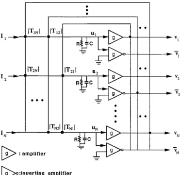
is amono-tonically increasing sigmoidal bounded function converting potential to firing rate. The general structure of the networks is shown in Fig. 1. The equations of motion are Cdup dt =
-up R+å
N q=1 Tpqvq+Ip vp= gp(
¸pup)(
11)
where ¸p are the ampli® er gains and gp
(
¸pup) is typically identi® ed as1
2
(
1+tanh¸pup)).Electrically, Tpqvqmight be understood to represent the electrical current input to
neuron p due to the present potential of neuron q. The quantity
|
Tpq|
represents thefinite conductance between the output vq and the body of neuron p. In other words,
this connection is made with a resistor of value Rpq= 1 /
|
Tpq|
. If Tpq>
0 this resistoris conducted to the normal output of amplified q. If Tpq
<
0 it is conducted to theinverted output of amplifier q. It would also be considered to represent the synapse efficacy. The term
-
up/R is the current flow due to finite transmembrane resistanceR, and it causes a decrease in up. Ipis any other (fixed
)
input bias current to neuron p.Thus, acording to (11
)
, the change in upis due to the changing action of all the Tpqvqterms, balanced by the decrease due to
-
upR, with a bias set by Ip.Hopfield and Tank have shown that in the case of symmetric connections
(
Tpq= Tqp)
, the equations of motion for this network of analogue processors alwayslead to a convergence to stable states, in which the output voltages of all amplifiers remain constant. In addition, when the diagonal elements
(
Tpp)are 0 and the ampli-fier gains¸pare high, the stable states of a network composed of N neurons are theminima of the computational energy of Lyapunov function
E=
-
1 2å
N p=1å
N q=1 Tpqvpvq-
å
N p=1 Ipvp(
12)
Figure 1. The circuit schematic of Hopfield model. Black squares at intersections represent resistive connections (
|
Tpq|
). If Tpq<0, the resistor is connected to the invertedamplifier.
The state space over which the analogue circuit operates is the N-dimensional hypercube defined by vp= 0 or 1. However, it has been shown that in the high-gain
limit networks with vanishing diagonal connections
(
Tpp= 0)
have minima only atcorners of this space (Tank and Hopfield 1986
)
. Under these conditions the stable states of the network correspond to those locations in the discrete space consisting of the 2Ncorners of this hypercube which minimize E.To solve the minimization problem in (10
)
by the Hopfield-type neural network, the binary variables s(ijp)should be assigned to their corresponding potential variablesupwith N
(
= mij+nij+1)
neurons. Truly, the computational energy function Eijofthe proposed network for yij may be identified as
||
D ij||
2in (10)
. However, with thissimply energy function there is no guarantee that the values of s(ijp) will be near
enough to 0 or 1 to be identified as digital logic. As (10
)
contains diagonal elements of theT-matrix that are non-zero, the minimal points to the||
D ij||
2 in (10)
will notnecessarily lie on the corners of the hypercube, and thus may not represent the exact 2s complement digital representation. One can eliminate this problem by adding one additional term to the function
||
D ij||
2. Its form can be chosen asD Eij=
å
L-1 s=0å
L-1 t=0å
mij p=-nij s(ijp)(
1-
s(ijp))
22pé
ë
ù
û
(
uis)2(
utj)2ì
í
î
ü
ý
þ
(
13)
The structure of this term was chosen to favour digital representations. Note that this term has the minimal value when, for each p, either s(ijp)= 1 or s(ijp)= 0. Although
any set of (negative
)
coef® cients will provide this bias towards a digital representa-tion, the coef® cients in (13)
were chosen to cancel out the diagonal elements in (10)
. The elimination to diagonal connection strengths will generally lead to stable points only at corners of the hypercube. Thus the new total energy function Eijfor yijwhichcontains the sum of the two terms in (10
)
and (13)
has minimal value when the{
s(ijp)}
is a digital representation close to the resultant yij in (3
)
. After expanding andrearranging the energy function Eij, we have
Eij =
||
D ij||
2+ D Eij =-
1 2å
mij p=-nijå
mij q=-nij s(ijp)s(ijq)Tpqij-
å
mij p=-nij s(ijp)Ipij(
14 a)
where Tpqij = 0,
f or p=q-
2Lå
-1 s=0å
L-1 t=02 p+qu2 isu2tj,
f or p /=q,
p /=mij,
q /=mij 2Lå
-1 s=0å
L-1 t=02 p+qu2 isu2tj,
f or p /=q,
p /=mij,
q=mij 2Lå
-1 s=0å
L-1 t=02 p+qu2 isu2tj,
f or p /=q,
p=mij,
q /=mijì
ïïïïï
ïïïï
í
ïïïïï
ïïïï
î
(
14 b)
Ipij=
å
L-1 s=0å
L-1 t=0(
2 p+1u isutjxst-
22pu2isu2tj),
f or p /=mij-
Lå
-1 s=0å
L-1 t=0(
2 p+1u isutjxst+22pu2isu2tj),
f or p=mijì
ïïï
í
ïïï
î
(
14 c)
As it can be shown that the term
(
å
sL=-01å
tL=-01u2isu2tj) is identical to unity for0
£
i,
j£
L-
1, (14 b)
and (14 c)
become Tpqij = 0,
f or p=q-
2p+q+1 f or p /=q,
p /= mij,
q /=mij 2p+q+1 f or p /= q,
p /= mij,
q=mij 2p+q+1 f or p /=q,
p= m ij,
q /=mijì
ïï
í
ïï
î
(
15 a)
Ipij= 2 p+1v s(ij)+22pVR,
f or p /=mij-
2p+1v s(ij)+22pVR,
f or p= mij{
(
15 b)
where vs(ij)is the analogue input voltage and it equals
(
å
sL=-01å
tL=-01uisutjxxt), and VRis the reference voltage and it equals 1 V.
Observing (15 a
)
, it may be found that the synapse weights Tpqij do not include theindex
(
i,
j)
of their corresponding results yij directly. Meanwhile, the range of Tpqijdepends on the
(
i,
j)
-related parameters mijand nijinherently. Moreover, the energyfunction for the simple Hopfield neural-based transform coding circuitry shown in Fig. 2 can be rewritten as
E=
-
1 2å
m p=-nå
m q=-n Tpqvpvq-
å
m p=-n(
TpRVR+ TpsVs)vp(
16)
where vp corresponds to s(ijp), and TpR is the conductance between the pth ampli® er
and the reference voltage VR, and Tps is the conductance between the pth ampli® er
input and analogue input voltage. Note that the index
(
i,
j)
is not included in (16)
for the sake of simplicity. The values for TpRand Tps are given byTpR= 22p
(
17 a)
Tps= 2
p+1
,
f or-
n£
p£
m-
1-
2p+1,
f or p=m{
(
17 b)
The corresponding circuit dynamics of the simple Hopfield neural-based transform coding can be described as
Cdup dt =
-
TpR+ Tps+å
m q=-n Tpq(
)
up+å
m q=-n Tpqvq+ TpRVR+ TpsVs vp =gp(
¸pup)
(
18)
4. Local minima of Hopfield neural-base d transform coding
Lee and Sheu (1988, 1989
)
showed that the energy function of a Hopfield net-work has many local minima and the resultant netnet-work output is the closest local minimum to the initial state. The existance of local minima in the energy function of the Hopfield network is not tolerable for a great variety of engineering optimization applications. In this section we discuss the properties of the local minima of neural-based transform image coding.At a stable point, the term
(
C dup/dt)
of (18)
becomes zero and every neuroninput voltage is governed by
up
>
<
0 when v0 when vp= 1 Vp= 0
{
(
19)
From (18
)
and (19)
, the range of input voltage Vs to the pth amplifier for thecorresponding stable state and a specific digital output can be calculated:
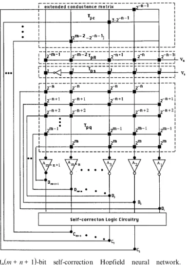
Figure 2. An(m+n+1
)
-bit self-correction Hopfield neural network. Di= vi-n-1Â1£ i£ m+n+1 and Cl= fl-n-1(V-n
,
. . . Vm)
,
2£ l£ m+n.Vs
>
-
TpR Tps( )
VR-
å
m q=-n Tpq Tps( )
vq,
when vp= 1 V and-
n£
p£
m-
1<
-
TmR Tms( )
VR-
å
m-1 q=-n Tmq Tms( )
vq,
when vm=1 Vì
ïïïï
í
ïïïï
î
ü
ïïïï
ý
ïïïï
þ
(
20 a)
Vs<
-
TpR Tps( )
VR-
å
m q=-n Tpq Tps( )
vq,
when vp=0 and-
n£
p£
m-
1>
-
TmR Tms( )
VR-
å
m-1 q=-n Tmq Tms( )
vq,
when vm=0ì
ïïïï
í
ïïïï
î
ü
ïïïï
ý
ïïïï
þ
(
20 b)
Substitute (15 a)
, (17 a)
and (17 b)
into (20 a)
and (20 b)
; this yieldsVs
>
2p-1+å
m q=-n 2qvq-
vm2m,
when vp= 1 V and-
n£
p£
m-
1<
-
2m-1+å
m-1 q=-n 2qvq,
when vm=1 Vì
ïïïï
í
ïïïï
î
ü
ïïïï
ý
ïïïï
þ
(
21 a)
Vs<
2p-1+å
m-1 q=-n 2qvq-
vm2m,
when vp= 1 V and-
n£
p£
m-
1>
-
2m-1+å
m-1 q=-n 2qvq,
when vm= 0ì
ïïïï
í
ïïïï
î
ü
ïïïï
ý
ïïïï
þ
(
21 b)
During the transient period, the voltage vp is changing in the direction that the
energy function E decreases. When all amplifiers reach the stable condition in (19
)
, a local minimum is reached and the searching process is terminated. The inequalities (21 a)
and (21 b)
are derived for the pth amplifier output voltage to be stable. For a stable output, the input voltage range is given by the logic-AND operation of the range decided by each amplifier. From (21 a)
and (21 b)
, it is indicated that the lower limit and upper limit of Vsare determined by the first high-bit occurrence andlow-bit occurrence of the digital code from the least significant low-bit (LSB
)
, respectively. In other words, if a digital code has the first low bit at the pth bit, the next adjacent digital code has the first high bit at the pth bit. Thus, the upper limit and lower limit of input voltage between the two adjacent digital codes are decided by the pth amplifier.To justify the behaviour of local minima, a characteristic parameter GAPp
pro-posed by (Lee and Sheu 1988, 1989
)
is used as an indicator of the existance of local minima. The parameter GAPp is defined by the input voltage of the lower limit forvp= 1 V and the upper limit for vp =0 decioded by the pth amplifier
GAPp=
-
å
m q=-n Tpq Tps( )
(
vuq-
vlq),
f or-
n£
p£
m-
1-
må
-1 q=-n Tmq Tms( )
(
vlq-
vuq),
f or p= mì
ïïï
í
ïïï
î
(
22)
where vup and vlp are the pth ampli® er output voltages of the digital codes whose pth
bits from the least signi® cant bit (LSB
)
are logic 1 and logic 0, respectively.{
vuq}
and{
vlq}
are usually the adjacent digital codes and are given byvuq= vlq
,
if q>
p vuq= 1 V and vlq= 0,
if q=p vuq= 0 and vlq=1 V,
if q<
pü
ïï
ý
ïï
þ
(
23)
As GAPp represents the overlapped range of the input voltage Vs to the pth
amplifier, both adjacent digital codes can be stable and become the same converted output at a given input voltage. To guarantee that one of the adjacent digital codes is not a local minimum when the other code is the global minimum at a given input, the input voltage ranges for the codes should not be overlapped, i.e. GAPp
³
0 for everyp. The only global minimum corresponds to each analogue input. Hence, the
one-to-one correspondence between the digital output and analogue input should exist. Let us examine the existance of local mimina in neural-based transform coding. By substituting (23
)
into (22)
we haveGAPp=
-
2p+2-n
,
f or-n
£
p£
m-
12m
-
2-n,
f or p=m{
(
24)
Equation (24
)
shows that the indicator GAPpis always negative except when p=-
nand p= m. Thus, there could exist more than two digital output codes (i.e. local
minima
)
corresponding to a given analogue input for-
n<
p<
m. In the nextsec-tion a self-correcsec-tion logic based on Lee and Sheu’s concept is proposed to eliminate the overlapped input range.
5. Self-correction logic approach
The overlapped input voltage range between two digital codes can be eliminated by adding a correction logic circuitry at the amplifier (neuron
)
outputs as shown in Fig. 2. The values of conductances located in the main body of the neural network and the extended conductance network will be discussed and specified by (31)
± (34)
. Here we give the overall structure to understand the function of correction logic circuitry. The correction logic monitors the Hopfield network outputs and generates the correcting information. The correction voltage outputs are fed back into the neuron inputs through the extended conductance network. Note that there is no feedback connection to the input of the first amplifier (i.e. A1)
because the digital code decided by the first amplifier does not produce a local minimum for any analogue input signal. Similarly, there is no connection to the last amplifier (i.e.Am+n+1
)
.The correction logic circuitry and extended conductance network can be identified by using the following equation:
TpR+ Tps+ Tpc+
å
m q=-n q=/p Tpqæ
è
ö
ø
up = TpRVR+ TpsVs+ Tpcfp(
Vo)+å
m q=-n q=/p Tpqvq(
25)
where Vo is the digital output voltage given as
{-
vm2m+å
qm=--1nvq2q}
, fp(
Vo) is thepth correction logic output, Tpc is a conductance in the extended conductance
network to the pth ampli® er, and VR=
-
1 V.Using the procedure shown in the preceding section to derive the characteristic parameter, the indicator GAPp can be calculated:
GAPp=
-
2p+2-n-
Tpc2p+1
( )
(
fp(
Vo)l-
fp(
Vou))
,
f or-
n<
p<
m(
26)
where Voland Vouare the digital output voltages of the adjacent digital coded de® ned
in (23
)
, and they can be given byVl o=
-
Vml2m+å
m-1 q=-n Vl q2q(
27 a)
Vou=-
Vmu2m+å
m-1 q=-n Vqu2q(
27 b)
Note that only the characteristic parameters GAPp
, -
n<
p<
m, are consideredin designing the correction logic circuitry.
The local minima are eliminated when the indicators GAPp
, -
n<
p<
m, are setto be zero. Therefore, the extended conductance becomes
Tpc = 2
2p+1
-
2p+1-nfp
(
Vou)
-
fp(
Vo)l(
28)
As Tpc is always non-negative, the correction logic circuitry output can be
selected as fp
(
Vou)
=-
fp(
Vo)l>
0(
29)
Thus, Tpc becomes Tpc= 2 2p-2p-n fp
(
Vou)
(
30)
To characterize the correction logic circuitry specified by (29
)
, the circuitry out-put can take a discrete value of-
1,
0, or 1 V to be compatible with the amplifier output voltage and the reference voltage. Table 1 lists the relationship between the amplifier outputs Di= vi-n-1, for 1£
i£
N, and the correction logic outputsCl =fl-n-1
(
Vo) for 2£
l£
N-
1, where Vo is the digital output voltage andN= m+n+1= 16. The self-correction circuitry characterized by Table 1 can be implemented by the simple combinational logic or SRAM memory devices.
As the input voltage
{
up}
is determined by the ratios of the conductances, thescaling factor to realize absolute conductance values can be used as an integrated-circuit design parameter. For example, the conductances are reduced by a scaling factor
|
Tps|
(
=2p+1)
and are given byTpq= 0
,
f or p= q-
2q,
f or p /=q,
p /= m,
q /= m 2q,
f or p /=q,
p= m,
q /= m 2q,
f or p /=q,
p /= m,
q= mì
ï
í
ï
î
(
31)
Tpc= 2p-1-
2-n-1(
32)
A m pl ifi er ou tp ut C or re ct io n lo gi c ou tp ut D16 D15 D14 D13 D12 D11 D10 D9 D8 D7 D6 D5 D4 D3 D2 D1 C15 C14 C13 C12 C11 C10 C9 C8 C7 C6 C5 C4 C3 C2 ´ ´ ´ ´ ´ ´ ´ ´ ´ ´ ´ ´ ´ ´ 0 1 0 0 0 0 0 0 0 0 0 0 0 0 0 +1 ´ ´ ´ ´ ´ ´ ´ ´ ´ ´ ´ ´ ´ ´ 1 0 0 0 0 0 0 0 0 0 0 0 0 0 0
-1 ´ ´ ´ ´ ´ ´ ´ ´ ´ ´ ´ ´ ´ 0 1 1 0 0 0 0 0 0 0 0 0 0 0 0 +1 0 ´ ´ ´ ´ ´ ´ ´ ´ ´ ´ ´ ´ ´ 1 0 0 0 0 0 0 0 0 0 0 0 0 0 0 -1 0 ´ ´ ´ ´ ´ ´ ´ ´ ´ ´ ´ ´ 0 1 1 1 0 0 0 0 0 0 0 0 0 0 0 +1 0 0 ´ ´ ´ ´ ´ ´ ´ ´ ´ ´ ´ ´ 1 0 0 0 0 0 0 0 0 0 0 0 0 0 0 -1 0 0 ´ ´ ´ ´ ´ ´ ´ ´ ´ ´ ´ 0 1 1 1 1 0 0 0 0 0 0 0 0 0 0 + 1 0 0 0 ´ ´ ´ ´ ´ ´ ´ ´ ´ ´ ´ 1 0 0 0 0 0 0 0 0 0 0 0 0 0 0 -1 0 0 0 ´ ´ ´ ´ ´ ´ ´ ´ ´ ´ 0 1 1 1 1 1 0 0 0 0 0 0 0 0 0 + 1 0 0 0 0 ´ ´ ´ ´ ´ ´ ´ ´ ´ ´ 1 0 0 0 0 0 0 0 0 0 0 0 0 0 0 -1 0 0 0 0 ´ ´ ´ ´ ´ ´ ´ ´ ´ 0 1 1 1 1 1 1 0 0 0 0 0 0 0 0 + 1 0 0 0 0 0 ´ ´ ´ ´ ´ ´ ´ ´ ´ 1 0 0 0 0 0 0 0 0 0 0 0 0 0 0 -1 0 0 0 0 0 ´ ´ ´ ´ ´ ´ ´ ´ 0 1 1 1 1 1 1 1 0 0 0 0 0 0 0 + 1 0 0 0 0 0 0 ´ ´ ´ ´ ´ ´ ´ ´ 1 0 0 0 0 0 0 0 0 0 0 0 0 0 0 -1 0 0 0 0 0 0 ´ ´ ´ ´ ´ ´ ´ 0 1 1 1 1 1 1 1 1 0 0 0 0 0 0 + 1 0 0 0 0 0 0 0 ´ ´ ´ ´ ´ ´ ´ 1 0 0 0 0 0 0 0 0 0 0 0 0 0 0 -1 0 0 0 0 0 0 0 ´ ´ ´ ´ ´ ´ 0 1 1 1 1 1 1 1 1 1 0 0 0 0 0 +1 0 0 0 0 0 0 0 0 ´ ´ ´ ´ ´ ´ 1 0 0 0 0 0 0 0 0 0 0 0 0 0 0 -1 0 0 0 0 0 0 0 0 ´ ´ ´ ´ ´ 0 1 1 1 1 1 1 1 1 1 1 0 0 0 0 +1 0 0 0 0 0 0 0 0 0 ´ ´ ´ ´ ´ 1 0 0 0 0 0 0 0 0 0 0 0 0 0 0 -1 0 0 0 0 0 0 0 0 0 ´ ´ ´ ´ 0 1 1 1 1 1 1 1 1 1 1 1 0 0 0 +1 0 0 0 0 0 0 0 0 0 0 ´ ´ ´ ´ 1 0 0 0 0 0 0 0 0 0 0 0 0 0 0 -1 0 0 0 0 0 0 0 0 0 0 ´ ´ ´ 0 1 1 1 1 1 1 1 1 1 1 1 1 0 0 + 1 0 0 0 0 0 0 0 0 0 0 0 ´ ´ ´ 1 0 0 0 0 0 0 0 0 0 0 0 0 0 0 -1 0 0 0 0 0 0 0 0 0 0 0 ´ ´ 0 1 1 1 1 1 1 1 1 1 1 1 1 1 0 + 1 0 0 0 0 0 0 0 0 0 0 0 0 ´ ´ 1 0 0 0 0 0 0 0 0 0 0 0 0 0 0 -1 0 0 0 0 0 0 0 0 0 0 0 0 ´ 0 1 1 1 1 1 1 1 1 1 1 1 1 1 1 + 1 0 0 0 0 0 0 0 0 0 0 0 0 0 ´ 1 0 0 0 0 0 0 0 0 0 0 0 0 0 0 -1 0 0 0 0 0 0 0 0 0 0 0 0 0 T ab le 1. T he in pu t± ou tp ut re la tio n fo r th e se lf-co rr ec tio n lo gi c w he n N =16 . ´ m ea ns `d on ’t ca re ’.TpR= 2p-1
(
33)
Tps=
{
-
11,
,
f orf or p-
=n£
mp£
m-
1(
34)
6. System architecture for neural-base d transform coding
Observing (15 b
)
, it is indicated that the bias is not fixed but depends on input analogue signal xst and the index(
i,
j)
of its corresponding result yij. From (31)
± (34)
,one may find that the synapse weights
(
Tpq), extended conductance(
Tpc),
TpR andTpsdo not include the index
(
i,
j)
directly. However, their ranges are determined bytwo
(
i,
j)
-related parameters mij and nij. Therefore, both synapse weights and biasshould be programmable to capture the information from the data set. Chang et al. (1991
)
proposed a reconfigurable hybrid MOS neural circuit including electrically programming synapses and bias to implement the transform coding. As the realiza-tion of programmable synapses seems quite complicated, our paper presents a nor-malization technique to force their ranges to be within a fixed interval. After performing the normlaization, the bias would be the only remaining(
i,
j)
-related term. In this paper a cost-effective design according to the normalization technique is developed to compute the transform coding.The normalization procedure can be performed by letting the conductances, i.e.
Tpq
,
TpR and Tps be reduced by a new scaling facter, 2p+mij+1. Thus, the normalizedconductances become Tpq = 0
,
f or p= q-
2q-mij,
f or p /=q,
p /=m ij,
q /=mij 2q-mij,
f or p /=q,
p=m ij,
q /=mij 2q-mij,
f or p /=q,
p /=m ij,
q /=mijì
ïï
í
ïï
î
(
35)
Tpc= 2p-mij-1-
2-mij-nij-1(
36)
TpR= 2p-mij-1(
37)
Tps= 2 -mij,
f or-
n ij£
p£
mij-
1-
2-mij,
f or p= m ij{
(
38)
It can be shown that the ranges of normalized terms 2q-mij and 2p-mij-1are within
the intervals
[
2-N+1,
1]
and[
2-N,
2-1]
, and 2-mij-nij-1equals 2-N, respectively, where-
nij£
p,
q£
mij, and N(
= mij+nij+1)
is the number of neurons. Therefore,Tpq
,
Tpc and TpR are totally independent of the index(
i,
j)
which corresponds tothe resultant ^yij and depends on the normalized index
(
p,
q)
, which corresponds tothe size of neural network (or number of bits involved in ^yij
)
. Unfortunately, theconductance between the pth neuron and analogue input voltage, Tps, becomes an
(
i,
j)
-related term which is in the term 2-mij after performing normalization. Toeliminate the dependence of index
(
i,
j)
, several arrangements should be considered in the expression of bias Ipij:Ipij = Tpsvs(ij)+ TpRVR = T^ps^vs(ij)+ TpRVR
(
39)
where ^ Tps=-
11,
,
f orf or p-
n=ijm£
p£
mij-
1 ij{
(
40)
^vs(ij)= 2-mijvs(ij) =å
L-1 s=0å
L-1 t=0 2-miju isutjxst =å
L-1 s=0å
L-1 t=0 uistjxst(
41)
uistj =2-mijuisutj,
0£
i,
j,
s,
t£
L-
1(
42)
Basically, the concept of the above arrangements is considered to combine the
(
i,
j)
-related terms 2-mij and uisutj together. This new term is denoted by uistj. As a
result, those conductances located in the self-correction neural network are indepen-dent of the index
(
i,
j)
. Based on the above discussion, a proposed system architec-ture and the function strucarchitec-tures of normalized self-correction neural network and analogue MOS vector multiplier are illustrated in Figs 3, 4 (a)
and 4 (b)
respectively.Figure 3. Architecture of image transform coding neural chip.
The
(
i,
j)
-related parameters uistj could be precomputed and are stored in the(
L2´
L2)
register file which is controlled by a refreshing counted with clock D t1. Note thatD t1 is defined as the sum ofD trefresh(= time for refreshing the bias)
andD tneural (= computation time for the neural network
)
. Although computing a parti-cular ^yij, those parameters should be converted to analogue form and then pumpedout from the register file to the analogue MOS vector multiplier. From (40
)
, the analogue input to the network ^vs(i,j) can be obtained by performing the analogueinner vector multiplication between two L2-tuple vectors
x=
[
x00 x10 . . . xL-1,L-1]
Tuij =
[
ui,0,0,j ui,1,0,j . . . ui,L-1,L-1,j]
TThe time for updating the bias would be dominated by the computation time for the
L2
´
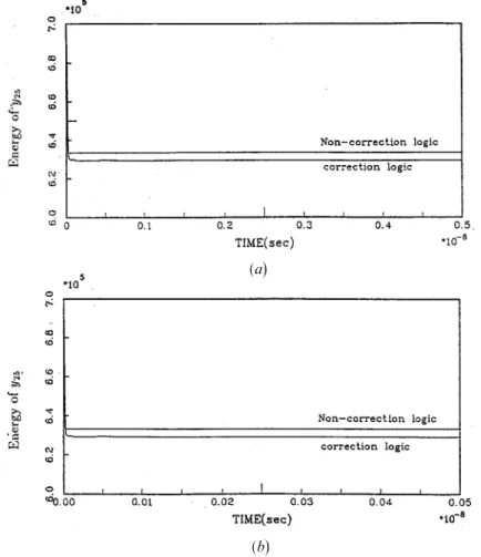
L2analogue inner vector multiplicationD tvm. In other words,D trefresh. D tvm.Figure 4. (a) The time evolution of the reduction of energy for y25 when RC= 10-9 and
¸= 105; (b)the time evolution of the reduction of energy for y25when RC= 10-10and
¸= 105.
(a)
(b)
As the L2 input analogue signals xst are required in computing the vector
multi-plication (with uistj
,
0£
s,
t£
L-
1)
involved in each Iijp,
0£
i,
j£
L-
1,
xst shouldstay in the analogue buffer until the L2^yijhave been completed. This analogue buffer
is controlled by a system counter with clock D t2=
(
L2(
D t1+ D toverhead))
, whereD toverhead is the time for input± output overhead. Usually, the analogue buffer if realized by analogue DRAM-style storage based on the ¯ oating-gate storage approach. The overall output of the analogue vector multiplier voutis given by
vout=
å
L-1 s=0å
L-1 t=0 cuistjxst(
43)
where c is the constant that depends on the characteristics of MOS implementation. It is interesting to note that the constant c could be compensated for by absorb-ing the values into uistj. For example, one may precompute the new uistj as c-1uistj,
where uistj is the old one. The input± output compatibility of the overall MOS
imple-mentation is of particular interest because the relatively high output impedance node of the double inveter is connected to the almost infinite input impedance node of the MOSFET gates with almost no restriction on the fan-in/fan-out cap-ability. More details about the analogue MOS vector multiplier are given by Mead (1989
)
, Salam et al. (1989)
and Khachab and Ismail (1987)
.7. Illustrated examples
To examine the performance of the neural-based analogue circuit for computing the 2-D DCT transform coding, an often used 8
´
8 DCT will be considered in our simulation because it represents a good compromise between coding efficiency and hardware complexity. Because of its effectiveness, the CCITT H.261 recommended standard for p´
64 kbit/s(
p= 1,
2,
. . .,
30)
visual telephony developed by CCITT, and the still-image compression standard developed by ISO JPEG all include the use of 8´
8 DCT in their algorithms.To obtain the size
(
N)
of neural network required to compute its corresponding DCT coefficient, it is necessary to calculate their respective dynamic range and take into account the sign bit. To achieve this purpose, the range of each DCT coefficient can be determined by generating random integer pixel data values in the range 0 to 255 through the 2-D discrete cosine transform. For example, the range of y00is from-
1024 to 1023. Therefore, m00 is identified as 11; that is, 10 bits are for the magni-tude of y00 and 1 bit is for the sign. As a result, the corresponding mij for each DCTcoefficient yij is illustrated in Table 2. Another important parameter required in
determining the size is nij, which depends on the required accuracy and the tolerable
mismatch in the final representation of the reconstructed video samples. The analysis of the accuracy and mismatch involved in the finite length arithmetic DCT compu-tation was discussed by Sun et al. (1987
)
and Liou and Bellisio (1987)
. Based on their results and the consideration of feasible hardware implementation, the number of bits (or size of neural network)
involved in each DCT coefficient is set to be 16. Thennij would be equal to
(
15-
mij), for example n00= 5. The above suggestion seemsquite reasonable to improve the accuracy of a particular yij which has a small
dynamic range.
We have simulated both the DCT-based neural analogue circuit without the correction logic of (18
)
, and a circuit based on the proposed correction logic usingthe simultaneous differential equation solver (DVERK in the IMSL
)
. This routine solves a set of nonlinear differential equations using the fifth-order Runge± Kutta method. It can be found that the convergence times for both neural networks is within the RC time constant. We used two different RC time constants,RC= 10-10
(
R= 1 kV,
C=0´01 pF)
and RC= 10-9(
R=1 kV,
C= 0´1 pF)
, and all amplifier gains¸p are assigned to be 104 in our experiments, and ran simulationson a SUN workstation. The test input pixel data xstare illustrated in Table 3 (a
)
. Figs4 (a
)
and (b)
show an example of the time evolution of the reduction of energy performed by both networks with N(
=16)
neurons that represent y25 based on the 2s complement binary number representation for two different RC time con-stants. Moreover, both figures show that the curves for correction logic case reach the steady-state values which are less than the values for the non-correction logic case. In other words, the non-correction reaches a local minimum and yields the incorrect solution. The (2,5)
-entry in Table 3 (c)
shows the resulting DCT coefficienty25obtained at the steady-state points on the correction logic curves of Figs 4 (a
)
and (b)
. It is shown that the result is almost independent of the RC time constants. However, each converegence time will be in proportion to its corresponding RC time constant. For example, the converge times for RC=10-10 and RC= 10-9 are in proportion to the orders of timescale 10-10s(
= 0´1 ns)
and 10-9s(
= 1 ns)
, respectively. However, these two curves have almost the same time evolution. Starting from a very high energy state, the neural network reduces its energy spon-taneously by changing its state so that the 2s complement binary variables s(ijp)minimize the error energy function.
Considering the system architeture shown in Fig. 3, another important module is the analogue vector multiplier. For simplicity in estimating the computation time in computer simulation, we assume that the op-amp involved in the overall MOS vector implementation is ideal. The computation time for a 64
´
64 analogue MOS vector multiplierD tvm is estimated as 1 ns by performing the inner vector product on two 64-tuple vectors on SPICE-II. Thus, the refreshing cloclD t1(
. D tneural+ D tvm)
is identified as 2 ns. Therefore, the computation time for computing all DCT coeffi-cients would be estimated as 128 ns when L= 8 and RC= 10-9. Computer simula-tion verifies the effectiveness of the proposed neural-based transform coder. Undoubtedly, this analogue coder can be practically implemented with ASICs using today’s low-cost VLSI technology. The estimated computation time provides an index to evaluate and justify the computational efficiency and performance of the real VLSI implementation of our design.i\ j 0 1 2 3 4 5 6 7 0 11 9 9 9 9 9 9 9 1 9 9 9 9 9 9 9 9 2 9 9 9 9 9 9 9 9 3 9 9 9 9 9 9 9 9 4 9 9 9 9 9 9 9 9 5 9 9 9 9 9 9 9 9 6 9 9 9 9 9 9 9 9 7 9 9 9 9 9 9 9 9 Table 2. mij for yij.
8. Conclusion
The computation of a 2-D DCT-based transform coding has been shown to solve a quadratic nonliner programming problem subject to the corresponding 2s comple-ment binary variables of 2-D DCT coefficients. We have shown that the existance of local minima in neural-based transform coding will lead to an incorrect digital representation of the DCT coefficient. A self-correction logic based on Lee and Sheu’s concept is developed to eliminate these local minima. Using this concept, a novel self-correction Hopfield-type neural analogue circuit designed to perform the DCT-based quadratic nonlinear programming could obtain the desired coefficients of an 8
´
8 DCT in 2s complement code within 128 ns with RC= 10-9.REFERENCES
CHANG, P. R., HWANG, K. S., and GONG, H. M., 1991, A high-speed neural analog circuit for
computing the bit-level transform image coding. IEEE Transactions on Consumer
Electronics,37, 337± 342.
CHUA, L. O., and LIN, T., 1988, A neural network approach to transform image coding.
International Journal of Circuit Theory and Applications,16, 317± 324.
CULHANE, A. D., PECKERAR, M. C., and MARRIAN, C. R. K., 1989, A neural net approach to
discrete Hartley and Fourier transform. IEEE Transactions on Circuits and Systems,
36, 695± 702. 0 981´25
-
31´97-
73´45 71´69 12´50 89´23 60´46-
60´00 1 34´81 39´81-
10´03 15´73 41´30 135´48-
97´65-
26´23 2-
24´38-
7´58 27´83 64´95-
49´14 12´92 145´73 93´47 3-
40´17-
40´78-
24´64-
15´38-
3´28-
136´39-
18´50-
5´27 4-
30´25 83´83-
64´59-
101´10 65´50-
31´25-
4´36 74´86 5-
72´70 26´72 42´30 134´44 38´60-
117´16-
43´08-
64´55 6 60´70-
47´47 23´98 71´83 13´32-
48´05-
165´58 55´75 7-
86´75 172´09 56´20 7´28 19´00 128´77 4´92 137´72Table 3. (a)Input pixel data xst; (b)corresponding DCT coefficients; (c)Neural-based DCT
coefficients. ()))) )) )) )) )) )) )) ))*, )) )) )) )) )) )) )) )) )) & (c
)
0 981´25-
31´98-
73´45 71´69 12´50 89´23 60´46-
60´00 1 34´81 39´82-
10´03 15´74 41´30 135´48-
97´65-
26´24 2-
24´38-
7´57 27´82 64´95-
49´14 12´93 145´73 93´48 3-
40´17-
40´78-
24´64-
15´38-
3´28-
136´40-
18´50-
5´26 4-
30´25 83´83-
64´59-
101´10 65´50-
31´25-
4´37 74´85 5-
72´70 26´73 42´29 134´43 38´60-
117´16-
43´07-
64´55 6 60´70-
47´46 23´98 71´82 13´32-
48´05-
165´57 55´75 7-
86´75 172´09 56´20 7´28 19´01 128´77 4´92 137´72 (b)
()))) )) )) )) )) )) )) ))*, )) )) )) )) )) )) )) )) )) & i\ j 0 1 2 3 4 5 6 7 0 159 87 86 105 172 105 103 55 1 126 17 194 230 28 238 179 128 2 253 105 48 181 103 94 255 26 3 73 159 29 241 138 175 66 145 4 120 74 220 201 97 5 87 70 5 2 187 10 118 203 252 162 209 6 160 56 97 19 53 221 14 78 7 131 31 233 85 140 168 118 126 (a)
()))) )) )) )) )) )) )) ))*, )) )) )) )) )) )) )) )) )) &HOLLER, M., TAM, S., CASTRO, H., and BENSON, R., 1989, An electrically trainable artificial
neural network (ETANN) with 10240 `Float gate’ synapses. International Joint
Conference on Neural Networks, Vol. 2, Washington DC, U.S.A., pp. 191± 196.
HOPFIELD, J. J., 1984, Neurons with graded response have collective computational properties
like those of two-state neurons. Proceedings of the National Academy of Science,
U.S.A.,81, 3088± 3092.
HOPFIELD, J., and TANK, D., 1985, Neural computations of decisions in optimization problems.
Biological Cybernetics,52, 141± 152.
KHACHAB, N., and ISMAIL, M., 1987, Novel continuous-time all-MOS four-quadrant
multipliers. Proceedings of the IEEE International Symposium on Circuits and
Systems (ISCAS), San Francisco, California, U.S.A., May, pp. 762± 765.
KIRKPATRICK, S., GELATT, C. D., Jr., and VECCHI, M. P., 1983, Optimization by simulated
annealing. Science,220, 650± 671.
LEE, B. W., and SHEU, B. W., 1988, An investigation on local minima of Hopfield Network for
optimization circuit. IEEE International Conference on Neural Networks, San Diego, California, U.S.A., Vol. 1, pp. 45± 51; 1989, Design of a neural-based A/D converter using modified Hopfield network. IEEE Journal of Solid-state Circuits,24, 1129± 1135;
1990, Parallel digital image restoration using adaptive VLSI neural chips. Proceedings
of the IEEE International Conference on Computer Design: V L SI in Computers and Processors, Cambridge, Massachusetts, U.S.A., 17± 19 September.
LIOU, M. L., and BELLISIO, J. A., 1987, VLSI implementation of discrete cosine transform for
visual communication. Proceedings of the International Conference on Communication
Technology, Bejing, People’s Republic of China (IEEE).
MEAD, C., 1989, Analog V LSI and Neural Systems (New York, U.S.A.: Addison-Wesley).
SALAM, F., KHACHAB, N., ISMAIL, M., and WANG, Y., 1989, An analog MOS implementation of
the synaptic weights for feedback neural nets. Proceedings of the IEEE International
Symposium on Circuits and Systems (ISCAS), San Diego, California, U.S.A. pp. 1223± 1225.
SUN, M. T., WU, L., and LIOU, M. L., 1987, A concurrent architecture for VLSI
implementa-tion of discrete cosine transform. IEEE Transacimplementa-tions on Circuits and Systems,34, 992± 994.
TANK, D. W., and HOPFIELD, J. J., 1986, Simple `neural’ optimization networks: an A/D
converter, signal decision circuit, and a linear programming circuit. IEEE
Transactions on Circuits and Systems,33, 533± 541.