Thermal stability of Cu/Ta/GaAs multilayers
Chang-You Chen, Li Chang, Edward Y. Chang, Szu-Houng Chen, and Der-Fu Chang
Citation: Applied Physics Letters 77, 3367 (2000); doi: 10.1063/1.1328094 View online: http://dx.doi.org/10.1063/1.1328094
View Table of Contents: http://scitation.aip.org/content/aip/journal/apl/77/21?ver=pdfcov Published by the AIP Publishing
Articles you may be interested in
Electrical, microstructural, and thermal stability characteristics of Ta/Ti/Ni/Au contacts to n- GaN J. Appl. Phys. 95, 1516 (2004); 10.1063/1.1633660
Electrical, thermal, and microstructural characteristics of Ti/Al/Ti/Au multilayer Ohmic contacts to n -type GaN J. Appl. Phys. 93, 1087 (2003); 10.1063/1.1528294
Formation of the TiSi 2 C40 as an intermediate phase during the reaction of the Si/Ta/Ti system Appl. Phys. Lett. 78, 1864 (2001); 10.1063/1.1359142
Ohmic contact to p-type GaAs using Cu 3 Ge
Appl. Phys. Lett. 75, 3953 (1999); 10.1063/1.125505
Effect on thermal stability of a Cu/Ta/Si heterostructure of the incorporation of cerium oxide into the Ta barrier J. Appl. Phys. 83, 8074 (1998); 10.1063/1.367904
This article is copyrighted as indicated in the article. Reuse of AIP content is subject to the terms at: http://scitation.aip.org/termsconditions. Downloaded to IP: 140.113.38.11 On: Thu, 01 May 2014 07:38:54
Thermal stability of Cu
Õ
Ta
Õ
GaAs multilayers
Chang-You Chen, Li Chang,a)Edward Y. Chang, Szu-Houng Chen, and Der-Fu Chang
Department of Materials Science and Engineering, National Chiao Tung University, Hsinchu, Taiwan 300, Republic of China
共Received 3 July 2000; accepted for publication 2 October 2000兲
Copper metallization for GaAs was evaluated by using Cu/Ta/GaAs multilayers for its thermal stability. A thin Ta layer of 40 nm was sputtered on the GaAs substrate as the diffusion barrier before copper film metallization. As judged from sheet resistance, x-ray diffraction, Auger electron spectroscopy and transmission electron microscopy, the Cu/Ta films with GaAs were very stable up to 500 °C without migration into GaAs. After 550 °C annealing, the interfacial mixing of Ta with GaAs substrate occurred, resulting in the formation of TaAs2. At 600 °C annealing, the reaction GaAs with Ta and Cu formed TaAs, TaAs2, and Cu3Ga, resulting from Cu migration and interfacial instability. © 2000 American Institute of Physics.关S0003-6951共00兲03047-3兴
Copper metallization has become a hot topic in the sili-con integrated circuits technology ever since IBM announced its success in silicon very large scale integration process.1–3 Even though the use of copper as metallization metal has become very popular in Si devices, the use of copper as metallization metal for GaAs devices has not been reported yet. Traditionally, GaAs field-effect transistors 共FETs兲 and monolithic microwave integrated circuits共MMICs兲 use Ti as adhesion layer, and Au as the metallization metal for trans-mission lines and ground plane metallization. The gold used in transmission lines and ground plane is usually plated to a thickness of 2–3 m and more than 10 m, respectively. The use of copper as the metallization metal for transmission lines and ground plane metallization has the following ad-vantages over gold: lower resistivity, higher thermal conduc-tivity, and lower cost. Low thermal conductivity and fragility of substrate have always been problems in GaAs devices, especially in GaAs power FETs which are usually required to dissipate much heat. To increase the heat dissipation, the wafer of the power GaAs FETs is usually thinned to 2–5 mils thick, which makes the substrate very fragile. Therefore, the use of thicker copper layer as a metallization metal for backside metallization for GaAs FETs and MMICs to pro-vide higher mechanical strength and better thermal sink is a very attractive task. On the other hand, if Au is replaced with Cu for frontside transmission lines, the electrical conductiv-ity can be improved to increase the speed.
It is well known that copper diffuses very fast into Si when it is in contact with Si substrate without any diffusion barrier.4–6 As in the silicon case, copper also diffuses very fast into GaAs when deposited on the GaAs substrate with-out any diffusion barrier.7Since copper is a deep acceptor for GaAs, this causes degradation of electrical properties in the GaAs devices. Ta is currently an effective diffusion barrier for Cu metallization in Si technology, because it forms no compound with copper. On the other hand, Ta has good ad-hesion with GaAs and three times higher thermal conductiv-ity than Ti.8 Therefore, using Ta as diffusion barrier should
be able to ensure the success of Cu metallization for GaAs. In this letter, the thermal stability of Cu/Ta/GaAs in blanket film structure was investigated.
Before metal film deposition, the GaAs substrates were cleaned with boiling acetone and isopropyl alcohol each for 5 min and dipped with HF:H2O2:H2O共1:2:20兲 for 20 s and
HCl:H2O共1:4兲 for 1 min. The films were deposited by
sput-tering in a multitarget dc magnetron sputsput-tering system. A tantalum film of 40 nm thickness was first sputtered onto the 3 in.共100兲 GaAs substrate, then a 100 nm Cu film and a 10 nm tantalum nitride films were subsequently sputtered onto this without breaking vaccum. The tantalum nitride film which served as a protective layer to prevent oxidation of the copper layer was deposited by reactive sputtering of Ta in the N2/Ar mixture with 8% N2and 92% Ar. The base
pres-sure was 2.6⫻10⫺5Pa before sputtering, and the total sput-tering gas pressure was 0.8 Pa during deposition of the films. The samples were annealed for 30 min at temperatures rang-ing from 400 to 600 °C in argon ambient. Sheet resistances of the samples were measured by a four-point probe. X-ray diffraction 共XRD兲, Auger electron spectroscopy 共AES兲, and cross-sectional transmission electron microscopy 共TEM兲 were used for microstructural characterization.
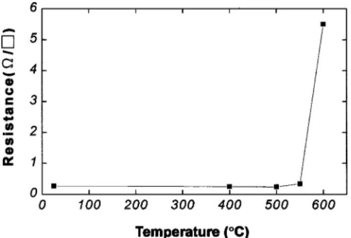
Figure 1 shows the sheet resistances of the samples
as-a兲To whom correspondence should be addressed; electronic mail:
FIG. 1. Sheet resistance of the samples as-deposited and after annealing at various temperatures.
APPLIED PHYSICS LETTERS VOLUME 77, NUMBER 21 20 NOVEMBER 2000
3367
0003-6951/2000/77(21)/3367/3/$17.00 © 2000 American Institute of Physics
This article is copyrighted as indicated in the article. Reuse of AIP content is subject to the terms at: http://scitation.aip.org/termsconditions. Downloaded to IP: 140.113.38.11 On: Thu, 01 May 2014 07:38:54
deposited and after 400–600 °C annealing. The sheet resis-tance of the TaNx/Cu/Ta/GaAs film structure initially drops a little after 400 and 500 °C annealing, which is apparently caused by grain growth and a decrease in defect density in the Cu and Ta films. The sheet resistance increased slightly upon annealing at 550 °C, which implies diffusion and/or reaction occurred. After 600 °C annealing, the sheet resis-tance drastically increased, suggesting that a significant dif-fusion and reaction had occurred between the layers. Figure 2 shows the XRD results. From the XRD data, it is clear that the peaks of Ta and Cu remain unchanged after 500 °C an-nealing, suggesting that Cu/Ta/GaAs interface is still quite stable up to 500 °C. After 550 °C annealing, it is found that the additional peaks can be identified as TaAs2. Formation of
TaAs2 implies that reactions between the substrate and the
Ta layer can take place at 550 °C. This is consistent with the increase of sheet resistance at 550 °C. After 600 °C anneal-ing, the peaks of Cu and Ta disappeared, instead peaks iden-tified to be phases of TaAs and Cu3Ga 共hexagonal structure with lattice parameters of a⫽0.2600 and c⫽0.4229 nm)9are seen, indicating that a significant diffusion and reaction had occurred among the layers. The TaAs2phase is still present
with the peak intensity decreased. The decomposition of TaAs2into As and TaAs below 750 °C has been previously
reported by Saini.10 This result explains the drastically in-creased sheet resistance after 600 °C annealing. Additional evidence showing the stability to 500 °C has been obtained from AES depth profiles in Fig. 3. As can be seen from this figure, the distribution of the elements in the deposited films remain almost unchanged after 500 °C annealing. Figure 4 shows cross-sectional TEM micrographs of the TaNx/Cu/Ta/GaAs structure. In Fig. 4共a兲, it shows that grain growth of the Cu and Ta occurred after 500 °C annealing, and there is no evidence of intermixing of Cu and the Ta barrier layer with the GaAs substrate. The microstructure of the sample annealed at 600 °C is shown in Fig. 4共b兲. The regions in dark contrast are identified as TaAs, and those in FIG. 3. Auger depth profiles of the samples共a兲 as-deposited and 共b兲 after
500 °C annealing.
FIG. 4. Cross-sectional TEM micrographs 共a兲 after 500 °C annealing, 共b兲 after 600 °C annealing,共c兲 TaAs electron diffraction pattern, and 共d兲 Cu3Ga
electron diffraction pattern. FIG. 2. XRD patterns of the samples as-deposited and after annealing at
various temperatures.
3368 Appl. Phys. Lett., Vol. 77, No. 21, 20 November 2000 Chenet al.
This article is copyrighted as indicated in the article. Reuse of AIP content is subject to the terms at: http://scitation.aip.org/termsconditions. Downloaded to IP: 140.113.38.11 On: Thu, 01 May 2014 07:38:54
white are Cu3Ga by selected area electron diffraction pattern
关Figs. 4共c兲 and 4共b兲兴 and x-ray energy dispersive
spectros-copy共EDS兲. The observation of Cu3Ga as a large grain in the
substrate and small grains close to the surface clearly dem-onstrates the severe diffusion of Cu and Ga at high tempera-ture. The chemical analysis of EDS shows that the Cu3Ga
phase also contains a few percent of As. We are not able to identify the location of TaAs2as their size is too small to be
seen in the scale of the image. However, it is speculated that they might locate at the Ta/GaAs interface. From the above results, it is suggested that Cu migration into GaAs substrate with Ta/GaAs interfacial reaction results in failure of the barrier at 600 °C.
Copper metallization on GaAs with Ta as the diffusion barrier layer has been shown to be able to be stable up to 500 °C. After 550 °C annealing, however, the interfacial mix-ing of Ta with GaAs substrate occurred, resultmix-ing in the for-mation of TaAs2 phase, whereas the released Ga may be
dissolved in Cu as the Ga solubility in Cu can be up to 22.2% according to Cu–Ga phase diagram.11 After 600 °C annealing, Ta strongly reacted with GaAs to form TaAs, while Cu penetrated into GaAs to form Cu3Ga. Also, TaAs2
may gradually decompose to TaAs as TaAs could be more stable than TaAs2at high temperature. The surplus As might
then go into Cu3Ga. While further work is necessary to
ex-amine the details of the interdiffusion and reactions of the layers, the stability up to 500 °C should be good enough for the later stages of GaAs device processes. To verify the
ef-fectiveness of Cu metallization, we have applied the Cu/Ta layers to the backside metallization on GaAs MESFETs, it shows comparable performance with conventional Au/Ti layers.12 It is believed that Cu can also be successfully ap-plied to the frontside GaAs devices metallization with the proper modification of the current processes.
The work was sponsored jointly by the Ministry of Edu-cation and the National Science Council, Republic of China, under Contract No. 89-E-FA06-2-4. The authors would like to thank Professor Fu-Rong Chen and Professor Ji-Jung Kai of National Tsing Hua University for their help on TEM observations.
1K. Holloway and P. M. Fryer, Appl. Phys. Lett. 57, 1736共1990兲. 2K. Holloway, P. M. Fryer, C. Cabral, Jr., J. M. E. Harper, P. J. Bailey, and
K. H. Kelleher, J. Appl. Phys. 71, 5433共1992兲.
3D. S. Yoon, H. K. Baik, and S. M. Lee, J. Appl. Phys. 83, 8074共1998兲. 4E. R. Weber, Appl. Phys. A: Solids Surf. 30, 1共1983兲.
5A. Cros, M. O. Aboelfotoh, and K. N. Tu, J. Appl. Phys. 67, 3328共1990兲. 6C. A. Chang, J. Appl. Phys. 67, 566共1990兲.
7
P. H. Wohlbier, Diffusion and Defect Data共Trans Tech, OH, 1975兲, Vol. 10, pp. 89–91.
8C. Kittel, Introduction to Solid State Physics, 7th ed.共Wiley, New York,
1996兲, pp. 126 and 160.
9
D. A. Mirzayev, V. M. Schastilivtsev, S. Y. E. Karzunov, T. R. Shron, and V. G. Ulynov, Phys. Met. Metallogr. 59, 138共1985兲.
10G. S. Saini, L. D. Calvert, and J. B. Taylor, Can. J. Chem. 42, 630共1964兲. 11T. B. Massalski and J. L. Murray, Binary Alloy Phase Diagrams
共Ameri-can Society for Metals, Metals, Park, OH, 1986兲, p. 1411.
12
C. Y. Chen, E. Y. Chang, L. Chang, and S. H. Chen, Electron. Lett. 36, 1317共2000兲.
3369
Appl. Phys. Lett., Vol. 77, No. 21, 20 November 2000 Chenet al.
This article is copyrighted as indicated in the article. Reuse of AIP content is subject to the terms at: http://scitation.aip.org/termsconditions. Downloaded to IP: 140.113.38.11 On: Thu, 01 May 2014 07:38:54