低溫高介電係數材料於有機薄膜電晶體製程之研究
80
0
0
全文
(2) 低溫高介電係數材料於有機薄膜電晶體製程之研究 Study of Organic Thin Film Transistor with High-k Material by Using Low-temperature Supercritical Technology. 研 究 生:周誼明. Student:Yi-Ming Chou. 指導教授:劉柏村. Advisor:Po-Tsun Liu. 國 立 交 通 大 學 電機學院光電顯示科技產業研發碩士班 碩 士 論 文. A Thesis Submitted to College of Electrical and Computer Engineering National Chiao Tung University in partial Fulfillment of the Requirements for the Degree of Master In. Industrial Technology R & D Master Program on Photonics and Display Technologies January 2008 Hsinchu, Taiwan, Republic of Chin. 中華民國九十七年一月.
(3) 低溫高介電係數材料於有機薄膜電晶體製程之研究. 研究生:周誼明. 指導教授:劉柏村. 國立交通大學電機學院產業研發碩士班 摘. 要. 在此論文裡,我們研究了高介電常數材料與薄膜電晶體在超臨界二氧化碳流 體混合水的熱處理下其電性的改變並將此高介電常數薄膜為絕緣層製造有機薄膜 電晶體。首先,在室溫下,利用真空濺鍍系統成長極薄的氧化鉿薄膜,厚度約為 7 奈米,為了取代傳統的高溫退火製程,我們使用了溫度約 150°C 超臨界流體混 合水的技術,為了驗證超臨界流體混合水能有效的使水分子進入到氧化鉿,進而 減少薄膜的缺陷密度,我們經由紅外線光譜儀、熱脫附常壓游離質譜儀與 X 射線 光電子能譜來做材料分析,結果均顯示於氧化鉿薄膜內氧的含量增加,而厚度為 7 奈米氧化鉿薄膜在閘極電壓 3 伏特的操作下,其單位面積漏電流約為 2×10⁻⁷ A/cm2,並且得到較高的崩潰電壓,崩潰電壓約為 24 伏特,傳導機制亦由原本未 經過處理的量子穿隧效應轉換為熱放射效應,以上主要的原因是由於氧化鉿薄膜 的缺陷密度減少。 此外,我們利用經處理過的氧化鉿薄膜為絕緣層去製作有機薄膜電晶體,發 現經由超臨界流體技術的處理之後,有機薄膜電晶體有較好的元件特性,其有機 薄膜電晶體中的臨界電壓、場效移動率、次臨界擺幅和開關電流比例都有顯著的 提升。這些改善主要是因為超臨界流體的技術,能有效修補懸鍵,進而減少氧化 鉿絕緣層的缺陷密度。 由這些結果均顯示,藉由超臨界流體混合水的技術,能減少薄膜的缺陷密度。 可預期的,若超臨界流體的特殊特性整合在高介電常數材料與有機薄膜電晶體, 將具有其優勢。. i.
(4) Study of Organic Thin Film Transistor with High-k Material by Using Low-temperature Supercritical Technology Student:Yi-Ming Chou. Advisor:Dr. Po-Tsun Liu. Industrial Technology R & D Master Program of Electrical and Computer Engineering College National Chiao Tung University ABSTRACT In this study, supercritical fluids (SCF) technology is employed originally to effectively improve the properties of low-temperature-deposited metal oxide dielectric films and fabricate organic silicon thin film transistors (OTFTs). In this work, 7 nm ultra-thin Hafnium Oxide (HfO2) films are fabricated by sputtering method at room temperature, and replacing the conventional high temperature annealing with supercritical fluids treatment at 150 °C. The supercritical fluids act a transporter to deliver H2O molecule into the HfO2 films for repairing defect states. After this proposed process, the absorption peaks of Hf-O-Hf bonding apparently raise and the quantity of oxygen in HfO2 film increases from FTIR and TDS measurement, individually. The leakage current density of 7 nm HfO2 film is cut down to 2×10⁻⁷ A/cm2 at |Vg| = 3 V, and the conduction mechanism is transferred from quantum tunneling to thermal emission because of the significantly reducing the defects in the HfO2 film. Moreover, the higher breakdown voltage is obtained, reaching |Vg| = 24 V. Additionally, supercritical fluids technology is also proposed to effectively passivate the defect states in HfO2 insulator of OTFTs at low temperature (150 °C). After the treatment of supercritical fluids mixed with water and propyl-alcohol, the characteristics of OTFTs are better. This proposed technology is also used to improve the transfer characteristics of OTFTs at 150 °C. From theses experimental results, the better sub-threshold swing, lower off-current, higher on/off current ratio and higher mobility are obtained, such that the supercritical CO2 treatment provide a novel method to enhance the transfer characteristics of Organic thin film transistors. ii.
(5) 誌 謝 首先由衷地感謝指導老師劉柏村博士在我進修碩士學位期間的的指導、教誨 和鼓勵,老師孜孜不倦的研究精神,使我獲益匪淺,不僅僅是在學術研究上的指 導,對於人生規劃及待人處事的態度上,亦讓我獲益良多,僅在此獻上最誠摯的 謝意。諸位口試委員的指導和建議,也在此謹申謝意。 此外,要感謝蔡志宗學長與楊柏宇學長悉心的教導使我得以一窺超臨界流體 領域的深奧,尤其是蔡志宗學長在實驗、量測分析以及論文寫作給予我莫大的協 助與建議,使我在這些年中獲益匪淺,順利獲得知識並取得學位。另外亦得特別 感謝李逸哲學長、李昇翰學長、鄒一德學長、林俊文學長、李啟銘學長、葉唐豪學 長、李崇維學長與鄭逸立學弟的大力協助,因為有你們的陪伴、幫忙及搞笑讓兩 年的研究生活變得多彩多姿。還有要感謝黃震鑠學長、吳興華學長、陳弘根學長、 黃千睿學長、曾子怡學姐、陳又菁學姐、蕭秀娟學姐、鍾宛芳學姐、聶建名學長、 卓立苹學姐,感謝學長姐們平日對我的照顧以及研究上的建議。也要感謝實驗室 一起工作的同學-高逸侑,以及學弟-鄭逸立、竹立煒、郭豫杰、張繼聖、蔡尚 祐、陳思維、林威廷、陳巍方、王超駿、蘇智昱、鄧立峯、楊維哲、黃羿霖…等, 感謝你們陪伴我共同走過這一段甜美的日子,讓我無論是在實驗中或是讀書時永 遠充滿歡樂。還有要感謝我的好友-胡智勇、許顯斌與潘俊六,感謝你們在我求 學的路上一路相挺。同時,衷心感謝國家奈米元件實驗室(NDL)和交大半導體中心 提供良好的研究設備與充分的資源。相當慶幸自己在研究期間有如此多的貴人相 助,要感謝的人太多太多,無法一一列出,謹奉上最真心的感激與祝福。 最後,我願將這份榮耀呈獻給我深愛最後,我願將這份榮耀呈獻給我深愛的 父母親-周豐年先生、盧娟娜女士。感謝父母親多年來辛苦的教導與栽培,一直 在背後默默地支持與關懷我,陪我度過了許多風雨與榮耀的時光,讓我能無後顧 之憂,全力衝刺學業,終於不負所望完成學業,在此獻上我內心最深的謝意。此 外,特別要感謝陪伴我多年的女友-許嘉倩,在背後的默默支持更是我前進的動 力,碩士班兩年因為妳的支持及協助,使我能順利的完成碩士學位,在此由衷的 對妳說聲謝謝。 周誼明 2008年1月. iii.
(6) Contents Chinese Abstract. ………………………………………………………………………………. i. English Abstract. ……………………………………………………………………………. ii. ……………………………………………………………. iii. …………………………………………………………………………………………. iv. Chinese Acknowledgment Contents. Table Captions Figure Captions Chapter 1. ……………………………………………………………………………. vi. …………………………………………………………………………. vii. Introduction. 1.1 Introduction of Organic Thin-Film Transistors (OTFTs) …………………………1 1.2 Metal Oxide dielectric films (High dielectric constant material, High-k) ……2 1.3 Supercritical Fluid Technology ………………………………………………………2 1.4 Motivation…………………………………………………………………………………3. Chapter 2. Experiment Procedures and Principle. 2.1 Fabrication of Metal-Insulator-Silicon (MIS) and Experiment Process………5 2.2 Fabrication of (OTFTs) and Experiment Process……………………………………6 2.3 Properties of Organic Thin Film Transistors 2.3.1 Characteristics of the organic materials……………………………………7 2.3.2 Operation of OTFTs ……………………………………………………………9 2.3.3 Transportation Mechanisms …………………………………………………11 2.3.4 Parameters extraction …………………………………………………………13. iv.
(7) Chapter 3. Analysis and Result. 3.1 Thin Film Analysis of Electrical Characteristics and Discussion 3.1.1 The current density-electric field (J-E) characteristics ………………15 3.1.2 Conduction Mechanism………………………………………………………15 3.1.3 The capacitance-voltage (C-V) characteristics……………………………20 3.1.4 Breakdown voltage measurement and gate bias stress…………………22 3.2 Thin Film Analysis of Material and Discussion 3.2.1 Fourier Trans-form Infrared Spectroscopy (FTIR) Analysis…………24 3.2.2 Thermal Desorption System – Atmospheric Pressure Ionization Mass Spectrometer (TDS-APIMS) Analysis……………………………………25 3.2.3 X-ray Photoelectron Spectroscopy (XPS) Analysis……………………25 3.2.4 Transmission Electron Microscopy (TEM) Analysis……………………26 3.3 OTFTs Analysis of Electrical Characteristics and Discussion 3.3.1 The current density-electric field (J-E) characteristics…………………27 3.3.2 The capacitance-voltage (C-V) characteristics……………………………28 3.3.3 Secondary Ions Mass Spectrometer (SIMS) Analysis…………………29 3.3.4 The current-voltage (I-V) characteristics…………………………………30 3.3.5 The DC bias and current stress characteristics……………………………31 3.4 Summary……………………………………………………………………………………32. Chapter 4. Conclusion. References. ………………………………………………………………………………………63. ……………………………………………………………………34. v.
(8) Table Captions Chapter 1 Table 1-1. Critical temperature and pressure for some common fluids……………… 36. Table 1-2. Comparison of physical properties of CO2…………………………………… 36. Chapter 2 Table 3-1. The extracted parameters from C-V curves of HfO2 films after different treatment, measuring at 1M Hz with gate bias swing from negative voltage to positive voltage (forward). The Vfb means the flat-band voltage, and defined as C/Cmax = 50%. The change of flat-band voltage of different- treated HfO 2 films under forward swing is label as ΔV. ………………………………………………………………………………… 62. vi.
(9) Figure Captions Chapter 1 Fig. 1-1. Phase diagram for CO2…………………………………………………………… 35. Fig. 1-2. Density-pressure-temperature surface for pure CO2. …………………… 35. Chapter 2 Fig. 2-1. The supercritical fluid system. ………………………………………………… 37. Fig. 2-2. The experiment processes of thin HfO2 film with various treatments.… 38. Fig. 2-3. The experiment processes of OTFTs with HfO 2 film of various Treatments. ………………………………………………………………………… 39. Fig. 2-4. The energy band diagram of entacene. The optical energy gap and adiabatic energy gap are determined.. Fig. 2-5. Energy band diagrams. (a). ……………………………………… 40. for a p-channel (pentacene) and. (b). for a. n-channel (NTCDA) OTFT. The left side shows the devices at zero gate bias, while in the centre and in the right parts the accumulation and depletion mode operation regimes are presented. ………………………… 40 Chapter3 Fig. 3-1. The leakage current densities of HfO2 films after different treatments (The negative bias is applied on gate electrode). ………………………… 41. Fig. 3-2. Conduction mechanism for Al/HfO2/Si MIS structure. ………………… 41. Fig. 3-3. (a). Curve of ln. (J/E). versus reciprocal of electric field. (1/E) for the. baking-only treated HfO2 film, and a schematic energy band diagram accounting for trap-assisted tunneling shown in the inset. (b) Leakage current density versus the square root of electric field (E1/2) plot for the. vii.
(10) 3000 psi-SCCO2 treated HfO2 film. The inset shows the energy band diagram of Schottky-type conduction mechanism. ……………………… 42 Fig. 3-4. The leakage current densities of HfO2 films after different treatments (The positive bias is applied on gate electrode). …………………………… 43. Fig. 3-5. The capacitance-voltage characteristics of HfO2 films after different treatment, measuring at 1M Hz with gate bias swing from negative voltage to positive voltage (forward) and from positive voltage to negative voltage (reverse). …………………………………………………………………………… 43. Fig. 3-6. The mechanism of extracting of fixed charge with SCCO2 fluids. …… 44. Fig. 3-7. The equivalent capacitance models of MOS structure (a) without Cit, (b) with Cit.. Fig. 3-8. …………………………………………………………………………… 45. The capacitance-voltage characteristics of HfO2 films after different treatment, measuring at 1M Hz and 100k Hz with forward gate bias swing. ……………………………………………………………………………… 45. Fig. 3-9. The breakdown characteristic curves of HfO 2 films after various treatments (a) at positive and (b) at negative gate bias region, individually.. Fig. 3-10. ……………………………………………………………………… 46. The variation of leakage current of different-treated HfO2 films as a function of stress time at a high electric field = 5 MV/cm. ……………… 47. Fig. 3-11. The FTIR spectra of HfO2 films after various post-treatments, including Baking-only, H2O vapor and 3000psi-SCCO2 treatment. ……………… 47. Fig. 3-12. The transporting mechanism for SCCO2 fluids taking H2O molecule into HfO2 film. ………………………………………………………………………… 48. viii.
(11) Fig. 3-13. The thermal desorption spectroscopy (TDS). measurement,. (a). m/e. (mass-to-charge ratio) = 32 peak that is attributed to O2, (b) m/e = 18 peak that is attributed to CO2 . ………………………………………………… 49 Fig. 3-14. The X-ray photoemission spectra of HfO2 films O 1s after various post-treatments, including (a) Baking-only, (b) H2 O vapor and (c) 3000psi-SCCO2 treatment. …………………………………………………… 50. Fig. 3-15. The TEM images show the MIS (Al/HfO2/Si-Substrate) structure after various post-treatments: (a) Baking-only treatment (b) H2 O vapor treatment and (c) 3000psi-SCCO2 treatment. ……………………………… 51. Fig. 3-16. The leakage current densities of HfO2 films after different treatments. ………………………………………………………………………………………… 52. Fig. 3-17. The capacitance-voltage characteristics of HfO2 films after different treatment, measuring at 1M Hz with gate bias swing from negative voltage to positive voltage (forward) and from positive voltage to negative voltage (reverse). …………………………………………………………………………… 52. Fig. 3-17. Secondary ion mass spectroscopy: (a) Si atom (b) Hf atom and (c) O atom in HfO2 film of Baking-only and 3000 psi-SCCO2 treatment ………… 53. Fig. 3-18. Current vs Voltage plots (ID-VG) characteristics of HfO2 film: (a) Baking-only treatment and (b) H2O vapor treatment. (OTFTs deposited on HfO2 film with 3000 psi-SCCO2 treatment). ………………………… 54. Fig. 3-19. Current vs Voltage plots (ID-VG) characteristics: (a) HfO2 film of 3000 psi-SCCO2 treatment and (b) PECVD SiO2 film. ………………………… 55. Fig. 3-20. Current vs Voltage plots (ID-VD) characteristics: (a) HfO2 film with 3000 psi-SCCO2 treatment and (b) PECVD SiO2 film. ………………………… 56. Fig. 3-21. Normailzed Current vs Voltage plots (ID-VD) characteristics of HfO2 film ix.
(12) with 3000 psi-SCCO2 treatment and PECVD SiO2 film. Fig. 3-22. ……………… 57. Current vs Voltage (IG-VD) characteristics of a OTFTs deposited on HfO2 film with 3000 psi-SCCO2 treatment : (a) DC bias stress of VG= -20V, (b) DC bias stress of VG= -20V and VD= -20V and (c) DC bias stress of VG= -20V and current stress of VD= -200nA. …………………………………… 58. Fig. 3-23. Mobility shift vs. bias stress time for DC bias stress of VG= -20V, DC bias stress of VG= -20V and VD= -20V and DC bias stress of VG= -20V and current stress of VD= -200nA (OTFTs deposited on HfO2 film with 3000 psi-SCCO 2 treatment). …………………………………………………… 59. Fig. 3-24. Threshold voltage shift vs. bias stress time for DC bias stress of VG= -20V, DC bias stress of VG= -20V and VD= -20V and DC bias stress of VG= -20V and current stress of VD= -200nA (OTFTs deposited on HfO2 film with 3000 psi-SCCO 2 treatment). …………………………………… 59. Fig. 3-25. Current vs Voltage (IG-VD) characteristics of a OTFTs deposited on PECVD SiO2 film : (a) DC bias stress of VG= -20V, (b) DC bias stress of VG= -20V and VD= -20V and (c) DC bias stress of VG= -20V and current stress of VD=-200nA. ………………………………………………………… 60. Fig. 3-26. Mobility shift vs. bias stress time for DC bias stress of VG= -20V, DC bias stress of VG= -20V and VD= -20V and DC bias stress of VG= -20V and current stress of VD= -200nA (OTFTs deposited on PECVD SiO2 film) ………………………………………………………………………………… 61. Fig. 3-27. Threshold voltage shift vs. bias stress time for DC bias stress of VG= -20V, DC bias stress of VG= -20V and VD= -20V and DC bias stress of VG= -20V and current stress of VD= -200nA (OTFTs deposited on PECVD SiO2 film).………………………………………………………………………… 61. x.
(13) Chapter 1 Introduction 1.1. Introduction of Organic Thin-Film Transistors (OTFTs) The concept of using organic materials as semiconductors layer in transistors are. realized at least since the 1980s [1,2]. Latterly, the organic thin film transistors (OTFTs) are of interest for the fabrication of low-cost, simple process and flexible displays. The OTFTs performance has been improved in the past decade and comparable to the hydrogenated amorphous silicon transistors (a-Si:H TFT) [3]. To fabricate organic transistors on plastic substrate, it is essential to decrease the process temperature. Many researchers have proposed individual methods to fabricate the pentacene-transistors and the reported field-effect mobilities are in the range of 0.001 ~ 3cm2/V-sec [4]. However, the OTFTs still face several problems: low-temperature gate dielectrics, reliably simple processes and low-mobility etc. At these issues, a more convenient for gate dielectric must be surmount a major obstacle. Lately, the high-capacitance gate dielectrics can be achieved by the two methods. One is reducing the gate-dielectric thickness [5], the other was using the high-k material as the gate-dielectrics [6]. In low temperature deposited process, the high-k materials may low dielectric strength and ascend high leakage current in the utilization of OTFTs. The pinhole may be another question when reducing the dielectric thickness. So, a new dielectric is provided with higher dielectric permittivity, controllable insulator thickness and to reduce leakage current. That will be improving the OTFTs.. 1.
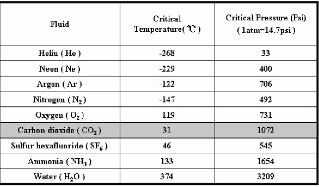
(14) 1.2 Metal Oxide dielectric films (High dielectric constant material, High-k) The Majority of metal oxide dielectric films, such as HfO2, Ta2O5 and Al2O3, hold higher dielectric constant than thermal oxide(SiO2), and studied to replace the gate dielectric layer for future generation CMOS devices because of the lower leakage current and thicker physics thickness than thermal oxide (SiO2) under identical equivalent oxide thicknesses (EOT) [7, 8]. Additionally, due to the property of high dielectric constant, For thin film transistors, in pervious records, the use of low-temperature-deposited metal oxide films as gate dielectrics not only reduces the threshold voltage to near zero for pentacene and zinc oxide (ZnO2) TFTs but also the thickness of the gate insulator to nanometer scale [9, 10]. For extending the application, the novel method to improve the quality of metal oxide films is necessary.. 1.3. Supercritical Fluid Technology Supercritical fluids technology is a novel low temperature trap-passivation. technology. The technology is compounds above their critical temperatures and pressure, as shown in Fig 1-1 [11, 12]. The advantage of supercritical fluids for commercial applications is their unique combination of liquid-like and gas-like properties. The Table 1-1 shows critical temperature and pressure for some common fluids. CO2-based supercritical fluids are particularly attractive because CO2 is nontoxic, nonflammable, obtain easily and lower price. Besides, its critical conditions are easily achievable with existing process equipment (31 °C, 1072 psi =72.8 atm). Figure 1-2 shows the density-pressure-temperature surface for pure CO2. It can be discovered that relatively small changes in temperature or pressure near the critical. 2.
(15) point, resulting in large changes in density. Table 1-2 shows the comparison of several physical properties of typical liquid, vapor, and supercritical fluid state for CO2. It could be seen that supercritical CO2 (SCCO2) fluids possesses liquid-like density, so that SCCO2 fluids are analogous with light hydrocarbon to dissolve most solutes and own exceptional transport capability [13, 14]. Besides, SCCO2 fluids hold gas-like characteristic due to their viscosity and surface tension are extremely low, it allows SCCO2 fluids to keep fine diffusion capability and enter the nano-scale pores or spaces without damage. These properties are the reasons for SCCO2 fluids to employ in many commercial applications, including the extraction of caffeine from coffee, fats from foods, and essential oils from plants for using in perfumes. Furthermore, in last years, many records are investigated with SCCO2 fluids to apply in semiconductor fabrication, such as cleaning wafer and stripping photoresist, by means of its high mass transfer rates and infiltration capabilities [14-16].. 1.4 Motivation In recent records, Metal oxide dielectrics, such as HfO2, Ta2O5, and Al2O3 have attracted much attention for memory cell capacitors and gate dielectric applications in the ultra large scale integration (ULSI) technology [7, 8]. Among several metal oxide film formation methods [7, 8, 17], in general, low-temperature technology is welcome due to a low thermal and low price process. Also, it is suitable for thin film transistor liquid crystal displays (TFT-LCDs) technology on the base of glass substrates or plastics. However, the low-temperature-deposited dielectric films perform inferior properties and larger current leakage due to numerous traps inside the metal oxide film [18, 19]. Hence, the low-temperature-deposited metal oxide film to reduce electrical traps by implementing a post-treatment process is needed. The supercritical. 3.
(16) fluids technology has been applied to remove photoresist and impurity in integrated circuit (IC) fabrications [20]. It is also operative method to extract moisture from structures of nanoscale, such as porous dielectric-material and carbon nano-tube [21, 22]. By the liquid-like property, it is allowed for supercritical fluids to own fine transport capability [23]. Supercritical fluids, in addition, hold gas-like and high-pressure properties to efficiently diffuse into thin films with no damage. Here, these advantages would be adequately employed to passivate the defects in lowtemperature-deposited metal oxide dielectric film at 150 °C. In addition, OTFTs will extensively research in the flexible displays. The excellent transfer characteristics are thereby demanded, such as high mobility and lower threshold voltage. Especially, in recent years, the fabrication of OTFTs tends to being implemented at low temperature processes for cost down and comparable with plastic substrates (120~250 °C)[24, 25]. The performance of low-temperature process for OTFTs, however, due to the poor gate dielectrics with great quantity of defects is unsuitable for application to display technology, [26]. For improving electrical characteristics of OTFTs, it is necessary to passivate the defect-states in the gate dielectrics. Therefore, it is critical to develop a low-temperature traps passivation technology for extending the application of OTFTs. In this work, therefore, the supercritical fluids treatment is also proposed to effectively decrease the defects in the gate dielectrics of OTFTs at low temperature.. 4.
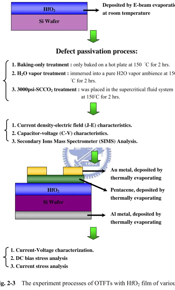
(17) Chapter 2 Experiment Procedures and Principle 2.1. Fabrication of Metal-Insulator-Silicon and Experiment Process At first experiment, a metal-oxide HfO2 film layer was deposited on p-type (100). silicon wafers by reactive DC magnetron sputtering at room temperature under Ar/O2 ambient. The thickness of as-deposited HfO2 films was 7nm, which was measured by an ellipsometer system. Subsequently, the wafers with 7nm-thick HfO2 film were split into three groups, and processed with different post-treatments to study the properties of low-temperature-deposited HfO2 film. The first group labeled as Baking-only treatment, was designed as the control sample, and was only baked on a hot plate at 150 °C for 2 hrs. The second group labeled as H2O vapor treatment, was immersed into a pure H2O vapor ambience at 150 °C for 2 hrs in a pressure-proof stainless steel chamber with a volume of 100cm3. The third sample marked as 3000psi-SCCO2 treatment, was placed in the supercritical fluid system at 150°C for 2 hrs, where was injected with 3000psi of SCCO2 fluids mixed with 5 vol.% of propyl alcohol and 5 vol.% of pure H2O. The propyl alcohol plays a role of surfactant between nopolar-SCCO2 fluids and polar-H2O molecules, so that the H2O molecule uniformly distributes in SCCO2 fluids and be delivered into the HfO2 film for passivating defects. The supercritical fluid system is shown in Fig. 2-1. After these different treatments, the thickness of HfO2 films is almost intact, checked with the ellipsometer measurement. Fourier transformation infrared spectroscopy (FTIR) and thermal desorption spectroscopy (TDS) were also used to investigate the evolution of chemical functional bonding and the content of oxygen in HfO2 films, respectively. Electrical measurements were conducted on metal insulator. 5.
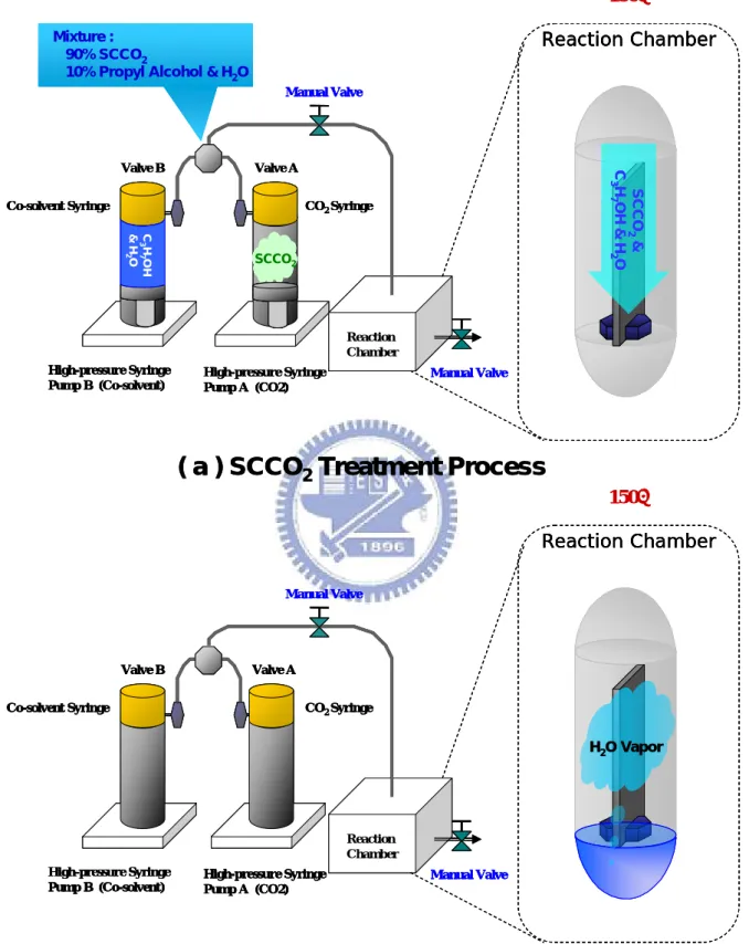
(18) semiconductor (MIS) capacitors by thermally evaporating Al electrodes on the front surface of the HfO2 films and the backside of the silicon wafer. The current density-electric field (J-E) characteristics, capacitance-voltage (C-V) characteristics, breakdown voltage and gate bias stress were measured with HP4156C semiconductor parameter analyzer for investigating the transformation of HfO2 film. The experiment processes of thin HfO2 film with various treatments are exhibited in Fig. 2-2.. 2.2. Fabrication of OTFTs and Experiment Process At second experiment, a metal-oxide HfO2 film layer was deposited on p-type. (100) silicon wafers by E-beam thermally evaporating at room temperature. The thickness of as-deposited HfO2 films was 150nm, which was measured by an ellipsometer system. Subsequently, the wafers with 150nm-thick HfO2 film were split into three groups, and processed with different post-treatments to study the properties of low-temperature-deposited HfO2 film. The first group labeled as Baking-only treatment, was designed as the control sample, and was only baked on a hot plate at 150 °C for 2 hrs. The second group labeled as H2O vapor treatment, was immersed into a pure H2O vapor ambience at 150 °C for 2 hrs in a pressure-proof stainless steel chamber with a volume of 100cm3. The third sample marked as 3000psi-SCCO2 treatment, was placed in the supercritical fluid system at 150°C for 2 hrs, where was injected with 3000psi of SCCO2 fluids mixed with 5 vol.% of propyl alcohol and 5 vol.% of pure H2 O. The propyl alcohol plays a role of surfactant between nopolar-SCCO2 fluids and polar-H2O molecules, so that the H2O molecule uniformly distributes in SCCO2 fluids and be delivered into the HfO2 film for passivating defects. After these different treatments, The gate contact by thermally evaporating Al. 6.
(19) electrodes on the backside surface of the silicon wafer. Then, the wafer was put into the oven with HMDS steam for 20mins at 150 degree. Pentacene was used as an active layer. This was deposited using ULVAC thermal evaporator. The deposition is started at a pressure lower than 3×10⁻⁶ torr. The deposition rate is controlled at 0.1Å/s. The temperature we use in depositing pentacene films is 70℃. We use shadow mask to define the active region of each device. the resulting thickness of the pentacene thin film was 70 nm, which was measured by a quartz-crystal thin film thickness monitor. After pentacene deposition, We use shadow mask to define top contact of each device. The top electrodes are Au. We deposited the Au (100nm) via the thermal evaporator as the source and drain electrode pad. The deposition pressure was at 3×10⁻⁶ torr with the deposition rate of 0.5Å/sec. In addition, we fabrication the same process to comparison with insulation of SiO2 by Plasma Enhanced Chemical Vapor Deposition (PECVD). After fabrication OTFTs, The current density-electric field (J-E) characteristics, capacitance-voltage (C-V) characteristics, Current-Voltage (I-V) characteristics, current stress and DC bias stress were measured with HP4156C semiconductor parameter analyzer for investigating the OTFTs. The experiment processes of OTFTs with various treatments are exhibited in Fig. 2-3.. 2.3. Properties of Organic Thin Film Transistors. 2.3.1 Characteristics of the organic materials Organic conjugated materials can be generally sorted small molecules and polymers in OTFTs. The one single bond exhibit contiguous sequences of double bonds separated. The π orbital in the conjugated system is linked with the neighboring π orbital, and spreads in the whole molecule. The π electrons are delocalized across. 7.
(20) the molecule, which makes conductive or semiconducting characteristics of the conjugated system. Unlike the case in inorganic semiconductors, the carrier transport is band-like transport which is determined by the Bloch wave states. Carrier transport is via hopping between localized states in disordered organic semiconductors. Mobility is the most important parameter when we mention about OTFTs. The localized wave functions in organic semiconductors lead to small inter-molecular interactions, typically the weak π-π overlap or van der Waals. That is the main cause of the low mobility. But it can be improved by modifying the materials and device architectures. Pentacene is one of the most widely-used in OTFTs materials. Its mobility has reached the fundamental limit (> 3 cm2/Vs) [27.28] which is obtained with a single crystal at room temperature. Organic semiconductors are soluble in vaporizable or organic solvents at low temperatures due to such small inter-molecular interactions. This implies that there may be a trade-off between the mobility and processability in organic semiconductors of OTFTs. The mobility of organic semiconductors ranged from 0.001 to 3 cm2/Vs is comparable to that of amorphous silicon transistors which is widely developed and used in flexible displays. First introduces the polymer material. Conjugated polymers are more suitable than small molecules for solution processability due to their high viscosity. However, the mobility of conjugated polymer is generally smaller than that of small molecule semiconductors for the more random orientation of molecular units or relatively short conjugated length in polymer backbones. The mobility as high as 0.1cm2/Vs has been achieved with regioregular head-to-tail poly(3-hexylthiophene) [29]. More recently, it has been shown that the mobility can be raised to 0.2cm2/Vs when the polymer film is applied by dip-coating to a thickness of only 2-4nm [30]. Polymer-based TFTs offer the advantage of spin-coating or inkjet printing, but in turn decreases the mobility, the. 8.
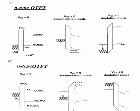
(21) purity defects in material may give rise to charge-trapping sites. In addition, introduces the small molecules material. Since the spin-coated polymer is disordered in structure, the structure of thermal evaporated small molecule is well ordered. Small molecules can be classified into linear fused ring compounds, 2-D fused ring compounds, oligomers, and 3-D molecules. Most organic materials tend to transport holes better than electrons. This is because the OTFTs is p-type semiconductors are more stable in air and larger mobility. Most n-type organic semiconductors are sensitive to moisture and air due to the organic anions. Especially, the carbanions can easily react with water and oxygen under operating conditions, which causes the low mobility of n-type organic semiconductors. Thereupon, we choose pentacene as material of the semiconductor region. Because pentacene material is have the largest mobility and more stability. Pentacene is an aromatic compound with five condensed benzene rings, the chemical formula is C 22 H 14 with molecular weight 278.3. The volume of the unit cell is about 705Å [31]. The permittivity is 4 [32], and the electron affinity is about 2.49eV. Silinish et al. determined the adiabatic energy gap ( E GAd ) by using the threshold function of intrinsic photoconductivity of pentacene [33]. The second transition is from the excited state to the ionic state, which is called the optical energy gap ( E GOpt ).The energy band of pentacene. are exhibited in Fig. 2.4 [34]. 2.3.2 Operation of OTFTs Organic thin-film transistors are basically similar to traditional thin-film transistors in structure. Two common device structures are used in organic TFTs. Although there is not large difference between inorganic TFTs and organic TFTs, the. 9.
(22) operation modes of these two kinds of transistors are not the same at all. Since pentacene is a p-type semiconductor. First, a negative bias is applied to the gate, the voltage drops over the insulator and semiconductor regions, which gives rise to band bending in the semiconductor. The additional positive charges provided by the source and drain electrodes accumulate charges in this region. The insulator serves as a capacitance which stores charges and can be represented as COX. It is assumed that a little voltage drop across the semiconductor is negligible. In this situation, the applied drain bias can direct the current from source to drain. The conduction is determined by mobility μ which represents how the electrical field drives the accumulated charges. Therefore, the increased gate voltage δVG accounts for the increased charges COXδVG and the total charges increased over the channel are WLCOXδVG, where L and W correspond to the channel length and width. The increased drain current δID then represented as. δI D ≈. W C OX μV D δVG L. (2.1). In general, we can divide the operation of OTFTs into two regions, linear and saturation regions. The drain current in the linear region is determined from the following equation. ID =. V W COX μ (VG − VTH − D )VD 2 L. (2.2). Since the drain voltage is quite small, sometimes equation (2.2) can be simplified as ID =. W C OX μ (VG − VTH )V D L. (2.3). For -ID > -(VG - VTH ), ID tends to saturate due to the pinch-off of the accumulation layer. The current equation is modified as. 10.
(23) ID =. W C OX μ (VG − VTH ) 2 2L. (2.4). The energy band diagrams for n-type and p-type OTFTs are shown in Fig. 2.5 [35].. 2.3.3. Transportation Mechanisms. Latterly, two principal types of theoretical model are used to describe the transport in organic semiconductors : “The band-transport model” and “The hopping models”. Multiple trapping and release (MTR) model assumes that most of the carriers injected in the semiconductor are trapped in states localized in the forbidden gap. MTR model is widely used in amorphous silicon TFTs [36.37] and explains reasonably well the observed characteristics in vapor-deposited polycrystalline pentacene films. The model assumes that the intrinsic charge transport mechanism is the one involving extended states, and a distribution of traps exists in the forbidden gap above the valence-band edge. At low gate biases, most of the holes injected in the semiconductor are trapped into these localized states. The deepest traps are first filled and carriers can be thermally released. As the negative gate bias increases in p-type materials, the Fermi level approaches the valence-band edge and more traps are filled. At an appropriately high gate voltage, all trap states are filled and subsequently injected carriers move with the microscopic mobility in the delocalized (valence) band [38.39]. Several trap levels have been reported for polycrystalline vapor-deposited pentacene films at depths ranging from 0.06eV to 0.68eV [40], which can account for the MTR model. Traps are sometimes caused from the impurities and structure defects in the crystalline pentacene film which include dislocations, point defects and most importantly, the grain boundaries [41]. The concept of grain boundaries has been used to explain the gate-voltage dependence of mobility in polycrystalline oligothiophene. 11.
(24) films [42.43]. The energy barrier created in the grain boundaries is a function of trapped charge states, carrier concentration within the grains and temperature. At high temperatures, the charge transport is dominated by the thermionic emission over the potential barrier at grain boundaries. At low temperatures, the carrier transport is dominated by tunneling. However, mobility in molecular crystal is still moderate at very low temperatures. The corresponding mean free path does not exceed the inter-molecular distance, which is not physically acceptable for a diffusion-limited transport. Polaron models have been proposed to rationalize the discrepancy [44]. In spite of the recent efforts, the best explanation and exact phenomenon describing the carrier transport in molecular crystals are still under investigation. The concept of variable range hopping (VRH) [45] is usually used in organic transistors, where the carriers transport by hopping: thermally activated carriers tunneling between localized states including percolation, rather than by the activation of carriers to a transport level. The model describes the conductivity in the polymer as equivalent to transport through a resistor network. The percolation criterion through the network is then related to the temperature, the position of Fermi level, and the width of the exponential tail of the density of states. A carrier may either hop over a long distance with low activation energy or hop over a small distance with high activation energy. As the accumulated charges fill the lower lying states, any additional charges will occupy states with relatively higher energy. Therefore, these additional charges just need less energy to hop away to neighboring sites, and the mobility will rise as the gate voltage increases.. 12.
(25) 2.3.4. Parameters extraction. In this section, we introduce four parameters are used to evaluate the performance of OTFTs. They are field effect mobility, threshold voltage, sub-threshold slope and on/off current ratio. Mobility Field effect carrier mobility is usually considered the most critical part of these four parameters. The behavior of an OTFT is revealed with the observation of carrier mobility. Mobility of an OTFT is affected by many factors, such as the trap density of active layer, ambient temperature, and carrier concentration. In OTFTs, the mobility mainly depends on the ordering of molecules and trap density. Generally, mobility can be extracted from the trans-conductance in gm the linear region : WC O X ⎡ ∂I ⎤ gm = ⎢ D ⎥ = μV D L ⎣ ∂VG ⎦ VD =CONSTANT. (2.5). Mobility can also be extracted from the slope of the curve of the square-root of drain current versus gate voltage in the saturation region, i.e. –VD > –(VG - VTH) :. ID =. W μCOX (VG − VTH ) 2L. (2.6). On/Off current ratio Devices with high on/off current ratio represent ratio of the large turn-on current and small off current. It determines the gray-level switching of the displays. High on/off current ratio means there are enough turn-on current to drive the pixel and sufficiently the low current when the device is turned off. Threshold voltage Threshold voltage is related to the power consumptions and the operation voltage of OTFTs. Many researches on OTFTs are suffered from the large threshold voltage.. 13.
(26) Threshold voltage is influenced by the ratio of the mobile and trapped carriers at the interface between the organic semiconductor layer and insulator. There are also researches on lowering the threshold voltage by adjusting the insulator layer [46]. In our experiments, we extract the threshold voltage from equation (2.6), the intersection point of the square-root of drain current versus gate voltage when the device is in saturation mode operation.. Sub-threshold Slope Sub-threshold voltage is defined to evaluate the sensitivity of drain current to gate voltage in OTFTs. The following equation is used to define sub-threshold voltage. Obviously, a well-performed TFT will have a smaller value of sub-threshold voltage. This means that the relatively large swing of drain current can be achieved with a relatively small gate voltage.. 14.
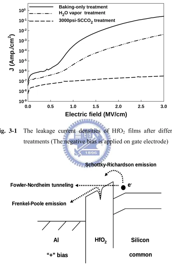
(27) Chapter 3 Analysis and Result 3.1. Thin Film Analysis of Electrical Characteristics and Discussion. 3.1.1. The current density-electric field (J-E) characteristics. The leakage current densities of HfO2 films after different treatments are shown as a function of applied negative gate bias voltage in Fig. 3-1. Among various post-treatments, the baking-treated HfO2 film exhibits the most serious leakage current, inferentially due to its poor dielectric characteristics with numerous traps inside the HfO2 film and the interface between parasitical SiOx and Si wafer. The improvement of electrical characteristics is observed by using H2O vapor process, however, a high leakage current density still appears at larger applied voltages. It could be inferred reasonably dependent on the defect passivation efficiency. The most indicating that H2O vapor can passivate the traps (or defects) and alter dielectric properties of the low-temperature-deposited HfO2 film. After H2O vapor treatment, effective improvement of electrical characteristic is obtained by the 3000 psi-SCCO2 treatment, exhibiting the lowest leakage current density among all samples. Low leakage current density (~2×10⁻⁷ A/cm2) is kept constantly, even biased at an electric field of 3 MV/cm. The electrical performance agrees with FTIR analysis, in which 3000 psi-SCCO2 treatment modified HfO2 dielectrics even effectively.. 3.1.2. Conduction Mechanism. There may be different conduction mechanisms in the insulator thin film, including Schottky-Richardson emission [47], Frenkel-Poole emission [47,48], Fowler-Nordheim tunneling [47,48], and trap assisted tunneling [49,50] illustrated in. 15.
(28) Fig 3-2. The Schottky-Richardson emission generated by the thermionic effect is caused by the electron transport across the potential energy barrier via field-assisted lowering at a metal-insulator interface. The leakage current governed by the Schottky-Richardson emission is as following: 1 J SR = A * T 2 exp⎛⎜ β SR E 2 − φ SR k B T ⎞⎟ ⎝ ⎠. (. where β SR = q 3 4πε 0 ε. ). 1. 2. (3.1). , q is the electronic charge, A* is the effective. Richardson constant, φSR is the contact potential barrier, E is the applied electric field, ε 0 is the permittivity in vacuum, ε is the high frequency relative dielectric constant, T is the absolute temperature, and k B is the Boltzmann constant. We can find the slope of the leakage current equation.. ln J SR = β SR E. 1. 2. [ (. ). k BT + ln A * T 2 − φ SR k BT. Solpe = β SR k B T. ]. (3.2). (3.3). The Frenkel-Poole emission is due to field-enhanced thermal excitation of trapped electrons in the insulator into the conduction band. The leakage current equation is: 1 J FP = J 0 exp⎛⎜ β FP E 2 − φ FP k B T ⎞⎟ ⎝ ⎠. where J 0 = σ 0 E. (. (3.4). is the low-field current density, σ 0 is the low-field. conductivity, β FP = q 3 πε 0ε. ). 1. 2. , q is the electronic charge, φ FP is the contact. potential barrier, E is the applied electric field, ε 0 is the permittivity in vacuum, ε is the high frequency relative dielectric constant, T is the absolute temperature, and. k B is the Boltzmann constant. We can find the slope of the leakage current equation.. 16.
(29) ln J FP = β FP E. 1. 2. k BT + [ln( J 0 ) − φ FP k B T ]. (3.5). Solpe = β FP k B T. (3.6). The Fowler-Nordheim tunneling is the flow of electrons through a triangular potential barrier. Tunneling is a quantum mechanical process similar to throwing a ball against a wall often results that the ball goes through the wall without damaging the wall or the ball. It also loses no energy during the tunnel event. The probability of this event happening, however, is extremely low, but an electron incident on a barrier typically several nm thick has a high probability of transmission. The Fowler-Nordheim tunneling current I FN is given by the expression [51]: I FN = AG AFN ε ox2 exp (− B FN ε ox ). (3.7). where the AG is the gate area, ε ox is the oxide electric field, and AFN and BFN are usually considered to be constant. AFN and BFN are given as the following: AFN = q 3 (m mox ) 8π hΦ B = 1.54 × 10 −6 (m mox ) Φ B. (. BFN = 8π 2moxΦ B3. ). 1. 2. [. 3eh = 6.83 × 10 7 (m mox )Φ B3. ]. 1. 2. (3.8). (3.9). where mox is the effective electron mass in the oxide, m is the free electron mass, q is the electronic charge, and Φ B is the barrier height at the silicon-oxide interface given in units of eV in the expression for BFN . Φ B is actually an effective barrier height that take into account barrier height lowering and quantization of electrons at the semiconductor surface. Rearranging I FN formula gives by:. (. ). (. ). ln I FN AG ε ox2 = ln J FN ε ox2 = ln ( AFN ) − BFN ε ox. 17. (3.10).
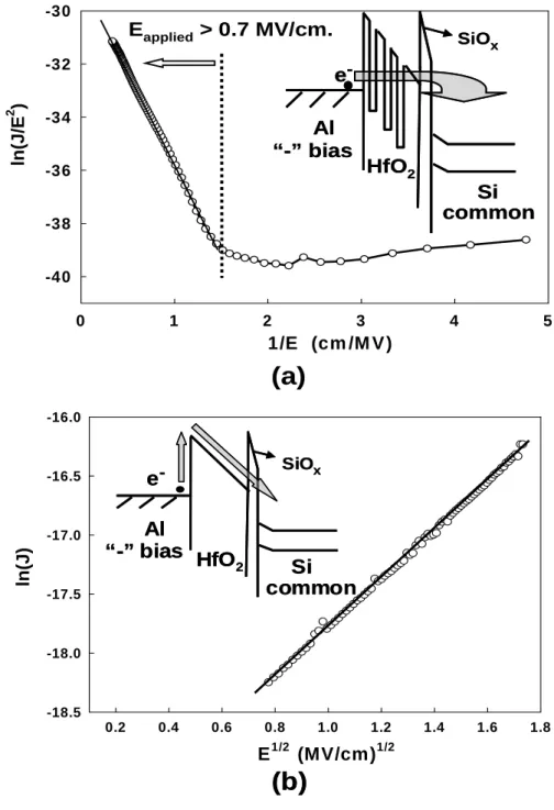
(30) A plot of ln (J FN ε ox2 ) versus (1 ε ox ) should be a straight line if the conduction through the oxide is pure Fowler-Nordheim conduction [51]. In the trap assisted tunneling model, it is assumed that electrons first tunnel through the SiOX interfacial layer (direct-tunneling). Then, electrons tunnel through traps located below the conduction band of the high-k thin film and leak to substrate finally [49]. The equation of leakage current density is [50]: J = α E ox exp(− β E ox ). (3.11). From the equations as shown above, leakage current behaviors of insulate films can be investigated further on the leakage current density J electric field E characteristics such as J vs. E. 1. 2. plots.. The plot of the nature log of leakage current density versus the square root of the applied electric field was observed. It is found that the leakage current density is linearly related to square root of the applied electric field. The linear variations of the current correspond either to Schottky-Richardson emission or to Frenkel-Poole conduction mechanism. For trap states with coulomb potentials, the expression is virtually identical to that of the Schottky-Richardson emission. The barrier height, however, is the depth of the trap potential well, and the quantity β FP is larger than in the case of Schottky-Richardson emission by a factor of 2. Leakage conduction mechanism is also investigated to support the comments on the electrical improvement of HfO2 film. Fig. 3-3(a) plots ln (J/E) versus reciprocal of electric field variation for the baking-only treated HfO2 film, and a schematic energy band diagram accounting for leakage transport mechanism shown in the inset. A good linear fitting explains Fowler-Nordheim (F-N) tunneling [52] occurs in the electric fields higher than 0.7 MV/cm. Also, it is consistent with the electrical behavior of. 18.
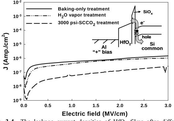
(31) baking-only treated HfO2 film in Fig. 3-1 that leakage current density sharply increases, while gate bias voltage larger than 0.7 MV/cm. This could be attributed to the trap-assisted tunneling due to numerous traps inside the 150°C- baking treated HfO2 film [53]. For the 3000 psi-SCCO2 treated HfO2 film, a plot of leakage current density versus the square root of the applied field (E1/2) gives a good representation of the leakage behavior at high electric fields, as shown in Fig. 3-3(b). The leakage current density of the 3000 psi-SCCO2 treated HfO2 is linearly related to the square root of the applied electric field, demonstrating Schottky-Richardson emission transport mechanism [54]. The Schottky-type conduction can be verified by. (. comparing the theoretical value of β SR = q 3 4πε 0 ε. ). 1. 2. with the calculated one. obtained from the slope of the experimental curve ln J versus E1/2 [55], where q is the electronic charge, ε 0 the dielectric constant of free space, ε is the high frequency relative dielectric constant. The Schottky emission generated by the thermionic effect is caused by electron transport across the potential energy barrier via field-assisted lowering at a metal-insulator interface, shown in the insert of Fig. 3-3(b), and independent of traps. From the slope of ln J versus E1/2, the calculated value of relative dielectric constant ( ε ) is 26.4, and which is close to the determined value of 29.4 in capacitance-voltage (C-V) measurement (referring to table 3-1). This also proves, for 3000spi-SCCO2 treated HfO2 film, the conduction mechanism is really Schottky emission, but not trap-dependent Poole-Frenkel emission [55]. Additionally, the evolution of conduction mechanisms from trap-assisted tunneling to Schottky emission can confirm these defects inside low-temperature-deposited HfO2 film is minimized effectively by implementing the proposed SCCO2 technology. The leakage current densities of HfO2 films after different treatments are shown as a function of applied positive gate bias voltage in Fig. 3-4, and the lower leakage current still could. 19.
(32) be acquired after 3000 psi-SCCO2 and H2O vapor treatment, especially treated with SCCO2 fluids. This could be attributed to the influence of traps in the interface between parasitical SiOx and Si wafer. Generally, in positive gate bias, the sources of electron are (1) the interface states, (2) defects in depletion region, (3) back electrode of substrate, [56] and the later two source are negligible due to the p-type signal-crystal Si wafer is used in this work. For baking-only treated HfO2 film, the great quantity of interface states still exist which generate electron-hole pair and lead to higher leakage current, as described in the inset of Fig. 3-4. After 3000 psi-SCCO2 treatment, the interface states were deactivated, hence the leakage current is reduced. The reduction of interface states would be proved in capacitance-voltage measurement.. 3.1.3. The capacitance-voltage (C-V) characteristics. The capacitance-voltage (C-V) characteristics are also generally used to judge the quality of dielectric films. Figure. 3-5 shows capacitance-voltage characteristics of HfO2 films after different treatment, measuring at 1M Hz with gate bias swing from negative voltage to positive voltage (forward) and from positive voltage to negative voltage (reverse). The slope of C-V curve in transient region, i.e. from Cmax to Cmin, is relative to the interface states, for example, the sharp slope indicates fewer defects exist in the interface between HfO2 and Si wafer. In Fig. 3-5, the baking-treated HfO2 film presents the worst C-V curve and lower capacitance. This expresses the larger number of interface states exist and lead to the smooth C-V curve. Additionally, the lower dielectric constant, as shown in table 3-1, could be referred to the influence of defects in HfO2 film. With H2O vapor treatment, the sharper C-V curve and higher capacitance are obtained, and it could be attributed to the reduction of defects in HfO2 film and the interface. Furthermore, the best improvement is achieved by 3000. 20.
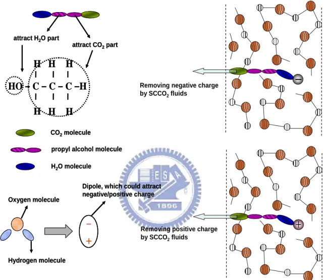
(33) psi-SCCO2 treatment. This exhibits that the SCCO2 treatment possesses excellent ability to passivate the defects, including Hf dangling bonds and interface states. Besides, from Fig. 3-5, the shift of C-V curve under forward and reverse swing is also appears in baking-treated and H2O vapor-treated HfO2 films. It is resulted from the trapped carrier in defects of HfO2 films, and that is not expected for gate insulator of transistors. Under negative gate bias, the electric inject from Al gate into HfO2 films and trapped by defects, leading to the larger gate bias is required for inducing electron-inversion layer. For describing clear, we define the flat-band voltage is the gate bias as C/Cmax = 50%, and the shift of the flat-band voltages under forward and reverse swing is shown in table 3-1. It is evidently observed that the baking-treated HfO2 film hold numerous defects because of the extensive shift of flat-band voltage, and the defects almost disappear after 3000 psi-SCCO2 treatment. These results conform to the tendency in current-voltage characteristics and again verify that the SCCO2 technology could effectively deactivate defects in HfO2 films. Another interesting detection, in Fig. 3-5, is the change of flat-band voltage of different-treated HfO2 films under forward swing, also shown in table 3-1. For baking- treated HfO2 film, the flat-band voltage (= -3.2 volt.) is away from ideal gate bias voltage (about 0~0.3 volt.), and that of 3000 psi-SCCO2 treated HfO2 is zeroed nearly. The main reason could be referred to (1) the positively charged Hf dangling bonds are passivated, (2) the fixed positive charges are removed by SCCO2 fluids. The mechanism of extracting of fixed charge is shown in Fig. 3-6, including positive and negative fixed charge [57]. The polarized-H2O molecule is taken as a dipole which would attract the fixed charge in HfO2 films. Afterward, the H2O molecule and fixed charge are carried away by SCCO2 fluids mixed with propyl alcohol. For H2O. 21.
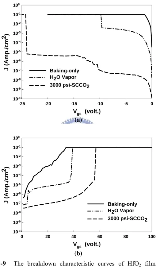
(34) vapor-treated HfO2 film, the un-zeroed flat-band voltage could be attributed to (1) partial positively charged Hf dangling bonds remain, (2) the poorer capability for H2O vapor to remove fixed charge. Hence, it is necessary for H2O molecule to be driven into HfO2 films and carried away by SCCO2 fluids. As a matter of fact, upon reducing the oxide thickness, it is difficult to calculate the density of interface states by using the high-low frequency method because of the substantially increased gate leakage current. Therefore, the interface capacitance (Cit) was employed instead of interface states to investigate the interfacial property. Figure 3-7 (a) and (b) illustrates the equivalent capacitance models of MOS structure without and with Cit, respectively [56]. For higher measuring frequency, fewer interface states could respond to the ac switching signal, so suiting to the model in Fig. 3-7 (a) and presenting lower measured capacitance. For lower measuring frequency, more interface states could respond to the ac switching signal, so suiting to the model in Fig. 3-7 (b) and presenting higher measured capacitance. Therefore, the separation of Cmax under different measuring frequency appears if the interface states existing. Figure 3-8 shows the capacitance-voltage characteristics of HfO2 films after different treatment, measuring at 1M Hz and 100k Hz with forward gate bias swing. A conspicuous separation occurs in baking-treated HfO2 films, and the higher density of interface states is supposed. However, with 3000 psi-SCCO2 treatment, the value of Cmax has only very slight rise under different measuring frequency, proofing that the effectively reducing interface states during SCCO2 process. The sharp slope in transient region of C-V curve thereby is also reasonable.. 3.1.4. Breakdown voltage measurement and gate bias stress. Figure 3-9 (a) and (b) show the breakdown characteristic curves of HfO2 films after various treatments at positive and negative gate bias region, individually. The. 22.
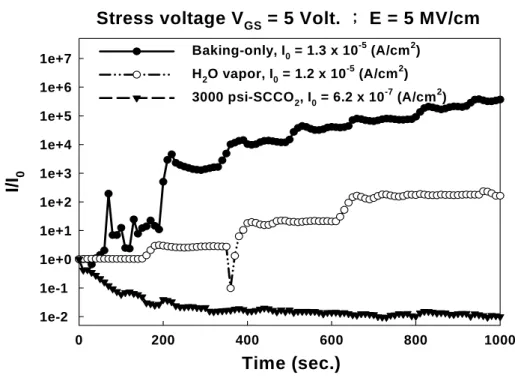
(35) breakdown voltage is mainly relative to the qualities of dielectric films and the density of defects in the dielectric films. A large number of traps lead to the trap-assisted tunneling early occurs and a high leakage current appears at small electric field, such that the lower breakdown voltages of dielectric films comes up. In Fig. 3-10 (a) and (b), whether at negative or positive gate bias, the baking-treated HfO2 film presents the worst performance in breakdown voltage because of the high density of defects, and the improvements of breakdown voltage are gradually achieved via H2O vapor and 3000 psi-SCCO2 treatment. This result exhibits clearly that the density of defects in HfO2 films are effectively reduced, and the breakdown voltage of 7nm HfO2 film thereby could be substantially ameliorated from 1 V to 24 V at negative gate bias, from 30 V to 55 V at positive gate bias. It also indicates that the SCCO2 fluids technology is greatly useful to enhance the low-temperature deposited HfO2 films by passivating defects, and allows the treated HfO2 film holding good reliability as the gate dielectric. Another important property of dielectric films is the reliability under gate bias stress. Due to the gate dielectric is stressed at a high field when the transistors are operating, so that it is demanded for gate dielectric to have excellent resistance to the impairment under long time stress at operating electric field. During high electric field stress, the carriers of leakage current and high electric field would impact the weak bonding, leading to more defects, higher leakage current and the degradation of transistor [58]. Therefore, the reliability of dielectric under gate bias stress would judge whether agrees with the application of gate dielectric. Figure 3-10 shows the variation of leakage current of different-treated HfO2 films as a function of stress time at a high electric field = 5 MV/cm, where I0 is the initial leakage density. As well as the tendency of the measurement of breakdown voltage, the baking-treated HfO2 film. 23.
(36) behaves the most rises in the degree of leakage current as the stress time increasing, because of the great amount of defects and weak bonding. However, after treating with 3000 psi-SCCO2 process, the sputter-deposited HfO2 film performs a fine reliability under high electric field stress, hence it is extremely suitable for the application of gate dielectric.. 3.2. Thin Film Analysis of Material and Discussion. 3.2.1. Fourier Trans-form Infrared Spectroscopy (FTIR) Analysis. Fig. 3-11 shows the FTIR spectra of HfO2 films after various post-treatments, including Baking-only, H2O vapor and 3000 psi-SCCO2 treatment. The functional group referred to Hf-O-Hf bonding is at 509 cm-1 and 690 cm-1, and the absorption peak at around 1070 cm-1 attributes to the Si-O-Si bond. The Si-O-Si bond originates form the formation of interface layer (SiOx) between HfO2 film and silicon wafer during fabricating HfO2 films in Ar/O2 ambient. The peak intensity of Si-O-Si bond for different treatments is almost the same, meaning that these post-treatments would not make different influence on the thickness and quality of the interfacial SiOx film. For the H2O-vapor-treated HfO2 film, however, the peak intensity of Hf-O-Hf bands (509 cm-1 and 690 cm-1) raises apparently in comparison with the baking-only-treated HfO2 film. This is believed well that the H2O vapor would permeate into HfO2 film and makes reaction with Hf dangling bonds (i.e. traps) forming Hf-O-Hf bands. These traps in the low-temperature deposited HfO2 film could be thereby passivated by H2O vapor molecules. Furthermore, with 3000 psi- SCCO2 treatment, obvious increase in the intensity of Hf-O-Hf bonding is observed in the FTIR. It indicates that the best transport efficiency of H2O molecules into HfO2 film is achieved by the SCCO2 fluids, potentially modifying the dielectric properties of HfO2 film, and the transporting. 24.
(37) mechanism for SCCO2 fluids taking H2O molecule into HfO2 film is shown in Fig. 3-12.. 3.2.2. Thermal Desorption System – Atmospheric Pressure Ionization Mass Spectrometer (TDS-APIMS) Analysis. The TDS measurement, as shown in the Fig. 3-13, was carried out upon heating these treated HfO2 films from 50 to 800 °C at a heating rate of 10 °C/min in vacuum (10−5 Pa.). In Fig. 3-13 (a), m/e (mass-to-charge ratio) = 32 peak that is attributed to O2 was monitored to evaluate the content of oxygen outgassing form HfO2 films. It is clearly found the highest oxygen content is detected in the 3000 psi-SCCO2 treated HfO2 film, certainly consistent with the FTIR observation. From Fig. 3-13 (b), m/e (mass-to- charge ratio) = 44 peak that is attributed to CO2, the residual carbon dioxide in HfO2 is equal after various post-treatments. This is result from SCCO2 fluid not only employed to transport the CO2 molecule into HfO2 film but the CO2 molecule is not remain in addition [21, 22].. 3.2.3. X-ray Photoelectron Spectroscopy (XPS) Analysis XPS involves measuring the photoelectron spectra obtained when a sample. surface is irradiated with x-rays. The kinetic energy (peak position) of the photoelectrons can be written as E K = hν -E B -φ s - qφ. (3.12). where hν is the x-ray energy, EB is the binding energy (the difference between the Fermi level and the energy level being measured), φs is the work function of the electron spectrometer, q is the electronic charge, and φ is the surface potential. We have also performed XPS measurements using an Al Kα X-ray source (1486.6 eV photons) to determine the bonding environments of the Hf and O atoms.. 25.
(38) Figure 3-14 shows the O 1s core level peaks also demonstrated binding energy shift with changing of different post-treatments. Each peak can be split into two sub-peaks by Gaussian fitting which represent the Hf-O bonding at ~530.1 eV and O-Si bonding at ~531.5 eV [59,60]. The peak intensity of O-Si bond for different treatments is almost the same, meaning that these post-treatments would not make different influence on the thickness and quality of the interfacial SiOx film. For the H2O-vapor-treated HfO2 film, however, the peak intensity of Hf-O bands raises apparently in comparison with the baking-only-treated HfO2 film. This is believed well that the H2O vapor would permeate into HfO2 film and makes reaction with Hf dangling bonds (i.e. traps) forming Hf-O bands. These traps in the low-temperature deposited HfO2 film could be thereby passivated by H2O vapor molecules. Furthermore, with SCCO2 treatment, obvious increase in the intensity of Hf-O bonding is observed in the XPS. It indicates that the best transport efficiency of H2O molecules into HfO2 film is achieved by the SCCO2 fluids, potentially modifying the dielectric properties of HfO2 film, and the transporting mechanism for SCCO2 fluids taking H2O molecule into HfO2 film is shown in Fig. 3-12.. 3.2.4 Transmission Electron Microscopy (TEM) Analysis Figure 3-15 (a), (b), (c) show the influence of various post-treatments on HfO2 thin film samples in TEM material analysis. The first group labeled as Baking-only treatment, was designed as the control sample, and was only baked on a hot plate at 150 °C for 2 hrs. The second group labeled as H2O vapor treatment, was immersed into a pure H2O vapor ambience at 150 °C for 2 hrs in a pressure-proof stainless steel chamber with a volume of 100cm3. The third group marked as 3000psi-SCCO2 treatment, was placed in the supercritical fluid system at 150°C for 2 hrs, where was. 26.
(39) injected with 3000psi of SCCO2 fluids mixed with 5 vol.% of propyl alcohol and 5 vol.% of pure H2O. The interfacial layer of SiOX for different treatments is almost the same. It is found that 3000psi-SCCO2 treatment can improve performance of MIS, including leakage current density suppression and EOT reduction. On the other hand, the k value of Baking-only-treated, H2O-vapor-treated and 3000psi-SCCO2-treated HfO2 film is about 20.4, 24.8 and 29.4. The k value is increased and interfacial layer is almost the same. It can be understood reasonably that during 3000psi-SCCO2treated HfO2 film is dense and thickness of interfacial layer is increasing a little due to oxygen penetration. The detail discussion would be in 3.1.3.. 3.3. OTFTs Analysis of Electrical Characteristics and Discussion. 3.3.1. The current density-electric field (J-E) characteristics. The leakage current densities of HfO2 films after different treatments are shown as a function of applied negative gate bias voltage to positive gate bias voltage in Fig. 3-16. Among various post-treatments, the baking-treated HfO2 film exhibits the most serious leakage current, inferentially due to its poor dielectric characteristics with numerous traps inside the HfO2 film and the interface between parasitical SiOx and Si wafer. The improvement of electrical characteristics is observed by using H2O vapor process, however, a high leakage current density still appears at larger applied voltages. It could be inferred reasonably dependent on the defect passivation efficiency. The most indicating that H2O vapor can passivate the traps (or defects) and alter dielectric properties of the low-temperature-deposited HfO2 film. After H2O vapor treatment, effective improvement of electrical characteristic is obtained by the 3000 psi-SCCO2 treatment, exhibiting the lowest leakage current density among all samples. Low leakage current density (~2×10⁻⁶ A/cm2) is kept constantly, even biased. 27.
(40) at an electric field of 1.33 MV/cm.. 3.3.2. The capacitance-voltage (C-V) characteristics. The capacitance-voltage (C-V) characteristics are also generally used to judge the quality of dielectric films. Figure 3-17 shows capacitance-voltage characteristics of HfO2 films after different treatment, measuring at 1M Hz with gate bias swing from negative voltage to positive voltage (forward) and from positive voltage to negative voltage (reverse). The slope of C-V curve in transient region, i.e. from Cmax to Cmin, is relative to the interface states, for example, the sharp slope indicates fewer defects exist in the interface between HfO2 and Si wafer. In Fig. 3-17, the baking-treated HfO2 film presents the worst C-V curve and lower capacitance. This expresses the larger number of interface states exist and lead to the smooth C-V curve. With H2O vapor treatment, the sharper C-V curve and higher capacitance are obtained, and it could be attributed to the reduction of defects in HfO2 film and the interface. Furthermore, the best improvement is achieved by 3000 psi-SCCO2 treatment. This exhibits that the SCCO2 treatment possesses excellent ability to passivate the defects, including Hf dangling bonds and interface states. Besides, from Fig. 3-17, the shift of C-V curve under forward and reverse swing is also appears in baking-treated and H2O vapor-treated HfO2 films. It is resulted from the trapped carrier in defects of HfO2 films, and that is not expected for gate insulator of transistors. Under negative gate bias, the electric inject from Al gate into HfO2 films and trapped by defects, leading to the larger gate bias is required for inducing electron-inversion layer. It is evidently observed that the baking-treated HfO2 film hold numerous defects because of the extensive shift of flat-band voltage, and the defects almost disappear after 3000 psi-SCCO2 treatment.. 28.
(41) These results conform to the tendency in current-voltage characteristics and again verify that the SCCO2 technology could effectively deactivate defects in HfO2 films. In another interesting detection, in Fig. 3-17. The baking- treated HfO2 film, the flat-band voltage (= -0.3 volt.) is away from ideal gate bias voltage (about 0~0.3 volt.), and that of 3000 psi-SCCO2 treated HfO2 is zeroed nearly. The main reason could be referred to (1) the positively charged Hf dangling bonds are passivated, (2) the fixed positive charges are removed by SCCO2 fluids. The mechanism of extracting of fixed charge is shown in Fig. 3-6, including positive and negative fixed charge [57]. The polarized-H2O molecule is taken as a dipole which would attract the fixed charge in HfO2 films. Afterward, the H2O molecule and fixed charge are carried away by SCCO2 fluids mixed with propyl alcohol. For H2O vapor-treated HfO2 film, the un-zeroed flat-band voltage could be attributed to (1) partial positively charged Hf dangling bonds remain, (2) the poorer capability for H2O vapor to remove fixed charge. Hence, it is necessary for H2O molecule to be driven into HfO2 films and carried away by SCCO2 fluids.. 3.3.3. Secondary Ions Mass Spectrometer (SIMS) Analysis. The means of secondary ion mass spectroscopy (SIMS) analyzed by using various elements profiles in the dielectrics. During SIMS analysis [61], the surface of the sample is subjected to Cs+ ion bombardment with energy of 5.78 KeV and negative secondary ions. The bombarding primary ion beam (Cs+) produces monatomic and polyatomic particles of sample material and re-sputtered primary ions, along with electrons and photons. This leads to the ejection of both neutral and charged species from the surface. Monitoring the secondary ion count rate of the selected element as a function of time leads to depth profiles.. 29.
數據
+7
相關文件
For importation of cinema film, no matter whether the film is positive or negative, an approval issued by Bureau of Audiovisual and Music Industry Development, Ministry of Culture
You are given the wavelength and total energy of a light pulse and asked to find the number of photons it
Wang, Solving pseudomonotone variational inequalities and pseudocon- vex optimization problems using the projection neural network, IEEE Transactions on Neural Networks 17
Hope theory: A member of the positive psychology family. Lopez (Eds.), Handbook of positive
volume suppressed mass: (TeV) 2 /M P ∼ 10 −4 eV → mm range can be experimentally tested for any number of extra dimensions - Light U(1) gauge bosons: no derivative couplings. =>
Define instead the imaginary.. potential, magnetic field, lattice…) Dirac-BdG Hamiltonian:. with small, and matrix
• Formation of massive primordial stars as origin of objects in the early universe. • Supernova explosions might be visible to the most
• Density is varying in the medium and the volume scattering properties at a point is the product of scattering properties at a point is the product of the density at that point
