行政院國家科學委員會專題研究計畫 成果報告
氮化鎵族面射型垂直共振腔發光元件之開發
計畫類別: 個別型計畫 計畫編號: NSC93-2215-E-009-068- 執行期間: 93 年 08 月 01 日至 94 年 07 月 31 日 執行單位: 國立交通大學光電工程學系(所) 計畫主持人: 王興宗 共同主持人: 郭浩中 計畫參與人員: 博士生-姚忻宏,碩士生-游敏,許意偵,葉剛帆 報告類型: 精簡報告 處理方式: 本計畫可公開查詢中 華 民 國 94 年 11 月 1 日
行政院國家科學委員會補助專題研究計畫
■ 成 果 報 告
□期中進度報告
氮化鎵族面射型垂直共振腔發光元件之開發
計畫類別:■ 個別型計畫 □ 整合型計畫
計畫編號:NSC 93-2215-E-009-068-
執行期間:93 年 08 月 01 日至 94 年 07 月 31 日
計畫主持人:王興宗 教授
共同主持人:郭浩中 副教授
計畫參與人員:
博士生-姚忻宏
碩士生-游敏,許意偵,葉剛帆
成果報告類型(依經費核定清單規定繳交):■精簡報告 □完整報告
本成果報告包括以下應繳交之附件:
□赴國外出差或研習心得報告一份
□赴大陸地區出差或研習心得報告一份
□出席國際學術會議心得報告及發表之論文各一份
□國際合作研究計畫國外研究報告書一份
處理方式:除產學合作研究計畫、提升產業技術及人才培育研究計畫、
列管計畫及下列情形者外,得立即公開查詢
□涉及專利或其他智慧財產權,□一年□二年後可公開查詢
執行單位:國立交通大學光電工程研究所
中 華 民 國 94 年 10 月 31 日
1
Development of Fabrication Process for Nitride-based
Vertical Cavity Surfaced Light Emitting Devices
氮化鎵族面射型垂直共振腔發光元件之開發
總執行期限:2004/08/01 ~2005/07/31PI:S. C. Wang(王興宗), National Chiao-Tung University, E-mail: [email protected] Co-PI:H. C. Kuo (郭浩中)
Abstract
We have accomplished the objectives of this project. The main accomplishments include successfully fabrication of GaN vertical cavity surface emitting laser (VCSEL) structure, the achievement of lasing action of GaN VCSEL, and the fabrication of GaN-based micro-cavity device.
摘要
我們已按本計畫預期之進度順利完成此計畫目的。包括成功製造出氮化鎵面射型雷射結構 、達到氮化鎵面射型雷射的雷射操作、以及氮化鎵微共振腔元件的製造與分析。報告內容
(一) 前言 本文為奈米國家型科技計畫之氮化鎵面射型垂直共振腔發光元件之開發之精簡成 果報告,內容為簡介本計畫一年所研究之實驗方法、成果以及所發表之文獻。 (二) 研究目的 本計畫預計完成之工作為建立最佳的磊晶條件及製作高反射率的短波長 DBR 結 構、建立元件製作技術以及氮化鎵垂直共振腔面射型發光元件製作及元件特性量測技 術之建立。 (三) 文獻探討 在半導體III-nitride 材料 DBR 結構的研究上,美國新墨西哥州的 Sandia 國家實驗 室Figiel 等人在西元 2001 年成長了 Al0.20Ga0.80N/GaN DBR 的結構[1]。其結構中每隔20 對 Al0.20Ga0.80N/GaN 便嵌入一層多晶系(amorphous) AlN 得以鬆弛 (release)由於晶
格不匹配所產生的應力,得到了60 對 Al0.20Ga0.80N/GaN DBR 之中心波長為 378 nm,
反射率為99.1%,但是由於 AlGaN 的 Al 含量只有 20%,折射率差異極小,因此需 要60 對才能得到如此高的反射率,且其 stopband 僅有 10nm 左右。西元 2000 年,
美國波士頓大學電資學院的H.M.Ng 等人利用 MBE 成長了 20.5~25.5 對的 AlN/GaN DBR 結構[2],其反射率可高達 99%,stopband 的寬度更高達 45 nm(中心波長約在 470 nm),且此20.5 對的 AlN/GaN DBR 結構顯示並沒有晶格崩裂的現象。西元 1999 年 , 日 本 東 京 大 學 的 荒 川 泰 彥 等 人 利 用 MOCVD 磊 晶 的 方 式 在 40 對 的 Al0.34Ga0.66N/GaN DBR 的結構上面成長了 2.5λ cavity 的氮化銦鎵(InGaN)量子井結構
[3],之後在其上鍍上了數對 HfO2/SiO2氧化物DBR 結構,並達到光激發雷射操作;
西元2000 年美國布朗大學 Y-K Song 等人利用 Laser left-off 的技術將 sapphire 基板與 氮化銦鎵量子井薄膜結構分離,之後在薄膜的上下方鍍上10 對的 HfO2/SiO2 DBR 結
構,也得到高品質共振腔並達到光激發雷射操作[4],Y. K. Song 等人甚至將此一結 構實際元件化,做成相當接近雷射輸出的共振腔發光元件[5]。
(四) 研究方法、結果與討論
(1) Vertical cavity surface emitting laser (VCSEL) is successfully fabricated.
1. Successfully fabrication of VCSEL structure with high-reflectivity GaN/AlN DBR and Ta2O5/SiO2 DBR.
The GaN VCSEL structure with high-reflectivity AlN/GaN distributed Bragg reflector (DBR) and Ta2O5/SiO2 DBR were realized by metal organic chemical vapor
deposition (MOCVD). The full structure consists of a 25-pairs AlN/GaN DBR, a 380-nm-thick n-type GaN, a ten pairs In0.2Ga0.8N/GaN MQW, a 100-nm-thick p-type,
and a 8-pairs Ta2O5/SiO2 DBR.The SEM picture is shown in Fig.1. The highest peak
reflectivity of AlN/GaN DBR is about 94.5% with a stopband width of 18nm at a center wavelength of 442nm(Fig.2). The eight pairs Ta2O5/SiO2 dielectric mirror showed
about 97.5% reflectivity was deposited by the e-gun as the top DBR reflector. Fig.3 shows the PL spectrum from the GaN-based VCSEL at the room temperature. A narrow emission peak with full width at half maximum of 1.4nm corresponds to the cavity resonant mode at 448nm was observed. It indicates the emission peak was well-aligned with vertical cavity formed by the high reflectance of AlN/GaN DBR and the
Ta2O5/SiO2 dielectric mirror. The cavity quality factor estimated from the emission
linewidth of 1.4nm is about 320. This high Q value means the resonant cavity of nitride VCSEL is successfully fabricated.
Fig. 1 SEM picture of nitride VCSEL. Fig. 2 The reclectivity of top and bottom DBRs
350 400 450 500 550 0 20 40 60 80 100 AlN/GaN DBR Ta2O5/SiO2 DBR Reflectivity (% ) Wavelength (nm) 425 430 435 440 445 450 455 460 465 0 50 100 150 200 250 300 1.4nm Inte ns ity (a.u .) Wavelength (nm)
3
2. The lasing action of niride based vertical cavity surface emitting laser was achieved. The VCSEL has been successfully optically pumped to achieve lasing action at room
temperature. The optical pumping of the sample was performed using a frequency-tripled Nd:YVO4 355-nm pulsed laser with a pulse width of ~ 0.5 ns at a repetition rate of 1 kHz.
Fig. 4(a) plots the light emission intensity from the VCSEL as a function of the pumping energy. The laser action was observed as the pumping energy above the threshold pumping energy (Eth) of about 1.5µJ corresponding to an energy density of 53mJ/cm2A.
The Fig. 4(b) shows the emission image of GaN VCSEL. With the pumping energy increasing, the bright laser spot appears, and its size is about 3μm. The laser output also increased linearly and rapidly with the pumping energy beyond the threshold. Fig 4(c) shows the variation of emission spectrum with the increasing pumping energy. The dominant laser emission line is located at 448nm above the threshold pumping energy. The laser emission spectral linewidth reduces with the pumping energy above the threshold energy and approaches 0.25nm at the pumping energy of 2.52Eth. These
characteristics strongly suggest the achievement of the lasing action.
2. The GaN-based micro-cavity device with nitride VCSEL structure is fabricated.
(b)
Fig. 4. (a) the threshold characteristic of GaN VCSEL. (b) the emission image of the laser. (c) the emission spectra of GaN VCSEL below and above the threshold.
0 1 2 3 4 5 0 2000 4000 6000 8000 10000 Em ission Inten s ity (a. u .)
Excitation Energy (µJ/pulse)
(a)
430 440 450 460 470 0.25nm 2.52 Eth 1.64 E th 1.38 Eth 0.75 Eth 1.13 Eth In te ns it y (a .u .) Wavelength (nm)(c)
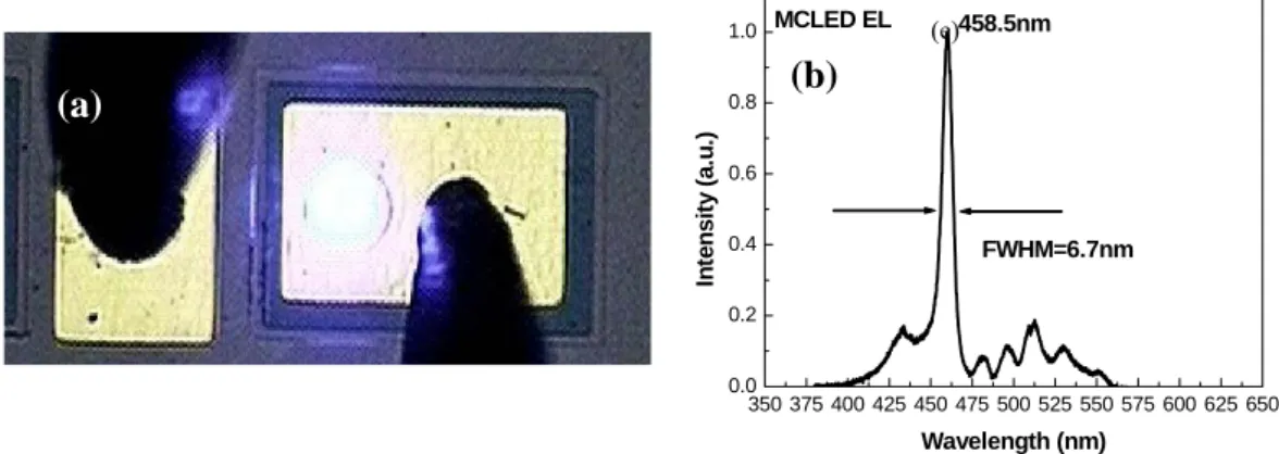
The micro-cavity device using the VCSEL structure has been fabricated. The emission picture of the device is shown in Fig. 5(a). The device shows strong emission intensity in the aperture region. The emission spectrum is measured as shown in Fig. 5(b). The emission peak is located at 458.6nm with a narrow linewidth about 6.7nm. The linewidth narrowing was caused by the resonant cavity effect. The low thermally induced red-shift effects (0.12 nm/kA/cm2) were also observed by varying the injection current density and temperature. These characteristics fully suggest this device has the performance similar to the VCSEL and could be a basis for the goal of electrically pumped VCSEL.
(五) Reference(參考文獻)
[1] Figiel et. al., Appl. Phys. Lett., vol. 78, p. 3205, 2001. [2] H. M. Ng et. al., Appl. Phys. Lett., vol. 76, p. 2818, 2000. [3]T. Someya, Science, vol 285, p. 1905 (1999)
[4]Y. K. Song et. al. , Appl. Phys. Lett., vol.74, p. 3441, 1999 [5] Y. K. Song et. al., Appl. Phys. Lett., vol.77, p. 1744, 2000 本實驗室已發表之相關論文
[1]Chih-Chiang Kao, Y. C. Peng, H. H. Yao, J. Y. Tsai, Y. H. Chang, J. T. Chu, H. W. Huang, T. T. Kao, T. C. Lu, H. C. Kuo, and S. C. Wang, and C. F. Lin, Appl. Phys. Lett. 87, 081105 (2005) 相關畢業論文 [2] Y. C. Peng(彭裕鈞), 氮化鎵面射型雷射及微共振腔元件之研究,交大光電所 93 碩士畢業論文 (六) 計畫成果自評 本計畫預定目標如下: 1.建立最佳的磊晶條件及製作高反射率的短波長 DBR 結構 2.建立元件製作技術。包括雷射剝離藍寶石基板技術、透明電極、ITO 及 ICP 等製程 技術以提升發光元件之發光效率。 3.氮化鎵垂直共振腔面射型發光元件製作及元件特性量測技術之建立。 4.氮化鎵量子點在光學微共振腔結構中之光電特性分析並比較得到最佳之元件結構。 在相關研究人員包括所有計畫共同主持人、博士後研究員、博碩士生在這一年的努
Fig. 5 (a) The emission images of GaN-based micro-cavity device. (b) The EL spectrum of the micro-cavity device device.
(d) (e) (a) 350 375 400 425 450 475 500 525 550 575 600 625 650 0.0 0.2 0.4 0.6 0.8 1.0 MCLED EL FWHM=6.7nm 458.5nm In te n s it y (a .u .) Wavelength (nm) (b)
5 力之下,才能有此豐富的成果報告,包括成功利用有機化學氣相沈積系統成長高反射 率之氮化鋁/氮化鎵多層反射膜、製造高品質之氮化鎵面射型雷射結構、達到氮化鎵雷 射之雷射操作、以及氮化鎵微共振腔發光元件之設計與製作,所以與原計畫所預定的 目標相符程度大約有八成以上,加上所發表的學術論文及國際期刊,目前之成果可說 是已經和外國學術研究並駕齊驅。