The
Improved Stability
of
Deuterated Amorphous Silicon Thin Film Transistor
Jeng-Hua Wei and Si-Chen LeeDepartment of Electrical Engineering, National Taiwan University, Taipei, Taiwan, China
Abstract
In order to reduce the bias-induced degradation in hydrogenated amorphous silicon thin film transistor (a-Si:H TFT), a deuterated amorphous silicon layer prepared by deuterium plasma treatment is used as the active layer. It is demonstrated that the stability, i.e., the shifts of threshold voltage and subthreshold swing, of deuterated amorphous silicon thin film transistor can be indeed improved as compared to the hydrogenated ones. This result is consistent with the improvement of the light-induced degradation in deuterated amorphous silicon film and this improvement can be explained by the efficient coupling between Si-D wagging mode and amorphous silicon phonon mode.
I. Introduction
Hydrogenated amorphous silicon thin film transistor (a-Si:H TFT) has wide used in many different areas [I], and the most important application is the active-matrix liquid crystal display (AMLCD) However, the instability of a-Si:H TFTs is the long-lasting problem constraining its !usability. This instability comes from two sources: one is the charge trapping inside the insulating layer, i.e., silicon nitride a-SiN,:H [Z]; the other is the creation of metastable defects, i.e., silicon dangling bonds, in the a-Si:H which increase the interface states at the a-Si:Winsulator interface. Therefore, it seem quite straight forward to improve the TFT stability in two ways: first, optimizing the silicon nitride quality in order to reduce the trapped charge effect; second, improving the a-Si:H structure to reduce the creation rate of Si metastable defects under bias. The creation of metastable defect in a-Si:H was known for a long time. In 1977, it was first observed that the extended illumination of a-Si:H with visible light produced a decrease in photoconductivity (the Staebler-Wronski effect) [j]. This degradation becomes one of the most important topics in the studies of a-Si:H material and it is found the degadation is due to the increase of the metastable defects in the films. It is also found that the metastable defects can be created by the charge injection (forward bias) or temperature stress [4,
51. Therefore, if we can find a method to reduce the degradation of the a-Si.H under illumination, the degradation of a-Si:H TFT under bias may also be slowed down.
In 1995, the hot electron degradation in Si metal oxide semiconductor transistor (MOSFET) has been found to be greatly reduced by passivating the Si/Si02 interface with deuterium instead of hydrogen [6]. In 1997, Sugiyama ef al. [7] have demonstrated that an a-Si:D solar cell is more stable than an a-Si:H cell under normal operation and our group has also demonstrated that an a-Si:D film is more stable than an a-Si:H film under illumination and proposes a possible model to explain this improvement [SI. Since the creation mechanism of metastable states in the channel region of a-Si:H or a-Si:D TFTs by the hot electrons is similar to the creation of metastable states in the a-Si:H(D) films by illumination. It is expected that the a-SkD TFT may also exhibit the lower creation rate of metastable states in the channel and the device degradation could be improved. In this paper, it is demonstrated that the degradation of a-Si:D TFT is indeed improved as compared to the hydrogenated ones.
I1 Experiments
Figure 1 displays the fabrication processes of the amorphous silicon TFTs. The substrate used is Coming 7059 glass. First, the 80 nm Cr was evaporated on the glass substrate and the SO tun thick n' a-Si:H was deposited on the Cr
as
shownin
Fig. l(a). After deposition, the n+ a-Si:H was etching by reactive ion etching (ME) and Cr metal was patterned by wet etching to form the contact pad of the TFTs as shown in Fig. l(b). Before removing the photoresist (PR) on the n+ a-Si:H, a liquid phase deposited silicon dioxide (LPD-SiOl) was grown to planarize the surface [9]. The preparation procedures of LPD-Si02 solution are described elsewhere [9]. The samples were immersed in the growth solution to grow tne Si01 until the step between n' a-Si:H and glass substrate is filled up as shown in Fig. l(c). A 100 nm a-Si:H was deposited after removing the PR as shown in Fig. I(d). This a-Si:H is used as the active layer in the TFTs. Then the D2 or H2 plasma treatment processes were used to treat the a-Si:H84
3
n+a-Si:H
(a)
LPD-Si02
fDhotoresist
(b)
I
a-Si:Wa-Si:Dn
+
a
-
s
i
:
F
-[Cr
7059
Glass
(f)Figure 1 The flow chart of the TFT fabrication processes.
layers. The procedures of plasma treatment processes are as follows: the a-Si:H films were annealed at 550°C in N2 environment for 5 minutes to expel all the hydrogen atoms out of the films. Then the annealed films were treated separately by HI and DI plasma until
their electrical properties (dark and photoconductivities) were recovered. The plasma' treatment conditions are followings: substrate temperature 300"C, chamber pressure 6 torr, gas flow rate 3 sccm, power density 0.1 Wicm' and the treatment time 3 hours. Three different active layers were prepared , i. e., the as-deposited a-SilH, plasma treated (PT) a-Si:H and plasma treated (PT) a-Si:D. Then the active layers were mesa etching by RIE as shown in Fig. I(e) to reduce the gate leakage current from the gnte electrode to the sourceldrain electrodes. The etching condition are: CFn 36.5 sccm,
Ot 4 sccm, pressure 30 mtorr and the power density 0.4 ' W/cm'. After etching, a 200 nm LPD SiOl was deposited at 50°C and the gate electrode (AI with 1% Si)
was vacuum evaporated and patterned. The final TFT device structure was shown in Fig. I(@ The current-voltage characteristics of the three types of TFTs were measured, their o d o f f current ratio, threshold voltage, subthreshold swing, efc., were extracted. Then the TFTs were stressed by varying the gate (V,) and drain (V,) bias from 0 to 40 V. The stress time was varied from 500 to 10000 seconds. After stress, the changes of threshold voltage and subthreshold swing of
the TFTs were recorded and compared to find out the most stable devices.
111. Results and Discussion
The drain current (Id) versus drain voltage (Vds)
characteristics of as-deposited a-Si:H, PT a-Si:H and PT a-Si:D TFTs are shown in Figs. 2 (a), (b) and (c), respectively. Apparently the a-Si:D TFT exhibits :he
1 0 x1061
-
1
As-deposited a-Si:H TIT i5 I
Drain Voltage. Vds (Volt) '1.0 x 1 O 6 r
-
1 PTa-Si:HTFT ' 4 0-
-
vc=20v - 6 s (b)2
0.5 XI0,
5 4:
IO 5 0 0 IO 15 20Drain Voltage. Vds (Volt) 1.5 x10⁶
I
-
5 vc=20vg
4
1.0 X l d (C)$
c 0 . 5 ~ 1 6 ~ 1E
10 5 0 0 10 15 20Drain Vallage. Vds &'oil) Figure 2 Drain current (1.) versus drain Voltage (V,) characteristics of (a) as-deposited a-Si:H, (b)
PT a-Si:H and (c) PT a-Si:D TFTs before bias stress.
844
highest drain current at the same gate and drain biases. The relation between square root of Id and Vd. of the same TFT biased in the saturation region (V, = V,) are shown in Fig. 3 (a). The field effect mobility evaluated from the slope are about 0.13, 0.14 and 0.20 cm*N-sec for the as-deposited a-Si:H, PT a-Si:H and PT a-Si:D TFTs, respectively. These are the typical value for TFT with SiO? as the gate insulator. The threshold voltage obtained from the intercept of V& axis is about 5.2, 4.3 and 3.8 V for the as-deposited a-Si:H, PT a-Si:H and PT a-Si:D TFTs, respectively. Because the LPD-SiO? is
c! - 3 (a)
?3
c! - 2 I , 0_ . - . .
_..-...
0.4 10 20Next, the stabilities of a-Si:H and a-Si:D TFTs were tested under V, = V,, = 20 V. The stress time varies
t?om t = 500 to 10000 seconds in seven steps. During the bias stress, threshold voltage shift (AVT) and the subthreshold swing shift (AS) are extracted kom the experiment data.
First, Figs. 4 (a) and (b) replot the threshold voltage and subthreshold swing shift of the as-deposited a-Si:H, PT a-Si:H and PT a-Si:D TFTs after V, = Vdt 320 V
Drain Voltage, Vds (Volt)
l o 5
7
1
4 3 1
I
10 -10 0 10 20
Gate Voltage, Vgs (Volt)
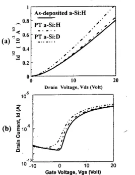
Figure 3 (a) Relation between square root of I d and gate bias (V,) and (b) transfer curves of as-deposited a-Si:H, PT a-Si:H and PT a-Si:D TFTs with Va. = V,.
grown near the room temperature ( 50°C ), the defect, state density inside the LPD-SiO? is larger than that in SiO? grown at high temperature. The threshold voltages of three TFTs are thus expected to be slightly higher than the value of normal TFT. Figure 3 (b) shows the transfer curve of above three TFTs with V, = 10 V, respectively. The o d o f f current ratio are about 5 order of magnitude and the subthreshold swing are about 1.5 V/decade for the three TFTs. These device parameters demonstrate that they are good quality TFTs with Si02 as the gate insulator.
v d s =
20v
6
%!,
1,000 2,000 5,000 tO,!JOO Stress i l n e , t (second)2
1.2a
2 . 1 a,*PT a-Si:H
.*PT a-Si:D
~*a-Si:H
a n o t ' 'I
500 1,000' 2,000 5,000 10,000 Stress Time, t (second)Figure 4 The (a) threshold voltage and (b) subthreshold swing shifts of the as-deposited a-Si:H
(U),
plasma treated (PT) a-Si:H(0)
and a-Si:D(0)
TFTs. The.stress condition is V, = 20 V, Vb = 20 V and the stress time varies from t = 500 to 10000 secondsstress for 500 to 10000 seconds. After 10000 second stress, the threshold voltage shift of the as-deposited
845
a-Si:H, PT a-Si:H and PT a-Si:D TFTs are 6.94, 5.45 and 3.65 V, respectively. The shift of a-Si:D TFT is the lowest. For the subthreshold swing, the shifts of the as-deposited a-Si:H, PT a-Si:H and PT a-Si:D TFTs are 0.629. 1.10 and 0.5 12 Vldecade. Again, the a-Si:D TFT has the lowest shift.
In a-Si:H(D) TFT. the sources of the threshold voltage shift are the charges trapped inside the gate insulator and the interface states created by increasing the metastable states in the a-Si:H(D) layer [IO]. Form experimental results described in above sections, it is found that the a-Si:D TFT has the lowest threshold voltage shift under five different stress conditions. Because the gate insulator (LPD-SO?) of three TFTs are the same, their fabrication procedures are also the same. The improved stability of a-Si:D TFT is indeed due to the lower metastable states created in the a-Si:D active layer. After the same stress time (IO000 seconds), the a-Si:D TFT also shows the smallest shift in subthreshold swing among three different samples. The shift of subthreshold swing is *elated to the density of defect states at the insulator /a-Si:H(D) interface by bias stress [ 18,191. Therefore, the experimental data indicates that the a-Si:D film is the most stable one under bias stress like the case under light exposure.
V. Conclusions
A good quality a-Si:D TFT using plasma treatment method is demonstrated. The threshold voltage is 3.8 V.
3 the field effect mobility at the saturation region is 0.16
cmW-sec, the odoff current ratio is about 5 order of magnitude and the subthreshold swing is 1.5 V/decade. From the measurement of different stress conditions, it is found that the PT a-Si:D TFT is the most stable one as compared to the as-deposited and PT a-Si:H TFTs. The stability of amorphous silicon TFT can indeed be improved by using deuterium atoms to replace hydrogen atoms. This is consistent with the conclusions of the light-induced degradation in our previous paper [8]. References
I . M. Kinugawa, Thin Film Transistor Technologies, p. 2. M. J. Powell, lEEE Tran. Electron Devices, 36, 2753,
I45 (1 992). (1989).
3. D. L. Staebler and C. R. Wronski, Appl. Phys. Lett., 31,291 (1977).
4. M. Stutmann, W. B. Jackson and C. C. Tsai, Phys.
5. R. A. Street, Appl. Phys. Lett., 59, 1084 (1991). 6. J. W. Lyding , K. Hess and 1. C. Kiziyalli, Appl. Phys.
7. S . Sugiyama, Y. Yang and S . Guha, Appl. Phys. Lett., 8 . J . H. Wei, M. S . Sun and S . C. Lee, Appl. Phys. Leu..
9. J. S . Chou and S . C. Lee, Appl. Phys. Lett., 64, 1971
IO. C. van Berkel and M. J. Powell, Appl. Phys. Lett.,
Rev. B, 32,23 (1985). Lett., 68,2526 (1996) 70,378 (1997). 71, 1498 (1997). ( 1994). 51, 1094 (1987).