Effective density-of-states distribution of polycrystalline silicon thin-film transistors
under hot-carrier degradation
Ming-Hsien Lee, Kai-Hsiang Chang, and Horng-Chih Lin
Citation: Journal of Applied Physics 102, 054508 (2007); doi: 10.1063/1.2777804
View online: http://dx.doi.org/10.1063/1.2777804
View Table of Contents: http://scitation.aip.org/content/aip/journal/jap/102/5?ver=pdfcov Published by the AIP Publishing
Articles you may be interested in
Thermal analysis of amorphous oxide thin-film transistor degraded by combination of joule heating and hot carrier effect
Appl. Phys. Lett. 102, 053506 (2013); 10.1063/1.4790619
Effects of grain boundaries on performance and hot-carrier reliability of excimer-laser annealed polycrystalline silicon thin film transistors
J. Appl. Phys. 95, 5788 (2004); 10.1063/1.1699504
Anomalous hot-carrier-induced degradation of offset gated polycrystalline silicon thin-film transistors Appl. Phys. Lett. 84, 3163 (2004); 10.1063/1.1707222
Photon emission and related hot-carrier effects in polycrystalline silicon thin-film transistors J. Appl. Phys. 85, 6917 (1999); 10.1063/1.370105
Determination of hot-carrier induced interface state density in polycrystalline silicon thin-film transistors J. Appl. Phys. 84, 2341 (1998); 10.1063/1.368302
Effective density-of-states distribution of polycrystalline silicon thin-film
transistors under hot-carrier degradation
Ming-Hsien Lee and Kai-Hsiang Chang
Institute of Electronics, National Chiao Tung University, Hsinchu, Taiwan 300, Republic of China
Horng-Chih Lina兲
Institute of Electronics, National Chiao Tung University, Hsinchu, Taiwan, Republic of China and National Nano Device Laboratories, Hsinchu, Taiwan 300, Republic of China
共Received 24 May 2007; accepted 20 July 2007; published online 11 September 2007兲
In this work, quantitative information for nonuniform hot-carrier degradation, especially under mild stressing condition, is investigated. A test structure capable of revealing hot-carrier degradations of polycrystalline silicon共poly-Si兲 thin-film transistors in specific portions of the channel is employed. Effective density-of-states 共DOS兲 distributions at the damaged sites can be extracted using field-effect conductance method, thus providing an effective tool to evaluate the impact of hot-carrier degradations. By measuring along individual sections of the channel, it becomes possible to extract the DOS for the device as a whole. The combination of the proposed test structure and DOS extraction technique also provides a powerful tool for modeling and simulating current-voltage characteristics of thin-film transistors under hot-carrier stressing. © 2007 American Institute of
Physics.关DOI:10.1063/1.2777804兴
INTRODUCTION
Polycrystalline silicon 共poly-Si兲 thin-film transistors 共TFTs兲 have been extensively used in many applications, es-pecially for active-matrix liquid-crystal displays 共AMLCDs兲.1–4
Because of their better crystallinity, com-pared with the amorphous counterparts, significant improve-ment in device performance in terms of carrier mobility and drive current can be realized in poly-Si TFTs. Along with these improvements, the stability and reliability of the poly-Si TFTs now become a major issue. Hot-carrier degra-dation remains as one of the most critical concerns for prac-tical applications.5,6Hot carriers are induced by high electric fields in the channel. By releasing their energy, these hot
carriers could generate defects and cause device
degradation.7Since the electric field along the channel is not uniformly distributed, hot-carrier-induced damage is location dependent along the channel. Because of the lack of sub-strate contacts, coupled with the presence of numerous inter-/ intragrain defects,8the whole picture is much more compli-cated for poly-Si TFTs, compared with bulk metal-oxide-semiconductor field-effect transistors 共MOSFETs兲. The damage scenarios of hot-carrier degradations have been char-acterized in the literature by a number of techniques, includ-ing reversed source/drain measurement,9capacitance-voltage 共C-V兲 measurement,10
device simulation,11,12 asymmetric drain/source structure,9 and picosecond time-resolved emis-sion microscope.13 However, none of the above methods is capable of directly and unambiguously pinpointing the dam-age location.
Modeling hot-carrier degradations is a challenging task. Trap states associated with grain boundaries, intragranular defects, and hot-carrier induced defects can be taken into
account through the use of the effective density-of-states 共DOS兲 distribution within the band gap.14–17
However, real-istic DOS distribution is very difficult to obtain owing to the nonuniform distribution of induced defects by the hot-carrier stressing. Recently, a test structure capable of spatially re-solving the damage along the channel of the stressed transis-tor has been proposed by our group.18 With the proposed structure, analysis of hot-carrier degradation along the stressed channel becomes feasible. In this work, modeling of the location-dependent hot-carrier degradation is investigated in detail using the proposed structure. We show that, by mea-suring along individual sections of the channel, it becomes feasible to extract the DOS for the device as a whole.
DEVICE EXPERIMENTAL AND SIMULATION
The test structure was originally designed to spatially detect and reveal the location of damage sites during hot-carrier stressing. The top view of the test structure is illus-trated in Fig. 1共a兲. One test transistor along the x direction, denoted as TT, is designed to receive the hot-carrier stress-ing. Three monitor transistors 共MTs兲 along the y direction, denoted as S-MT, C-MT, and D-MT, respectively, can be characterized independently before and after the stressing. In this way, damage induced at different portions of the channel can be directly resolved. Figures1共b兲and 1共c兲 illustrate the schematics of the test transistor and monitor transistors, re-spectively.
Because the proposed test structure requires only modi-fications in layout, the processing steps are identical to those of conventional TFTs. No extra masks or lithography steps are needed when employing the test structure. TFTs in this work were prepared on oxidized Si wafers with a 50-nm-thick polycrystalline silicon layer to serve as the ac-tive device region. The polycrystalline silicon layer was formed by depositing an amorphous silicon layer and then
a兲Electronic mail: [email protected]
0021-8979/2007/102共5兲/054508/6/$23.00 102, 054508-1 © 2007 American Institute of Physics [This article is copyrighted as indicated in the article. Reuse of AIP content is subject to the terms at: http://scitation.aip.org/termsconditions. Downloaded to ] IP:
crystallizing it at 600 ° C in N2 for 24 h. Afterwards, a 35-nm-thick tetra-ethyl-ortho-silicate 共TEOS兲 and 200-nm-thick n+ poly-Si were deposited and patterned to form the gate dielectric and gate electrode, respectively. Standard processing for source/drain formation, passivation, and metallization were then performed, followed by a plasma treatment in NH3 ambient at 300 ° C for 1 h.
The effective DOS distribution in the device channel was extracted from the subthreshold current-voltage 共I-V兲 characteristics using the field-effect conductance 共FEC兲 method.19The method was originally proposed by Suzuki et
al. for amorphous silicon films.20 Later Fortunato and Migliorato applied the method to poly-Si films.21 This method assumes that spatial distribution of the defect states along the channel is uniform, which is acceptable when the grain size of poly-Si film is small. The DOS at a given en-ergy level inside the band gap can be expressed as
DOS共EF+s兲 = Si 2q 2 s 2
冉
冏
d dx冏
x=0冊
2 . 共1兲In Eq. 共1兲, EF,s, andSi represent Fermi energy, sur-face band bending at the channel/gate-oxide intersur-face, and dielectric constant of the silicon, respectively. In this work, incremental method22 is employed to construct the relation-ship between the measured current-voltage characteristics and the surface band bending. The relationship can be ob-tained by the following equation:
s,i+1=s,i+ ID,i+1− ID,i ID,flatband d t0x 0x Si VG,i− VFB−S,i exp共qSi/KT兲 − 1, 共2兲 where d represents the thickness of the poly-Si channel. Us-ing the initial condition 共i.e., S,i=0= 0兲 and the known
current-voltage 共ID,iand VG,i兲 relationship, we can calculate
the correspondingS,ifor a specific VG,i. The DOS at a given
energy level can then be calculated using Eq.共1兲. Note that only DOS distribution of the energy level above the Fermi
energy 共E⬎EF兲 can be extracted because n-type TFTs are
used in this work.
RESULTS AND DISCUSSION
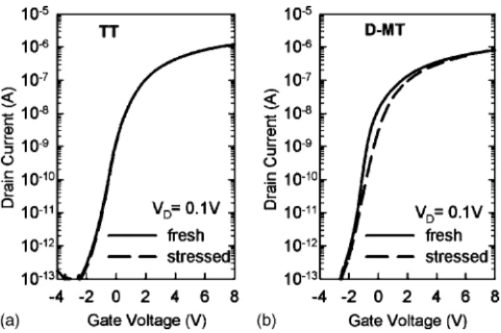
Owing to the nature that hot-carrier degradation is usu-ally occurred at some portions of channel, it is very difficult to observe the degradation in subthreshold characteristics when the stress condition is moderate. Figure 2共a兲 shows subthreshold characteristics of a test transistor measured at drain voltage 共VD兲 of 0.1 V, before and after a moderate
hot-carrier stressing, under gate voltage 共VG兲 of 6.5 V and
VDof 13 V for 1000 s. In this case, hot-carrier degradation
cannot be observed by the subthreshold characteristics be-cause the damaged region is very small compared with the whole channel. In our previous work,23the damaged region under such stress condition was found to be located near the drain side. As shown in Fig.2共b兲, visibly retarded I-V char-acteristics of the monitor transistor near the drain 共D-MT兲 directly and clearly reveal the existence of the damaged area near the drain side. The information from the D-MT can provide excellent sensitivity in characterizing the hot-carrier degradation.
For traditional testers, trying to resolve the difference in effective DOS distribution during hot-carrier degradation is more arduous, especially when the device is stressed under moderate or mild conditions. For example, Fig.3shows and compares the effective DOS distributions of the test transis-tor characterized in Fig. 2共a兲 before and after a moderate hot-carrier stressing of VG/ VD= 6.5 V / 13 V for 1000 s. As
can be seen in the figure, it is very difficult to distinguish the difference of effective DOS induced by the hot-carrier deg-radation. This is because only a small portion of the channel is damaged; the increased DOS will be averaged out during the extraction owing to the assumption that spatial distribu-tion of defect states along the channel is uniform.
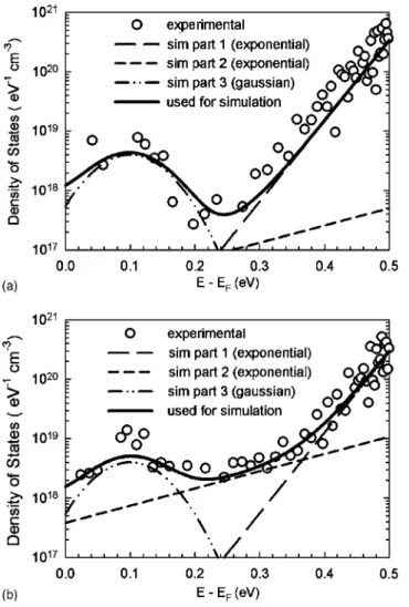
In contrast, since the hot-carrier degradation occurs near the drain side, the generated states can be treated as more uniformly distributed inside the D-MT. The DOS distribu-tions calculated from the subthreshold characteristics of the
D-MT shown in Fig. 2共b兲 before and after the hot-carrier stressing are shown in Figs.4共a兲and4共b兲, respectively. It can FIG. 1. Schematic and operating configurations of the test structure.
FIG. 2. Subthreshold characteristics of共a兲 TT and 共b兲 D-MT, before and after hot-carrier stressing under VG/ VD= 6.5 V / 13 V for 1000 s.
054508-2 Lee, Chang, and Lin J. Appl. Phys. 102, 054508共2007兲
be clearly and easily seen that the DOS increases after the stressing, especially in the range between 0.15 and 0.3 eV above the Fermi level.
This finding is very similar to the “type 2 of stress-created defects” proposed by Hack et al.24 They proposed that two types of defect are generated during the hot-carrier
stressing. “type 1” defects are generated when devices are stressed under linear conditions共VG⬎VD兲 and can be
mod-eled as an increase in DOS near the midgap. Type 2 defects, which are similar to what we found in this study, are gener-ated when devices are stressed in saturation 共VG⬍VD兲 and
can be modeled as an increase in DOS located 0.2– 0.3 eV above the Fermi level. They found that by adding type 2 defects in the region within 1m of the drain, the simulated subthreshold characteristics can match well with their experi-mental results. However, their conclusion is based on the simulated results which assume specific location of gener-ated defects. In contrast, we provide a direct evidence for the corresponding position within the band gap and the spatial location of such type of defect.
Temporal evolution of hot-carrier degradation at specific locations of the channel can also be addressed. Figure5 de-picts the evolution of subthreshold characteristics of D-MT during the hot-carrier stress of VG= 6.5 V and VD= 13 V. The
evolution of subthreshold characteristics in both logarithmic and linear scales are in agreement with the simulated results reported by Dimitriadis et al.,25 which suggest that this type of evolution is contributed by an increase in deep states. The evolution of extracted shift in subthreshold swing共⌬SS兲 for FIG. 3. Effective density-of-states distributions of TT before and after
hot-carrier stressing under VG/ VD= 6.5 V / 13 V for 1000 s.
FIG. 4. Effective density-of-states distributions of D-MT共a兲 before and 共b兲 after hot-carrier stressing under VG/ VD= 6.5 V / 13 V for 1000 s.
FIG. 5. Evolutions of subthreshold characteristics of D-MT in共a兲 logarith-mic and 共b兲 linear scales during hot-carrier stressing under VG/ VD = 6.5 V / 13 V.
FIG. 6. Evolutions of degradation in subthreshold swing of the test structure during hot-carrier stressing under VG/ VD= 6.5 V / 13 V.
all TT and MTs is shown in Fig. 6. It can be seen that al-though TT’s data show negligible subthreshold shift after the stressing, the D-MT shows unambiguous degradation at a very early stage, and the degradation increases monotoni-cally with increasing stress time.
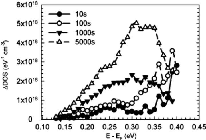
Using the aforementioned technique, the temporal evo-lution of DOS distribution of the degraded location, i.e.,
D-MT, during the hot-carrier stressing can also be observed.
Increase in DOS distributions of D-MT during hot-carrier
stressing is demonstrated in Fig.7. It appears that during the hot-carrier stressing, the DOS near the drain side continu-ously increases, especially for the states located 0.2– 0.4 eV above the Fermi level. The result demonstrates the capability of resolving the position of the generated states within the band gap.
Another tester was stressed under VG/ VD= 10 V / 20 V
for 1000 s. The subthreshold characteristics of all TT and MTs before and after the stressing were carefully measured. As shown in Figs. 8共a兲–8共d兲, the degradation in all transis-tors can be easily observed. Although the degradation can be observed on TT, MTs’ data provide a clearer picture, includ-ing not only better sensitivity enhancement but also the spa-tial location of two different types of degradation which oc-cur simultaneously. The degradation of the test transistor can be expressed as the combination of parallel shift in S-MT and degradations of subthreshold swing and on current in
D-MT. The mechanism of each phenomenon has been
intro-duced and discussed before.23
The DOS distributions for each MTs before and after the stressing are shown in Figs.9共a兲–9共c兲. The increase of DOS in Fig. 9共c兲 indicates that many defects are generated near the drain side during the stressing. Compared with the result of devices under minor stress conditions共shown in Fig.4兲, it
can be clearly seen that in addition to the increase between 0.15 and 0.3 eV above the Fermi level, significant increase FIG. 7. Increase in density-of-states distributions of D-MT during
hot-carrier stressing under VG/ VD= 6.5 V / 13 V.
FIG. 8. Subthreshold characteristics of 共a兲 TT, 共b兲 S-MT,共c兲 C-MT, and 共d兲 D-MT transistors in the test structure before and after the hot-carrier stressing under
VG/ VD= 10 V / 20 V for 1000 s.
054508-4 Lee, Chang, and Lin J. Appl. Phys. 102, 054508共2007兲
of tail states is also observed. It is reasonable since the chan-nel near the drain side is heavily damaged. The result also indicates that different types of defect are generated when the devices is stressed under minor or heavier conditions. In the experiments which employ traditional testers only, ex-trapolation from the result under heavier stress conditions is often used to predict the hot-carrier degradation under minor conditions. In this case, it appears that the direct observation using the MTs can provide more accurate information than
the commonly used extrapolation technique. For the S-MT, because the creation of positive charge located in the oxide23 affects the flatband voltage only, the DOS distribution in Fig.
9共a兲remains unchanged.
The extracted DOS distributions were also used for de-vice simulation to construct the I-V characteristics and vali-date the extracted results. One Gaussian and two exponential distributions were given to fit the DOS distribution used for simulation. For example, the extracted DOS distribution which was calculated from D-MT is shown by the circles in Fig.4. Three curves, marked as “sim part共1–3兲,” represent the corresponding distribution. It can be seen that the sum-mation of these three curves, which is represented by the solid line, matches well with the experimental results.
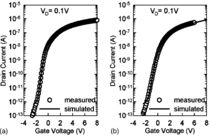
The DESSIS in ISE TCAD共Ref.26兲 was used to obtain
the simulated subthreshold characteristics. Figures10共a兲and
10共b兲 demonstrate the simulated I-V curves of D-MTs with the density-of-states distributions given from Figs.4共a兲and
4共b兲, respectively. The simulated data fit well with the mea-surement for both fresh and stressed samples. As mentioned before, the realistic density-of-states distributions after such nonuniform degradations are very difficult to obtain because of the limits of extraction technique. However, because the data extracted from monitor transistors can be employed to represent the localized defect distribution, the realistic distri-butions along the channel of TT can now be expressed be piecing together all MTs after the stressing. By giving the MTs’ data shown in Figs. 9共a兲–9共c兲, the channel of the TT can be split into three parts, as shown in Fig. 1. The DOS distribution of each part is then set using the data collected from the corresponding MT. Simulated subthreshold charac-teristics of the TT before and after the hot-carrier stressing using data collected from MTs are shown in Figs.11共a兲and
11共b兲, respectively.
CONCLUSIONS
In this work, a high-sensitivity TFT structure capable of spatially resolving hot-carrier degradation at a very early stage of stressing is employed to investigate the DOS char-acteristics. The nonuniform degradation along the channel could be clearly detected and characterized even under mild stress conditions. The effective DOS distributions in specific FIG. 9. Density-of-states distributions of 共a兲 S-MT, 共b兲 C-MT, and 共c兲
D-MT before and after hot-carrier stressing under VG/ VD= 10 V / 20 V for 1000 s.
FIG. 10. Simulated subthreshold characteristics of D-MT共a兲 before and 共b兲 after hot-carrier stressing under VG/ VD= 6.5 V / 13 V for 1000 s.
locations are extracted using field-effect conductance method. The effective DOS distributions reveal many useful and meaningful information not possible by traditional I-V characteristics. An increase in DOS is observed on certain position within the band gap when the device is stressed under mild conditions. Temporal evolution during the hot-carrier stressing is also characterized, and the monotonic in-crease in DOS distribution is observed. The extracted DOS distributions for both unstressed and stressed films are used to conduct a simulation for subthreshold characteristics of TFTs. The simulated I-V characteristics fitted well with the measured data. We have also simulated the subthreshold characteristics of the TTs before and after hot-carrier stress-ing usstress-ing the DOS distributions extracted from all MTs. The combination of the proposed test structure and DOS extrac-tion technique provides a powerful tool for resolving the nonuniform degradation of TFTs after hot-carrier stressing, which is difficult to achieve using traditional testers.
ACKNOWLEDGMENTS
The authors thank the staff of the National Nano Device Laboratory 共NDL兲 for their help in fabricating the test samples. They are also grateful to Professor Tiao-Yuan
Huang for helpful discussion. This work was supported in part by the National Science Council of the Republic of China under Contract No. NSC-95-2221-E-009-306.
1A. G. Lewis, I.-W. Wu, T. Y. Huang, A. Chiang, and R. H. Bruce, Tech.
Dig. - Int. Electron Devices Meet. 1990, 843.
2M. G. Clark, IEE Proc.: Circuits Devices Syst. 141, 3共1994兲. 3G. Fortunato, Thin Solid Films 296, 82共1997兲.
4S. H. Jung, W. J. Nam, J. H. Lee, J. H. Jeon, and M. K. Han, IEEE
Electron Device Lett. 26, 23共2005兲.
5Y. Uraoka, T. Hatayama, T. Fuyuki, T. Kawamura, and Y. Tsuchihashi,
IEEE Trans. Electron Devices ED-48, 2370共2001兲.
6Y. Jeong, D. Nagashima, H. Kuwano, T. Nouda, and H. Hamada, Jpn. J.
Appl. Phys., Part 1 41, 5042共2002兲.
7B. Doyle, M. Bourcerie, J.-C. Marchetaux, and A. Boudou, IEEE Trans.
Electron Devices ED-37, 744共1990兲.
8T. Yoshida, K. Yoshino, M. Takei, A. Hara, N. Sasaki, and T. Tsuchiya,
Tech. Dig. - Int. Electron Devices Meet. 2003, 8.8.1.
9T.-F. Chen, C.-F. Yeh, and J.-C. Lou, J. Appl. Phys. 95, 5788共2004兲. 10K. C. Moon, J.-H. Lee, and M.-K. Han, IEEE Trans. Electron Devices
ED-52, 512共2005兲.
11Y. Uraoka, T. Hatayama, T. Fuyuki, T. Kawamura, and Y. Tsuchhashi,
2001 International Conference on Microelectronic Test Structures, Vol. 14,
p. 251共2001兲兴.
12A. T. Hatzopoulos, D. H. Tassis, N. A. Hastas, C. A. Dimitriadis, and G.
Kamarinos, IEEE Trans. Electron Devices ED-52, 2182共2005兲.
13Y. Uraoka, N. Hirai, H. Yano, T. Hatayama, and T. Fuyuki, Tech. Dig.
-Int. Electron Devices Meet. 2002, 577.
14W. B. Jackson, N. M. Johnson, and D. K. Biegelsen, Appl. Phys. Lett. 43,
195共1983兲.
15B. Faughnan, Appl. Phys. Lett. 50, 290共1987兲.
16M. Cao, T. J. King, and K. C. Saraswat, Appl. Phys. Lett. 61, 672共1992兲. 17T. J. King, M. G. Hack, and I. W. Wu, J. Appl. Phys. 75, 908共1994兲. 18H.-C. Lin, M.-H. Lee, and K.-H. Chang, IEEE Electron Device Lett. 27,
561共2006兲.
19G. Fortunato and P. Migliorato, Philos. Mag. B 57, 573共1988兲. 20T. Suzuki, Y. Osaka, and M. Hirose, Jpn. J. Appl. Phys., Part 2 21, L169
共1982兲.
21G. Fortunato and P. Migliorato, Appl. Phys. Lett. 49, 1025共1986兲. 22G. Fortunato, D. B. Meakin, P. Migliorato, and P. G. Le Comber, Philos.
Mag. B 57, 573共1988兲.
23M. H. Lee, K. H. Chang, and H. C. Lin, J. Appl. Phys. 101, 054518
共2007兲.
24M. Hack and A. G. Lewis, IEEE Trans. Electron Devices ED-40, 890
共1993兲.
25C. A. Dimitriadis, M. Kimura, M. Miyasaka, S. Inoue, F. V. Farmakis, J.
Brini, and G. Kamarinos, Solid-State Electron. 44, 2025共2000兲.
26More information of ISE TCAD can be seen on Synopsys’ web: http://
www.synopsys.com/products/tcad/tcad.html FIG. 11. Simulated subthreshold characteristics using data collected from
MTs.
054508-6 Lee, Chang, and Lin J. Appl. Phys. 102, 054508共2007兲