Edge Hole Direct Tunneling in Off-State Ultrathin Gate Oxide p-Channel MOSFETs
K.
N.
Yang, H.
T. Huang,
M. J. Chen, Y. M. Lin*, M. C.
Yu*,
S.
M. Jang*, C. H.
Yu*,
M.
S.
Liang*
Department of Electronics Engineering, National Chiao-Tung University, Hsin-Chu, Taiwan, ROC *R/D Department, Taiwan Semiconductor Manufacturing Company, Hsin-Chu, Taiwan, ROC
Abstract
This paper examines the edge direct tunneling (EDT) of hole from p+ polysilicon to underlying p-type drain extension in off- state p-channel MOSFETs having ultrathin gate oxide thicknesses (1.2
-
2.2 nm). It is found that for thinner oxide thicknesses, hole EDT is more pronounced over the conventional GIDL and gate-to-channel tunneling, and as a result, the induced gate and drain leakage is better measured per unit gate width. A physical model accounting for heavy and light hole's subbands in the quantized accumulation polysilicon surface is built explicitly. This model consistently reproduces EDT I-V and the tunneling path size extracted falls adequately within the gate-to-drain overlap region. The ultimate oxide thickness limit due to EDT is projected as well.Introduction
The scaled gate oxide thickness is now approaching the direct tunneling regime [I]. The gate leakage due to direct tunneling [2] was usually measured per unit oxide area [3],[4], and a certain criterion of 1 A/cmz set the ultimate limit of scalable oxide thicknesses [3],[4]. For n-channel devices operated in off state, the edge direct tunneling (EDT) [ 5 ] , [ 6 ] of electron from n+ polysilicon to underlying drain extension not only dominates the gate leakage, but also can prevail over the conventional GlDL. This paper explores straightforward the EDT of hole from p'polysilicon to p-type drain extension in p- channel counterpart. It is clarified that the induced gate and drain leakage indeed originates from the edge part rather than the whole gate oxide, and thus is better measured per unit gate
width. Also presented is a physical model enabling consistently the reproduction of EDT I-V, the extraction of EDT path size, and the projection of ultimate oxide thickness.
Experiment and Characterization
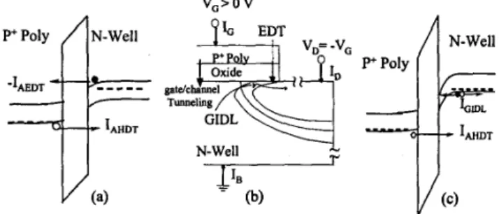
Test pattems including p+ poly-gate p-channel MOSFETs and CMOS inverters were fabricated by a 0.18-um process technology [7]. The gate oxides were grown in diluted wet oxygen ambient to three different physical thicknesses T, of 1.23, 1.85, and 2.16 nm. These values for p-channel devices were extracted by citing an electron direct tunneling I-V model [8] and were all confirmed by high resolution TEM and a C-V method accounting for polysilicon depletion and Quantum Mechanical effects, as detailed elsewhere [9]. Fig. 1 illustrates three plausible tunneling leakage paths for off-state p-channel MOSFETs and related band diagrams.
EDT
v,=
-v,
gaWchanoel Tunneling N-Well N-Well P+ PolyFig. 1 (a) Band diagram located at channel region far from LDD. Accumulation hole direct tunneling current (IAHDT) and electron direct tunneling (IAEM) both contribute to gatelchannel tunneling. (b) Schematic cross section near gatddrain overlap region under V G a V and VD= -VG. Three tunneling current paths are shown. (c) Band diagram located at gatddrain overlap region, showing hole EDT and GIDL.
With source open and under V, = -V,, the measured drain current ID, gate current I,, and bulk current IB are plotted in Fig. 2 versus VGD for three different oxide thicknesses. Fig. 2(a) and
(b) reveal that the drain current primarily comprises the GlDL and the gate current, favoring EDT as the origin of the latter component. It is seen that a certain range of V,D exists where the EDT prevails over the GIDL, and such range is expanded for decreased Tox. We attribute the EDT herein via hole rather than valence electron tunneling. This can be evidenced based on the band diagram in Fig. 1 that for low voltage V,, it is essentially improbable for valence electron tunneling across the oxide to the forbidden gap in polysilicon side. In Fig. 2(c) for T, = 1.23
nm,
the gate-to-channel tunneling constitutes solely the bulk current making GIDL impossible to detect. Note that hole EDT dominates the gate current for allTax.
29.6.1
' O " 8 0.5 I 1.5 2 2.5 3 3.5 4
VGD (VI (c)
Fig.2 Measured terminal currents versus VGD for three different To, (a), @), and (c) under VD= -VG and source open. The aspect ratio W b I O w0.5 p. (a) Hole EDT dominates the drain leakage
b
in 0 V<VaD<2.3 V. @) Hole EDT dominates b in 0 VcVOD<2.6 V and GIDL constitutes drain leakage for V G a 2 . 6 V. (c) The edge tunneling mechanism prevails over almost the drain leakage current.With source grounded and V, =-1.8 V, the measured terminal currents versus both polarities of V, are plotted in Fig. 3. Obviously, the GIDL dominates the drain leakage for To, =
2.16
nm,
while for thinner To, of 1.85 nm such role is replaced by hole EDT in 0 V <VG
< 0.9 V, and eventually is entirely controlled by hole EDT for To, = 1.23nm.
Fig. 3(c) shows the bulk current reversal phenomena due to two opposite sources: GIDL and gate-to-channel tunneling. Regarding on-state I-V (negativeV,)
in Fig. 3, the impact of hole direct tunneling from the inverted channel in degrading drive capability is described inour
recentwork
191.Fig. 3 Measured terminal current versus both polarities of gate aspect ratio WL-10 p d O . 5 p. Source grounded and VD=1.8 V.
We also found experimentally that the hole EDT indeed proportional to the gate width, regardless of
voltage. The
leakage is the aspect ratio
(WL).
This means that the induced gate and drain leakage is better measured per unit gate width. Fig. 4 displays the supply current and input current all versus input voltage V, measured onCMOS
inverter withTo,
= 1.23 nm for different supply voltage VDD. It can be observed that (i) at high-level state V, = V,, the standby current comes from the hole EDT of off-state p- channel device and the electron direct tunneling fiom inverted channel in turn-on n-channel one; and (ii) at low-level state V, = 0, the standby current comprises the electron EDT [5],[6] ofoff-
state n-channel and the hole direct tunneling from inverted channel in on-state p-channel [9]. Attached in Fig. 4 is the measured ratio of each component. It is expected that as channel length continues to shrink, the role ofEDT
substantially increases since source/drain extension does not easily scale[51,[111.
29.6.2
Triangular
-
Potenfial Approximation n5
10.' cB
5
10-5 U 10.' I 0''Fig. 4 (a) Measurement set-up for two standby modes and (b) measured supply currents, IDD and Iss, and input current, IIN, versus input voltage VIN from an inverter with T o ~ l . 2 3 nm for different supply voltage VDD Gate leakage paths in two standby modes are shown. The gate length is 0.18 p.
Hole EDT Modeling
By following a published analytic electron direct tunneling model [8], a hole EDT version was built:
where
&(=bp
xW) is the effective tunneling path cross- section area;bp
is the tunneling path size; Q is sheet charge of the accumulation layer;f
is hole impact frequency on the p*- poly/SiO, interface; and T is the modified WKB transmission probability including interface reflection correction. The oxide field E,, at the gate edge is one key input parameter to the model.I,, =A,Q f T = L,WQ f T
L E ,
r(l
P-Typc LDD(Dccp.Depl#~on Approx.)
Fig. 5 Band diagram drawn along P+-Polysilicon/Oxide/LDD. The
accumulation potential bending, ,,,V with 2DHG(Z-DimensionaI Hole Gas) Concept and the silicon surface potential, VLDD, with the deep depletion approximation are adopted in the procedure of Eox extraction.
Applying the first subband approximation to
the
accumulated pt poly gate and the deep depletion approximation to the underlying LDD region as shown in Fig. 5 , we can get a simplified form to facilitate the extraction of E, as shown below:
.. ..
First
-
Subband ApproximationE ox Ea = [ ~ ~ L z H ( ~ F
-
g20L(EF-
E L l ) l q +Deep
-
Depletion ApproximationNote that the index H means heavy hole and L means light hole. g, represents two dimensional density of state and E, means the ground energy of triangle-like potential. For <loo> poly grain orientation, mH,=0.29 m,,, mH,,,=0.433 q; mL,=0.20
m,,, m,,,,=O. 169 m,, as all cited in [lo].
Once E, was quantified, an excellent reproduction was achieved with LDD dopant NLDD=8x10'8 l/cm3 and effective mass qfi =0.38 m, for both heavy and light hole resulting from parabolic dispersion relation in tunneling oxide, as depicted in Fig. 6 . The tunneling path size extracted was 6 nm wide
(=bp)
from the gate edge (since NLDD quite matches the highly-doped one). This is reasonable since the drain extension beneath the gate is about 8 nm.
0 1 2 3 4 5 6
1u
Eox (MV/cm)
Fig. 6 Comparison of the calculated and experimental hole EDT current versus Eo% The extracted effective EDT range is 6 MI wide from the gate edge.
w=10
m.
29.6.3
7
---
'y.1
Current L i m i t-.
Feature Size (pii)
Fig. 7 (a) Showing the location of the edge hole direct tunneling. @) The calculated hole direct tunneling per gate width versus scaling generation oxide thickness in PMOSFETs. V , , (V) To, (um) 0.13 I I 0.10
I
1.2I
1.8It is recognized [5],[11] that drain extension may be considered a non-scalable factor, implying a constant
bp
of 6 nm in the scaling direction.v,= .VDD 0 NhlOSPETs 0.25 pan 10 20 30 4 0 50 60 Tox (A) (b)
Fig. 8 (a) Showing the location of the edge electron direct tunneling in NMOSFETs. (b) The calculated electron direct tunneling per gate width versus scaling generation oxide thickness. Effective tunneling path is 6.25 nm wide from the gate edge [6].
With this in mind, the conventional criterion of 1 Ncm' can be transferred to 0.6 CIA/cm. Using the roadmap parameters [ 11, the hole EDT current is calculated versus scaling generation oxide thickness as shown in Fig. 7. In Fig. 7 the new criterion due to hole EDT sets the ultimate oxide thickness of around 1.42 nm. Similarly, the electron EDT current for off-state n-channel device is calculated [6] versus scaling generation oxide thickness as shown in Fig. 8 for reference. The tunneling path size extracted was 6.25 nm wide from the gate edge [6].
Conclusion
The edge direct tunneling (EDT) of hole from p+ polysilicon to underlying p-type drain extension has shown its tremendous impact
on
the drain leakage and gate leakage. A physical model has been built and has reproduced consistently experimental EDT I-V characteristics. The tunneling area extracted has been found to fall within the gate-to-drain overlap region. The ultimate oxide thickness due to hole EDT has also been projected based on the model.Acknowledgment
The work was supported by the National Science Council under Contract No. NSC 88-22 IS-E-009-047.
References
[I] Intemational Technology Roadmap for Semiconductors, 1999 Edition. [2] H. S. Momose et al., IEEE Truns. EIecrmn Devices, vol. 43, p.1233,
1996.
[3] S . H. Lo et al., IEEE Electmn Device Leff., vol. 18, p.209, 1997. [4] G. Timp et al., IEDMTech. Dig., p. 615, 1998.
[ 5 ] N. Yang et al., IEDM Tech. Dig., p. 453,1999.
[6] K. N. Yang et al., SSDM 2000 (accepted).
[7] C. H. D i u et al., Dig. Symp. V U 1 Technol., p. 11, 1999. [8] L. F. Register et al., Appl. Phys. Letf., vol. 74, p. 457,1999. [9] K. N. Yang et al., IEEE Trans. Electron Devices, 2000 (accepted). [lo] S. Takagi et al., IEEE Truns. Elecrmn Devices, vol. 46, p.1446, 1999.
[ I I] S . Thompson et al., Dig. Symp. YLSI Technol.. p.132, 1998.