國 立 交 通 大 學
電信工程學系
碩 士 論 文
Ku 頻段反射式類比移相器
與縮小化寬頻阻抗轉換微波岔路環
Ku Band Reflection-Type Analog Phase Shifter and
Reduced-size Broadband Impedance-Transforming
180
oHybrid Ring Coupler
研究生:陳威綸
指導教授:張志揚 博士
Ku 頻段反射式類比移相器
與縮小化寬頻阻抗轉換微波岔路環
Ku Band Reflection-Type Analog Phase Shifter and
Reduced-size Broadband Impedance-Transforming
180
oHybrid Ring Coupler
研 究 生:陳威綸
Student:Wei-Lun Chen
指導教授:張志揚 博士 Advisor:Dr. Chi-Yang Chang
國立交通大學
電信工程學系
碩士論文
A Thesis
Submitted to Department of Communication Engineering
College of Electrical and Computer Engineering
National Chiao Tung University
In Partial Fulfillment of the Requirements
for the Degree of
Master of Science
In
Communication Engineering
June 2008
Hsinchu, Taiwan, Republic of China
中華民國 九十七 年 六 月
Ku 頻段反射式類比移相器
與縮小化寬頻阻抗轉換微波岔路環
研究生:陳威綸 指導教授:張志揚 博士
國立交通大學電信工程學系
摘要
本論文前半部提出兩種適用於
Ku 頻帶的類比反射式移相器:
一種是將可變電容二極體諧振並轉換阻抗使可移轉角度增加到
280
度,另一種是透過並聯兩個可變電容二極體的方式使可移轉角度超
過
360 度。並且,本文利用此移相器設計了一個可調整天線主波束
方向的相位陣列。
本論文後半部份設計一個中心頻率為
3GHz 的寬頻微波岔路
環。在各輸出入埠加上額外的單位元件(unit element 即為一段四分
之一波長傳輸線),可使頻寬接近 100%並具有阻抗轉換功能(40 歐
姆到
120 歐姆)。結構上,利用歩階阻抗共平面帶線可以得到理想的
反相器、壓制高頻諧波、和使體積縮小為原來的
70%等優點。
Ku Band Reflection-Type Analog Phase
Shifter and Reduced-size Broadband Impedance-
Transforming 180
oHybrid Ring Coupler
Student: Wei-Lun Chen Advisor: Dr. Chi-Yang Chang
Department of Communication Engineering
National Chiao-Tung University
Abstract
In the first part, we propose two Ku band reflection-type phase shifters using four and two varactors to exhibit maximum phase shift of 360o and 286o, respectively. For a single varactor, the maximum phase shift is increased by resonating the varactor and impedance transforming at the input of the reflection load. The 360o phase shift results from the parallel connection of two series tuned varactors. A 4-element phased array is designed and fabricated to verify the phase shifter.
In the second part, the 180o hybrid ring adding a unit element at each port has been designed to exhibit Chebyshev response and impedance transformation. We use hybrid CPS/interdigital CPS as stepped-impedance and ideal phase inverter for size reduction of 70% and wideband performance. The fabricated 180o hybrid ring exhibits a wide bandwidth of almost 100%, and its amplitude and phase balance are less than 0.55dB and 4o, respectively. For system impedance transformation of 40Ω and 120Ω, each port of the proposed 180o hybrid ring is well-matched.
Acknowledgement
誌 謝
經過兩年的研究所生涯,終於完成了這本碩士論文。本篇論文與
研究所課業得以完成,最要感謝的就是我的指導教授張志揚博士。兩
年來,老師的細心教誨幫助我克服了許多研究上的難題。除此之外,
老師在我的人生啟蒙上也給予了許多指導,在此由衷的感謝老師。同
時感謝口試委員鍾世忠教授、邱煥凱教授與陳正中博士提供的寶貴意
見,使本論文更加完善。
感謝實驗室博士班學長慧諄、金雄、鈞翔、哲慶、建育與正憲的
指導,尤其是哲慶學長毫不保留的將經驗與知識傳授給我,對我的論
文研究有非常大幫助,並且也感謝其他實驗室學長的幫忙。感謝實驗
室同窗逸銘、智皓、人錞、獻文與逸亭在學業與生活上的陪伴與照顧,
讓我能在充滿歡樂氣氛的實驗室下進行研究與學習。另外,也感謝求
學過程中一路陪伴我的好友們,謝謝你們的支持與鼓勵。
最後要感謝一直支持我的家人們:爸爸、媽媽和姊姊。有你們的
支持,讓我的求學過程十分順利,使我無後顧之憂的完成碩士學位。
Table of Contents
Abstract (Chinese) ... i
Abstract ... iii
Acknowledgement ...v
Table of Contents ... vii
List of Tables... xi
List of Figures ... xiii
Chapter 1 Introduction... 1
1.1 Ku Band Reflection-Type Phase Shifter ... 1
1.2 Reduced-Size Impedance-Transforming Broadband 180o Hybrid Ring ... 3
Chapter 2 360o Reflection-Type Analog Phase Shifter... 5
2.1 Introduction... 5
2.2 Design Procedure ... 8
2.2.1 Reflection-Type Phase Shifter ... 8
2.2.2 Series Resonant Varactor... 9
2.2.3 Parallel Resonant Load ... 13
2.2.4 Changing Port Impedance of Reflection Loads ... 16
2.3 Simulation Results ... 17
2.4 Fabrication and Measurements ... 20
2.4.1 Performance against control voltage... 20
2.4.2 Performance against frequency ... 23
3.1 Introduction... 25
3.2 Theory of Reflection-Type Phase Shifter... 26
3.2.1 Analysis... 27
3.2.2 Design Formula... 28
3.3 Design Procedure of Ku Band Phase Shifter ... 30
3.3.1 Series Resonant Varactor... 31
3.3.2 Changing Port Impedance of Reflection Loads ... 31
3.3.3 Compensation for Insertion-Loss Variation ... 36
3.4 Fabrication and Measurements of Ku Band Phase Shifter ... 38
3.4.1 Performance against control voltage... 39
3.4.2 Performance against frequency ... 42
3.5 Ku Band Phased Array... 44
3.5.1 Theory ... 44
3.5.2 Design ... 47
3.5.3 Fabrication and Measurements ... 47
Chapter 4 Reduced-Size Impedance-Transforming Broadband 180o Hybrid Ring ... 51
4.1 Introduction... 51
4.2 Theory ... 54
4.2.1 Conventional 180o Hybrid Ring... 54
4.2.2 Impedance-Transforming Broadband 180o Hybrid Ring ... 56
4.2.3 Cost Function and Optimization ... 60
4.2.4 Stepped-Impedance Structure ... 63
4.2.5 Hybrid CPS/Interdigital CPS Structure... 65
4.3.1 Design Procedure ... 67
4.3.2 EM Simulation ... 67
4.4 Fabrication and Measurements ... 71
Chapter 5 Conclusion ... 77
List of Tables
Table 2.1: Measured phase of reflection coefficient of varactors at 12.45 GHz...12 Table 2.2: Measured resistance of the resonant varactor against bias voltage...12 Table 2.3: Physical dimensions of the proposed 360o reflection-type phase shifter.18 Table 4.1: Parameters of the proposed 180o hybrid ring...64 Table 4.2: Parameters of the hybrid CPS/interdigital CPS ...65 Table 4.3: Parameters and physical dimensions of the proposed stepped-impedance
List of Figures
Figure 2.1: Different approaches for reflection loads of the 360o phase shifter. (a) Dual varactor termination for doubling phase shift range [3]. (b) Tunable short-terminated combline filter [4]. (c) In-series cascaded connection of varactors with the impedance-transforming quadrature coupler [5]. (d)
Ladder-type reflection loads [6]...7
Figure 2.2: Circuit schematic of the proposed 360o reflection-type phase shifter...8
Figure 2.3: Generic reflection-type phase shifter ...9
Figure 2.4: The circuit model of MA-COM MA46H120 varactor...9
Figure 2.5: Two ground structures of termination loads. (a) Layout of the load with RF virtual ground. (b) Equivalent circuit of the load with RF virtual ground. (c) Layout of series resonant loads (d) Equivalent circuit of series resonant varactor...10
Figure 2.6: The reflection coefficient of the resonant varactor on the Smith Chart ....13
Figure 2.7: Two series resonant varactor forming a parallel resonant circuit using (a) lump elements (b) transmission lines...14
Figure 2.8: Two series resonant varactor forming a parallel resonant circuit. (a) Two series resonant varactor. (b) Parallel resonant circuit. (c) Modified parallel circuit. ...15
Figure 2.9: Two cascaded quarter-wave impedance transformers ...17
Figure 2.10: The circuit layout of the proposed 360o reflection-type phase shifter...18
Figure 2.11: Simulated relative phase shift and insertion loss of the proposed 360o phase shifter at 12.45GHz...19
Figure 2.13: Photograph of the proposed 360o reflection-type phase shifter ...20 Figure 2.14: Measured results of the proposed 360o phase shifter against control
voltage at 12.45GHz. (a) Relative phase shift. (b) Insertion loss. (c) S21
on Smith Chart. ...21 Figure 2.15: Comparison of relative phase shift between the proposed 360o phase
shifter, series resonant varactor, and a single varactor...22 Figure 2.16: Frequency response of the 360o phase shifter. (a) Relative phase shift.
(b) Insertion loss. (c) Return loss...23 Figure 3.1: Circuit model of reflection loads (a) Varactor. (b) Series resonant
varactor. (c) Series resonant loads with compensating resistance ...28 Figure 3.2: (a) Varactor load with a transmission line with L1=6o. (b) Reflection
coefficient on the Smith Chart. ...32 Figure 3.3: Reflection coefficient of reflection loads at 12.45 GHz. (a) Z0=25Ω,
maximum phase shift = 195o. Insertion loss variation = 1.4dB. (b)
Z0=13Ω, maximum phase shift = 266o. Insertion loss variation =
2.8.dB...33 Figure 3.4: (a) Maximum phase shift and (b) Insertion loss variation against port
impedance Z0 ...33
Figure 3.5: Reflection load with two cascaded impedance transformers. Z1=118Ω,
Z0=50Ω, L1=6o ...34
Figure 3.6: Comparison of phase shift of the reflection load with and without impedance transformers. ...35 Figure 3.7: Reflection load with compensating resistance RP. Z1=118Ω, Z0=50Ω,
L1=6o, R =200Ω...36
GHz. (a) Relative phase shift and (b) Return loss of the reflection load against bias voltage of varactor...37 Figure 3.10: Photograph of the proposed phase shifter circuits (a) without RP (b)
with RP=220Ω ...39
Figure 3.11: Measured results of the proposed phase shifters against bias voltage at 12.45 GHz. (a) Relative phase shift. (b) Insertion loss...40 Figure 3.12: Measured S21 of the proposed phase shifters at 12.45 GHz ...41
Figure 3.13: Measured frequency performance of the proposed phase shift. (a) Insertion loss. (b) Return loss. (c) Relative phase shift. ...42 Figure 3.14: Phased array composed of N antennas with equidistance...45 Figure 3.15: Simulated radiation pattern of 4-element phased array...46 Figure 3.16: Relationship between the angle of main beam and phase shift between
successive antennas...46 Figure 3.17: The structure of the proposed phased array. (RTPS: reflection-type
phase shifter. LNA: low noise amplifier) ...47 Figure 3.18: Photograph of the proposed phased array. (a) Dipole antenna. (b)
Directional coupler. (c) Reflection-type phase shifter. (d) Low noise amplifier. (e) Chip resistor (100Ω). (f) Control voltage of phase shifters (0-10V). (g) LNA bias voltage (1.5V) ...48 Figure 3.19: Measured radiation pattern of the proposed Ku band phased array at (a)
12.2 GHz. (b) 12.45 GHz. (c) 12.7 GHz...50 Figure 3.20: The angle of main beam against control voltage...50 Figure 4.1: Circuit schematics of 180o hybrid ring with an ideal phase inverter. (a)
Conventional 180o hybrid ring. (b) Proposed broadband 180o hybrid ring with different impedance at input and output ports...53 Figure 4.2: (b) Even- and (b) Odd-mode equivalent circuits of the 180o hybrid ring
with an ideal phase inverter ...54 Figure 4.3: Circuit schematics of (a) the reconfigured hybrid ring with an ideal
phase inverter (b) one pair of unit elements with the same impedance at the same side ...57 Figure 4.4: Simulated frequency response of the proposed impedance-transforming
broadband 180o hybrid ring ...62 Figure 4.5: Stepped-impedance structure equivalent to a λ/4 transmission line...63 Figure 4.6: Simulated frequency response of the proposed stepped-impedance
impedance-transforming broadband 180o hybrid ring using ideal transmission lines...64 Figure 4.7: The cross section view of the interdigital CPS structure proposed in [21] ...
...65 Figure 4.8: The layouts of the λ/4 line section using hybrid CPS/interdigital CPS
structure proposed in [21] (a) λ/4 line section. (b) λ/4 line section with an 180o phase inverter. ...66 Figure 4.9: The circuit layout of the proposed stepped-impedance impedance-
transforming broadband 180o hybrid ring. (a) Total circuit. (b) λ/4 line section using hybrid CPS/interdigital CPS ...68 Figure 4.10: The simulated results of return loss and coupling of the proposed
impedance-transforming broadband 180o hybrid ring. (a) Out-of-phase operation. (b) In-phase operation...70 Figure 4.11: Simulated return loss for all the ports of the proposed impedance-
transforming broadband 180o hybrid ring...71 Figure 4.12: Simulated broadband performance of the proposed 180o hybrid ring...71 Figure 4.13: Measured and Simulated results of the proposed impedance-
(b) In-phase operation...72 Figure 4.14: Measured amplitude and phase balance of the proposed impedance-
transforming broadband 180o hybrid ring. (a) Out-of-phase operation. (b) In-phase operation...73 Figure 4.15: Measured and simulated results of return loss for all the ports of the
proposed impedance-transforming broadband 180o hybrid ring. ...75 Figure 4.16: Measured broadband performance of the proposed impedance-
transforming broadband 180o hybrid ring...75 Figure 4.17: Photograph of the proposed impedance-transforming broadband 180o
Chapter 1
Introduction
1.1
Ku band Reflection-Type Phase Shifter
The Ku band (K-under band), of which the range of frequency is 11.7-12.7 GHz for downlink and 14-14.5 GHz for uplink, is primarily used for satellite communications, especially for editing and broadcasting satellite television. The 12.2 to 12.7 GHz segment is allocated to the broadcasting satellite service (BSS). Typically, satellite television systems transmit and receive signals by antenna systems with high directivity, such as satellite dish antennas. Besides the high directivity, if a receiver of the satellite television is employed on a vehicle, an antenna system requires adaptive beamforming in order to tracking the satellite when the vehicle moving uphill and downhill. The phased array is therefore useful for beamforming in the mobile satellite television system.
Phase shifters are necessary components in a phased-array antenna system. Design of phase shifters requires consideration of many factors such as large phase shift, low insertion loss, low phase error, bandwidth, low insertion-loss variation, simple control, low dc power consumption, and low cost for commercial wireless communication. In
this study, we propose two configurations of Ku band reflection-type phase shifters, in which four and two varactors are used, respectively.
In chapter two, a Ku band reflection-type analog phase shifter with 360o phase shift
is proposed. The basic circuit of the phase shifter comprises a 3-dB 90o hybrid
coupler terminated with two identical reflection loads. In order to achieve 360o phase
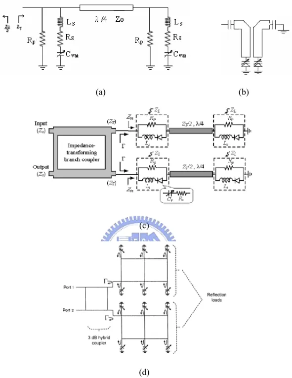
shift range, the reflection load is made of the parallel connection of two series tuned varactors so that there are four varactors in a phase shifter. The proposed phase shifter is designed with excellent match and linear voltage-phase relationship
In chapter three, we propose a Ku band phased array with beam steering by changing the phase between antenna elements using reflection-type analog phase shifter. Instead of using four varactors in the phase shifter proposed in chapter two, we use two varactors in this phase shifter at the cost of less phase shift. The reflection load can’t achieve a phase shift of 360o by a single varactor. This work extends the
maximum phase shift, which was originally limited by the capacitance tuning range of the varactor, from 52o to 286o by resonating the varactor with via inductance and
using λ/4 impedance transformers between the branch line coupler and the varactor. Finally, the proposed phase shifters are integrated to a 4-element phased array for beam steering. Design procedure and measurement results will be showed.
1.2
Reduced-Size Impedance-Transforming
Broadband 180
oHybrid Ring
The 180o hybrid ring coupler, which is also known as the rat-race ring, is an
essential component in microwave circuits, such as balanced mixers, multipliers, push-pull amplifiers and antenna feed network, etc. In chapter four, a reduced-sized impedance-transforming broadband 180o hybrid ring coupler is proposed. With a unit
element at each port and an ideal phase inverter, the broadband 180o hybrid ring with
impedance transformation between the input and output ports is proposed. After formulating the scattering matrix of the 180o hybrid ring, the values of circuit
parameters are derived by the optimization method to fit the 180o hybrid ring to a
Chebyshev response. We replace each line section by three sections of stepped impedance transmission lines using CPS/interdigital CPS structure to realize an ideal 180 o phase inverter and to reduce the length of each line section. The circuit analysis,
Chapter 2
360
o
Reflection-Type Phase Shifter
2.1 Introduction
Reflection-type phase shifters have many advantages such as good matching, low insertion loss, simple control, and low DC power consumption, so it is popular in phase shifter design. Using active components such as varactor diodes as reflection loads was first introduced in [1]. Varactors are commonly used as reflection loads so that the phase shift is limited to the capacitance tuning range of the varactor. The maximum phase shift can be extended by resonating the varactor with an inductance or changing the port impedance of the reflection load. But even when these methods are utilized, it is difficult to achieve a phase shift of 360o by a single varactor.
In order to get 360o phase shift range, several approaches have been proposed. The
most popular approach is to cascade two series resonant varactors with a quarter- wavelength transmission line [2] [3], which is shown in Figure 2.1(a). For the dual varactor termination, the phase shift range of the reflection load is doubled. In [4] (Figure 2.1(b)), it is shown that using tunable short-terminated combline filters as reflection load also provide double insertion phase. Another approach is the
combination of two series connected varactors separated by a quarter-wave transmission line and an impedance-transforming quadrature coupler [5] (Figure 2.1(c)). The required varactor capacitance variation is smaller if the impedance ratio of the impedance-transforming quadrature coupler is enlarged. Instead of the resonant load, a ladder-type reflection type phase shifter with six varactors and seven quarter-wave transmission shown in Figure 2.1(d) is proposed [6]. The total phase shift is the sum of the tunable phase of each varactor, so it can achieve large phase shift without inductors.
In addition to all of the above, using two different series tuned varactors in a parallel connection to achieve 360o phase shift was provided by B. T. Henoch and P.
Tamm [7]. The author obtained a 360o phase shifter which has minimum variation of
total phase shift versus frequency. In [8], the original varactor impedance was transformed by the transmission line, and linear voltage-phase relationship is obtained. In this chapter, we propose a full 360o phase shifter with the reflection load using two
resonating loads in a parallel configuration, so there are four varactors in total. The circuit schematic is shown in Figure 2.2. The proposed phase shifter is designed with excellent match and linear voltage-phase relationship at Ku band, where parasitic effects of all components such as resistors and varactor diodes have to be considered. Detail design procedure and measurement results will be discussed.
(a) (b)
(c)
(d)
Figure 2.1: Different approaches for reflection loads of the 360o phase shifter. (a)
Dual varactor termination for doubling phase shift range [3]. (b) Tunable short-terminated combline filter [4]. (c) In-series cascaded connection of varactors with the impedance-transforming quadrature coupler [5]. (d) Ladder-type reflection loads [6].
Figure 2.2: Circuit schematic of the proposed 360o reflection-type phase shifter.
2.2 Design Procedure
2.2.1 Reflection-Type
Phase
Shifter
As shown in Figure 2.3, a generic reflection-type phase shifter is composed of a 3-dB 90o hybrid coupler and two identical reflection loads. Due to the 3-dB hybrid 90o
coupler, input signal is equally divided by the coupler in quadrature phase. The phase of reflected signal is determined by the reflection coefficient of the reflection load. Because the reflection loads are identical, two reflected signals are combined in-phase at output port. On the other hand, two reflected signals are cancelled out each other at input port. Thus, the phase shift provided by the phase shifter is equal to the phase shift of the reflection load.
Figure 2.3: Generic reflection-type phase shifter
2.2.2 Series
Resonant
Varactor
The proposed phase shifter is designed at the center frequency of 12.45 GHz. MA-COM MA46H120, which is a gallium arsenide flip chip varactor diode, is used as the termination loads of the phase shifter. The circuit model is shown in Figure 2.4, where LS, RS, and CP are the series inductance, series resistance, and package
capacitance of the varactor diode. The tuning range of varactor capacitance CJ is from
0.2pF to 1pF. However, suffering form parasitic effects of LS, RS, and CP, the
characteristic of the varactor is not simply a capacitance at high frequency. Thus, the first step is to measure the characteristics of the varactor.
Figure 2.5 shows two different ground structures the varactor diode mounted. The gray lines represent the microstrip line. Via holes connect the top metal to the bottom, which is a metallic ground plane. The varactor is mounted between the microstrip line and the ground area, and its reverse bias voltage is applied on the left side.
(a) (b)
(c) (d) Figure 2.5: Two ground structures of termination loads.
(a) Layout of the load with RF virtual ground.
(b) Equivalent circuit of the load with RF virtual ground. (c) Layout of series resonant loads
Figure 2.5(a) shows that the top view of the ground structure, composed of a shunt connection of a fan stub and a quarter-wave short stub, is a RF virtual ground and DC return. A fan stub can achieve a “perfect short” over a moderate bandwidth. On the other hand, the short stub using via holes acts like a “perfect open” for RF signals, so there is no via hole effect. Thus, we can derive the characteristics of the varactor by measuring the reflection coefficient. Figure 2.5(b) shows its equivalent circuit. Measured equivalent reactance varies from -23Ω to -61Ω with tunable reactance ratio of 2.7 and total phase shift of 52o at the bias voltage range of 0V to 10V. Parasitic
resistance varies from 3Ω(V=0V) to 5Ω(V=10V).
In order to increase the phase shift range of the varactor, a modified ground structure is utilized, which is shown in Figure 2.5(c). The diameter of via hole is 10mil. Using ground structure in Figure 2.5(c) an inductive series reactance is added to the equivalent circuit of varactor. This via inductance can be designed to form a series resonant circuit with the varactor at the center frequency
0 0 1 S L C ω = (2.10)
where LS and C0 represent the via inductance and the average capacitance of the
varactor, respectively. With the resonance of the varactor, the impedance variation is dramatically improved and large phase shift is achieved. The circuit model is shown in Figure 2.5(d).
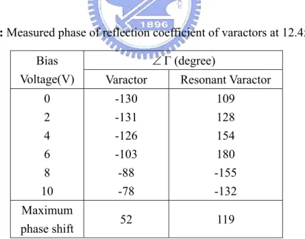
The characteristic of reflection loads with RF virtual ground and with via holes for ground are measured against bias voltage from 0V to 10V at 12.45GHz. Measured phase shift of reflection coefficient of varactor diodes is shown in Table 2.1. As predicted, the varactor with a RF virtual ground operates like a capacitance and has a phase shift range of 52o. However, the phase shift range of the resonant varactor is
improved to 119o. The later is 67o more than the former. The reflection coefficient of
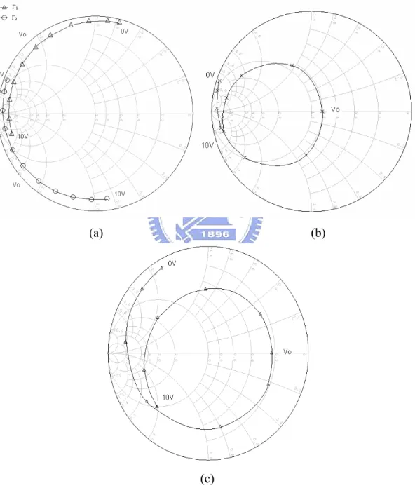
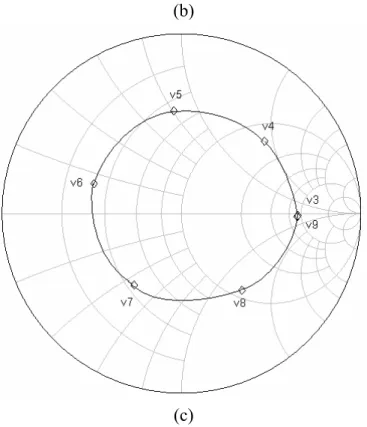
the resonant varactor is plotted for the voltage range of 0V to 10V in 1V steps on the Smith Chart in Figure 2.6, where the equivalent resistance varies with its bias voltage, as listed in Table 2.2.
Table 2.1: Measured phase of reflection coefficient of varactors at 12.45GHz
∠ Γ (degree) Bias
Voltage(V) Varactor Resonant Varactor
0 -130 109 2 -131 128 4 -126 154 6 -103 180 8 -88 -155 10 -78 -132 Maximum phase shift 52 119
Table 2.2 Measured resistance of the resonant varactor against bias voltage.
Bias voltage(V) 0 2 4 6 8 10
Figure 2.6: The reflection coefficient of the resonant varactor on the Smith Chart
2.2.3 Parallel
Resonant
Load
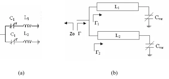
According to [2], if two branches of the varactors, each varactor being tuned with a series inductor to resonate at the low and high bias voltage (Vmin and Vmax)
respectively, are connected in parallel to form a parallel resonant circuit at a control voltage between Vmin and Vmax, the phase shift could cover 360o when the varactors
are biased form Vmin and Vmax. This can be realized if the original resonant loads at
different bias voltage are transformed by adding the transmission line with different length [9] (Figure 2.7). However, controlling the inductance of lump elements is so difficult at high frequency that transmission line is adopted in the proposed circuit.
(a) (b)
Figure 2.7: Two series resonant varactor forming a parallel resonant circuit using (a) lump elements (b) transmission lines.
By tuning the length of the transmission line, the phase of each branch can be controlled arbitrarily. The reflection coefficient of each branch is shown in Figure 2.8(a), where V0 represents the point of equal control voltage when Γ1 and Γ2 are
complex conjugate of each other. Instead of the maximum and minimum bias voltage of 0V and 10V, the series resonance is designed at bias voltage of 2V and 9V, which will be explained later. These two branches are connected in parallel to form a 360o
reflective network when the varactor is biased from 2V to 9V, as shown in Figure 2.8(b). It is apparent that the reflection coefficient of the reflection load doesn’t follow a constant ρ circle on the Smith Chart due to the series resistance RS of the varactor.
The resistance is 1.7Ω and 3.5Ω at the series resonance. However, at the parallel resonance the return loss is much higher because the equivalent parallel resistance is
2 2 0 0 0 0 0 0 0 0 ( ) //( ) 2 2 2 P 0 R X X R R jX R jX R R = + − = + ≈ (2.1)
where R0, X0 represent the equivalent resistance and reactance of one branch at bias
voltage of V0. For R0 = 2.8Ω and X0 = 19Ω, the parallel resistance RP is approximately
65Ω and the return loss is 20dB.
(a) (b)
(c)
Figure 2.8: Two series resonant varactor forming a parallel resonant circuit. (a) Two series resonant varactor. (b) Parallel resonant circuit. (c) Modified parallel circuit.
2.2.4 Changing Port Impedance of Reflection Loads
In order to increase RP and reduce the return loss at the parallel resonance, the port
impedance of the reflection load is changed. For RS and RP giving the same reflection
at series and parallel resonance, the port impedance is chosen to be
0 S P
Z = R R (2.2)
It shows that RS is 3Ω at the series resonance point or bias voltage of 9V. Thus,
from (2.2) the optimized port impedance should be 14Ω to have a minimum return-loss variation. The reason for choosing the series resonance at bias voltage of 2V and 9V is to avoid extreme RS when bias voltage is 0, 1, and 10V. The reflection
coefficient of the modified parallel circuit is shown in Figure 2.8(c).
For transforming port impedance from 50Ω to 14Ω, a quarter-wave impedance transformer is used with its characteristic impedance of 26Ω. This is too low for microstrip line to be realized. Therefore, two cascaded quarter-wave impedance transformers are used in the proposed phase shifter. The principle of impedance transforming is illustrated in Figure 2.9. The equation of the input impedance Zin
which is related to the characteristic impedance Z1, is derived as
2 2 0 0 2 2 1 1 0 ( ) in X 3 0 Z Z Z Z Z Z Z Z = = = (2.3)
Figure 2.9: Two cascaded quarter-wave impedance transformers
If the input impedance Zin is designed as 14Ω and port impedance Z0 of 3-dB
hybrid 90o coupler is 50Ω, from (2.13) the characteristic impedance Z
1 is obtained to
be 90Ω. Thus, we can use two cascaded quarter-wave impedance transformers with characteristic impedance of 90Ω and 50Ω to transform port impedance from 50Ω to 14Ω over a moderate bandwidth.
2.3 Simulation Results
The proposed 360o reflection-type phase shifter is fabricated on a substrate with a
dielectric constant of 3.58 and thickness of 20 mils. Full-wave EM simulation (Sonnet) is used to model the effects of via holes and tee-junctions of the branch line coupler and transmission lines. The circuit layout of the proposed circuit is shown in Figure 2.10 and the design parameters and physical dimensions are listed in Table 2.3, where W and L denote the width and length of the microstrip line, and D denotes the diameter of the via hole.
Figure 2.10: The circuit layout of the proposed 360o reflection-type phase shifter.
Table 2.3 Physical dimensions of the proposed 360o reflection-type phase shifter.
W1 W2 W3 W4 W5 W6 W7 W8 D
66 46 14 90 116 45 49 45 10
L1 L2 L3 L4 L5 L6 L7 L8 L9
134 138 88 152 152 118 46 217 28 (Unit: mil)
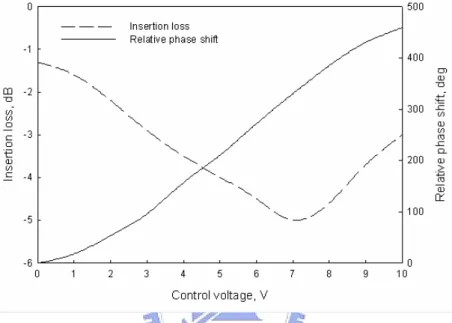
The Simulated results of relative phase shift and insertion loss against control voltage at 12.45GHz are shown in Figure 2.11. With the shunt connection of two resonant loads, the phase shift of the phase shifter is more than 360o when bias voltage is raised from 0V to 10V. It shows that the insertion loss with bias voltage
below 3V is much smaller than other biasing conditions. In order to minimize the fluctuation of the insertion loss, the phase shifter is designed to operate at the bias voltage of 2V-9V, and within the bias voltage a total phase shift of 360o can be
achieved. The scattering parameter S21 is plotted on the Smith Chart in Figure 2.12.
Figure 2.11: Simulated relative phase shift and insertion loss of proposed 360o phase
shifter at 12.45GHz.
2.4 Fabrication and Measurements
The 360o reflection-type phase shifter was fabricated on RO4003 substrate with a
20-mil thickness and a dielectric constant of 3.58 using a copper etching process. The diameter of via hole is 10 mils, and four flip-chip varactor diodes are mounted using a low temperature indium solder. The photograph of the proposed phase shifters is shown in Figure 2.13.
Figure 2.13: Photograph of the proposed 360o reflection-type phase shifter
2.4.1 Performance
against
Control
Voltage
Figure 2.14 shows measured performance with respect to varactor control voltage of the proposed 360o phase shifters at 12.45 GHz. The measured maximum phase shift is
450 o for the control voltage range of 0V-10V. It shows that for the control voltage
range of 3V to 9V, a phase shift of 360o is achieved, and the average insertion loss is
5.1 dB and its variation is ±1.3 dB. The scattering parameter S21, which is plotted in
extreme control voltages. Figure 2.15 shows the comparison of relative phase shift between the proposed 360o phase shifter, series resonant varactor, and a single
varactor.
360o
(a)
(b)
(c)
Figure 2.14: Measured results of the proposed 360o phase shifter against control
voltage at 12.45GHz. (a) Relative phase shift. (b) Insertion loss. (c) S21 on Smith
Chart.
2.4.2 Performance
against
Frequency
The measured frequency response is measured in Figure 2.16 from 12.2 to 12.7 GHz. The measurement is plotted at control voltage of 3V-9V, where a full 360o phase
shifter is achieved. It shows that the maximum phase shift is larger than 360o,
insertion loss is 4.8 1.6 dB, and return loss is better than 14 dB over 500MHz of the voltage stage of 3V-9V.
±
(b)
(c)
Figure 2.16: Frequency response of the 360o phase shifter. (a) Relative phase shift. (b)
Chapter 3
Ku band Phased array
3.1 Introduction
Phased array plays an important role in microwave applications such as radar systems and smart antenna systems of wireless mobile communication. In a phased-array antenna system, phase shifters are used to control the radiation direction. These phase shifters have to meet high requirements for continuously adjustable phase shift. Design of these phase shifters requires consideration of many factors such as large phase shift, low insertion loss, low phase error, bandwidth, low insertion-loss variation, simple control, low DC power consumption, and low cost for commercial wireless communication.
Reflection-type phase shifters (RTPS) have the advantages of simple control, low reflection, and low insertion loss. Using active components such as varactor diodes as reflection loads was first introduced in [1]. Thus, phase shift is restricted by tunable capacitance of varactor diodes. In order to maximize phase shift range of reflection loads, many approaches were reported. But when working on an effort to increase the phase shift range of phase shifters, insertion-loss variation increases. This
insertion-loss variation can be eliminated by adding a compensating resistance parallel to the reflection load [2]. Furthermore, in adaptive antenna receivers, the insertion loss and the insertion-loss variation can be compensated by the variable-gain low-noise amplifiers (VGLNA) located in front of the phase shifters.
In this chapter, a Ku band (12.2-12.7GHz) phased array using reflection type analog phase shifter is proposed. First, a phase shifter with large phase shift is discussed. Instead of using two varactors for each reflection load of the proposed 360o
phase shifter in the previous chapter, the phase shifter uses only one varactor as the reflection load. We extends the maximum phase shift of the varactor, which was originally limited by the capacitance tuning range, from 52o to 286o by resonating the
varactor with via inductance and using impedance transformers between the branch line coupler and the varactor. The circuit analysis, design procedure, and tradeoffs between phase shift range and insertion-loss variation are elaborately discussed. Finally, a 4-element phased array with a group of dipole antennas and the proposed phase shifters is fabricated to verify the proposed phase shifter. Low noise amplifiers (LNA) are used to compensate the insertion loss of phase shifters.
3.2
Theory of Reflection-Type Phase Shifter
hybrid coupler and two identical reflection loads has been discussed in chapter two. In this chapter, however, the phase shifter uses only one varactor for each reflection load. The analysis, design procedure, and fabrication of the phase shifter will be discussed.
3.2.1 Analysis
In the simplest design, a single varactor used as reflection loads is shown in Figure 3.1(a). The phase of reflection coefficient is determined by the maximum capacitance variation of the varactor diode. The phase shift can be increased by adding an inductance LS in series to the varactor, forming the series resonant circuit
(Figure 3.1(b)). The maximum phase shift range is achieved at the resonance frequency 0 0 1 S L C ω = (3.1)
where C0 represents the average capacitance value of the varactor.
To simplify this model, the parasitic resistance of the varactor and series inductance is combined as RS. Also, the inductance LS includes the parasitic inductance of the
varactor. In the ideal case (RS = 0), the phase shift of reflection coefficient follows the
unity circle of the Smith Chart. But for real varactor diodes with finite Q, the effective series resistance RS must be included in the circuit model. In this case, the reflection
resistance determines the insertion loss and insertion-loss variation with the varactor bias voltage.
(a) (b) (c)
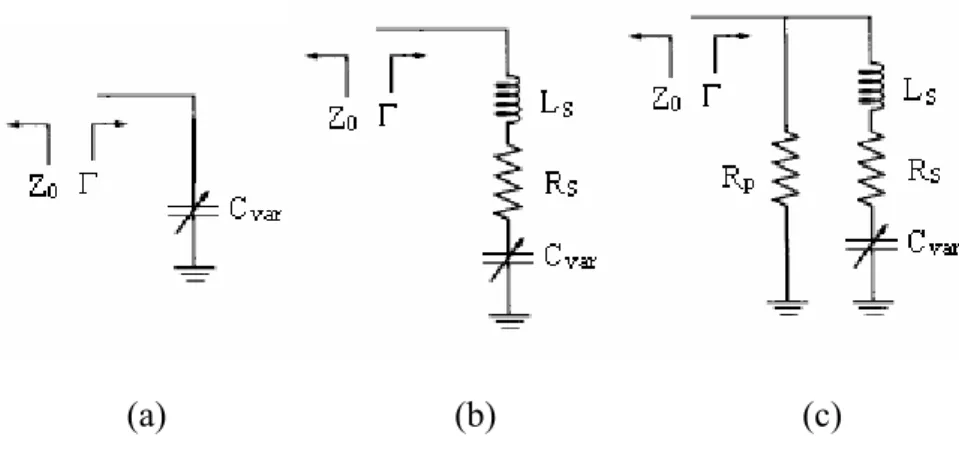
Figure 3.1: Circuit model of reflection loads, (a) Varactor. (b) Series resonant varactor. (c) Series resonant loads with compensating resistance.
A method for compensating the insertion-loss variation is to shunt a resistance RP to
the series resonant load as shown in Figure 3.1(c). This compensating resistance is used to transform the constant resistance circle locus to a constant ρ circle on the Smith Chart. Then, the insertion loss maintains nearly constant and insensitive with the change of varactor bias voltage.
3.2.2 Design
Formula
The reflection coefficient Γ of the reflection load in Figure 3.1(c) is given by
0 0 0 0 ( ) ( ( ) ( p s p s L p j p s p s L p 0 0 ) ) R R R Z R Z jX R Z e R R R Z R Z jX R Z φ + − + − Γ = Γ = + + + + (3.2)
where XL is equal toωLS −1ωCvar. Thus, phase shift and return loss of the reflection load are 0 0 1 1 0 0 0 ( ) ( ) tan L p tan L p p s p s p s p s X R Z X R Z 0 R R R Z R Z R R R Z R Z φ = − − − − + + − + + (3.3) 2 2 2 0 0 0 2 2 0 0 0 ( ) ( RL ( ) ( p s p s L p p s p s L p 2 2 ) ) R R R Z R Z X R Z R R R Z R Z X R Z + − + − = Γ = + + + + (3.4)
Since reflected signals are combined from two identical reflection loads at the output of the 3-dB 90o hybrid coupler, the scattering parameter S
21 of the phase shifter
is obtained as jα2 Γ, whereαis the loss of the 3-dB 90o hybrid coupler. Phase shift ∠S21 and insertion loss |S21| of the phase shifter is
0 0 1 1 21 0 0 0 0 ( ) ( ) tan tan 2 2 L p L p p s p s p s p s X R Z X R Z S R R R Z R Z R R R Z R Z π π φ − − − + ∠ = + = − + + − + + (3.5) 2 2 2 0 0 0 2 2 2 2 0 0 0 ( ) ( IL ( ) ( p s p s L p p s p s L p 2 2 ) ) R R R Z R Z X R Z R R R Z R Z X R Z α α + − + − = Γ = + + + + (3.6)
From (3.5) and (3.6), the varactor reactance determines not only the relative phase shift but also the insertion loss. The maximum phase shift Δφ is
,max ,min 21 XL 21 S S φ Δ = ∠ − ∠ L X (3.7)
For a given varactor capacitance range, the maximum phase shift can be increased by lowering the impedance level Z0 at the input of the reflection load, while the input
and output impedance level of the 3-dB 90o hybrid coupler is unchanged.
capacitance is. Detailed equations have been derived in [9] to achieve maximum phase shift while remaining insertion loss constant. The optimal compensating resistance is derived as 2 2 0 0 2 1 1 2 s comp s Z R R R Z ⎡ ⎛ ⎞ ⎤ ⎢ ⎥ = + + ⎜ ⎟ ⎢ ⎝ ⎠ ⎥ ⎣ ⎦ (3.8)
While the maximum relative phase shift with constant insertion loss is
2 2 0 0 0 1 max 2 2 2 0 0 0 0 ( 4 2 ) 4 tan 2 ( )( 4 ) 2 S S L S S Z Z Z R R X Z S Z R Z Z R R φ − ⎡⎢Δ + + + ⎤⎥ Δ = ⎢ + + + + ⎥ ⎣ ⎦ (3.9)
3.3 Design Procedure of Ku Band Reflection-Type
Phase Shifter
The design procedure of the proposed Ku band reflection-type phase shifter is as the following steps:
Step 1) Measure the characteristics of the varactor. Then, resonate the varactor by adding a series inductance LS.
Step 2) Change port impedance of the reflection load depending on the required maximum phase shift. Phase shift may be increased by lowering the impedance level Z0. Optimum design uses highest Z0 to produce necessary
phase shift range
3.3.1 Series
Resonant
Varactor
The varactor diode MA-COM MA46H120 is used as the termination load of the proposed 360o reflection-type phase shifter. In the previous chapter, we have shown to extend the phase shift from 52 o to 119o with the resonant load by adding via inductance to the varactor.
3.3.2 Changing Port Impedance of Reflection Loads
For a given varactor capacitance range, the maximum phase shift can be increased by lowering the impedance level Z0 at the input of the reflection load. Since the resonant
inductance LS of the proposed phase shifter is made of via holes, the value of LS is
somewhat different to the optimal resonant inductance. In order to achieve maximum phase shift, a short transmission line L1 with phase delay of 6o is added in front of the
varactor load as shown in Figure 3.2(a). The transmission line changes the phase of reflection coefficient of the reflection load, making the maximum and minimum phase of reflection coefficient vertically symmetry on the Smith Chart, as shown in Figure 3.2(b).
(a) (b) Figure 3.2: (a) Varactor load with a transmission line with L1=6o. (b) Reflection
coefficient on the Smith Chart.
To simplify the effect of the port impedance on the maximum relative phase shift, the cases of reflection loads without compensating resistance RP is considered. Figure
3.3 shows examples of reflection coefficient with different Z0 of 25Ω and 12.5Ω on
the Smith Chart. It is shown that lowering the port impedance Z0 increases not only
the maximum phase shift but also insertion-loss variation, which is the tradeoff of phase shifter design. Figure 3.4 shows design charts of maximum phase shift values and insertion-loss variations of phase shifter with respect to port impedance Z0.
(a) (b) Figure 3.3: Reflection coefficient of reflection loads at 12.45 GHz.
(a) Z0=25Ω, maximum phase shift = 195o. Insertion loss variation = 1.4dB.
(b) Z0=13Ω, maximum phase shift = 266o. Insertion loss variation = 2.8.dB.
(b)
Figure 3.4: (a) Maximum phase shift and (b) Insertion loss variation against port impedance Z0
In [9], an impedance-transforming branch line coupler is applied to the phase shifter. However, if the required impedance Z0 is very low, the impedance
transforming branch line coupler is too hard to be realized. In the proposed phase shifter, Z0 was designed at 9Ω, which is impossible for microstrip line fabrication. So,
two cascaded quarter wave impedance transformers are implemented between a conventional 3-dB 90o hybrid coupler and the reflection load to produce an adequately
low impedance level.
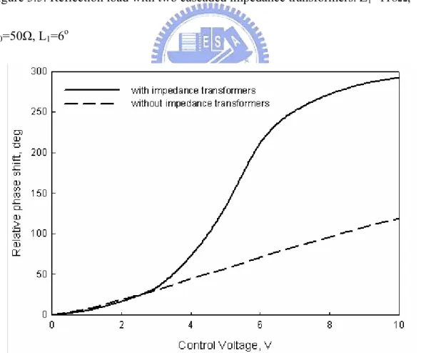
relative phase shift with and without impedance transformers is depicted in Figure 3.6. With the help of two cascaded impedance transformers, maximum phase shift of 292o,
which is 173o more than the other one, is given with the same bias voltage condition.
Figure 3.5: Reflection load with two cascaded impedance transformers. Z1=118Ω,
Z0=50Ω, L1=6o
Figure 3.6: Comparison of phase shift of the reflection load with and without impedance transformers.
3.3.3 Compensation for Insertion-Loss Variation
Given in Figure 3.4, the insertion-loss variation is 4.3 dB for the phase shifter when maximum phase shift of 292o is chosen. With the help of a compensation resistance
RP parallel to reflection loads shown in Figure 3.7, insertion-loss variation can be
eliminated. The optimized compensating resistance RP is chosen to be 200Ω. The
principle of compensation for insertion-loss variation is illustrated in Figure 3.8. Equivalent conductance at high/low control voltage is dominated by the compensating resistance. With optimized RP, the reflection coefficient of the reflection load follows
almost constant ρ circle on the Smith Chart. However, constant insertion loss is unavailable because RS varies with the bias voltage. But (3.8) is still useful for initial
design.
Figure 3.7: Reflection load with compensating resistance RP. Z1=118Ω, Z0=50Ω,
Figure 3.8: Reflection coefficient of the reflection load on the Smith Chart.
Figure 3.9 shows simulated reflection coefficient of reflection loads with and without RP. With RP =200Ω, insertion-loss variation is 1 dB and maximum phase shift
is 287o. The use of R
P barely influences maximum phase shift range.
(b)
Figure 3.9: Comparison of simulated reflection loads with and without RP at 12.45
GHz. (a) Relative phase shift and (b) Return loss of the reflection load against bias voltage of varactor.
3.4 Fabrication and Measurements of Ku Band
Reflection-Type Phase Shifter
The proposed reflection-type phase shifter was fabricated on RO4003 substrate with a dielectric constant of 3.58 and thickness of 20 mils to verify the phase shifter design procedure. The phase shifters were designed with and without the compensating resistance RP, which has been described in detail at the pervious section. Then, a 3-dB
220Ω chip resistor with fan stub as ground was used as the compensating resistance
RP. The photograph of the proposed phase shifters is shown in Figure 3.10.
(a) (b)
Figure 3.10: Photograph of the proposed phase shifter circuits (a) without RP (b) with
RP=220Ω
3.4.1 Performance against Control Voltage
Figure 3.11 shows measured performance with respect to varactor control voltage of the proposed two phase shifters without RP and with RP =220Ω. The measured
maximum phase shift of phase shifter is 286 o without R
P and 283 o with RP =220Ω. In
Figure 3.9(a), the simulated maximum relative phase shift, which is 292 o without R
P
and 287 o with R
The measured insertion-loss variation of phase shifter is 4 dB without RP and 3.5
dB with RP=220Ω. In Figure 3.9(b), the simulated insertion loss variation is 4.5 dB
without RP and 1 dB with RP=200Ω. The measured insertion loss of phase shifter
without RP agrees with the simulated results. But in the case of RP=220Ω, the
compensating resistance slightly influences the insertion-loss variation. This is mainly because the unwanted package capacitance of the chip resistor is parallel to the reflection load at high frequency of 12.45 GHz. The parallel capacitance and other parasitic effect can be observed from the S21 of the phase shifter on the Smith Chart
shown in Figure 3.12.
(b)
Figure 3.11: Measured results of the proposed phase shifters against bias voltage at 12.45 GHz. (a) Relative phase shift. (b) Insertion loss
3.4.2 Performance
against
Frequency
Because the frequency response is mainly determined by the 3-dB 90o hybrid coupler
and the cascaded quarter-wave impedance transformers, only the case of the one without RP is concerned. Figure 3.13 shows the measured performances such as phase
shifts, insertion loss, and return loss of the phase shifters without RP over the
bandwidth of 12.2 GHz to 12.7 GHz. The Figure shows that insertion-loss variation is within +2dB, return loss is better than -12dB, and phase shift is more than 280o over
500MHz at the phase stages of bias voltage from 0V to 10V.
(b)
Figure 3.13: Measured frequency performance of the proposed phase shift. (a) Insertion loss. (b) Return loss. (c) Relative phase shift.
3.5 Ku Band Phased Array
3.5.1 Theory
A phased array is a group of antennas in which the relative phases of the signals feeding the antennas are varied, so the radiation pattern of the array is reinforced in the desired direction and suppressed in undesired direction. The proposed phased shifters are used in the phased array as beamformers to provide high-speed beam-steering and high directivity. As shown in Figure 3.14, the phased array is a combination of N antennas with equidistance, and the array factor (AF) is defined as
N ( sin ) 0 jn d n n
AF
A e
β θ α+ ==
∑
(3.10)where An represents the amplitude of the signal radiated by the n-th element; α and d
represent the phase shift and distance between successive antennas, respectively. Letψ β= dsinθ + , then α
N 0 jn n n
AF
A e
ψ ==
∑
(3.11)We can see that the maximum energy is derived whenψ = . That is, 0
sin
d
α
= −
β
θ
(3.12) Therefore, if we want to control the angle at which the maximum power is emitted or received (main beam), we only need to adjust the phase shift α of successive antennas.Figure 3.14: Phased array composed of N antennas with equidistance.
Now space the antennas a distance d of 1.03 λ at center frequency of 12.45 GHz. Chosen N=4, the simulated radiation patterns with different phase shift α are shown in Figure 3.15. Each element of the phased array is assumed to be omnidirectional for simplicity. It shows that for d being approximately one wavelength, there are 4 or 5 main lobes. Considering the first quadrant (left-top), the angle of the main lobe θ is 0o,
8o, 16o, 30o, 46o, and 59o, when phase shift α is 0o, -50o, -100o, -180o, -260o, and -310o,
respectively. Figure 3.16 shows the relationship between α and θ at the first quadrant. It shows that the direction of main beam can be arbitrarily controlled if a full 360o
Figure 3.15: Simulated radiation pattern of 4-element phased array.
Figure 3.16: Relationship between the angle of main beam and phase shift between successive antennas.
3.5.2 Design
The structure of the proposed phased array with 4 elements is shown in Figure 3.17. The series-feed phased array is used for simplicity of control, and dipole antennas are used for omnidirectional radiation pattern. Then, the received signals are coupled to the signal path by a directional coupler. With the same control voltage of phase shifter, each phase shift between successive antennas is identical to the others. However, the phase shifters accumulate insertion loss along the path. In order to receive the same power from each antenna at the output port, a low noise amplifier is added in front of each phase shifter to compensate the insertion loss.
Figure 3.17: The structure of the proposed phased array. (RTPS: reflection-type phase shifter. LNA: low noise amplifier)
3.5.3 Fabrication and Measurements
The photograph of the proposed Ku band phased array is shown in Figure 3.18, in which the components of the phased array are illustrated. The phased array is designed at the center frequency of 12.45 GHz, with its size of 10×4 cm2. Dipole
antennas are chosen for omnidirectional. The directional coupler is designed with a coupling factor of -14 dB and its through port is terminated with a 50Ω resistor. The received signal is coupled to its coupled port and direct to the output port of the phased array.
Figure 3.18: Photograph of the proposed phased array. (a) Dipole antenna. (b) Directional coupler. (c) Reflection-type phase shifter. (d) Low noise amplifier. (e) Chip resistor (100Ω). (f) Control voltage of phase shifters (0-10V). (g) LNA bias voltage (1.5V).
Figure 3.19 shows the radiation pattern of the proposed phased array against different control voltage of the phase shifter. It was measured at 12.2, 12.45, and 12.7 GHz, which is the band of broadcasting satellite service (BSS). Even if the insertion loss is compensated by LNA, the radiation gain suffers from the insertion-loss
variation with control voltage of the phase shifter. The angle of main beam against control voltage is shown in Figure 3.20.
(a)
(c)
Figure 3.19: Measured radiation pattern of the proposed Ku band phased array at (a) 12.2 GHz. (b) 12.45 GHz. (c) 12.7 GHz
Chapter 4
Reduced-Size Impedance-Transforming
Broadband 180
o
Hybrid Ring
4.1 Introduction
The 180o hybrid ring coupler, which is also known as a rat-race ring, is an essential
component in microwave circuits, such as balanced mixers, multipliers, push-pull amplifiers and antenna feed network, etc. A conventional a rat-race ring consists of three λ/4 line sections and one 3λ/4 line section. The 3λ/ 4 line section works as a λ/4 line section with a phase inverter formed by a λ/2 line section. Thus, the disadvantage of the conventional rat-race ring is narrow bandwidth and large size.
Many researches [10]-[14] have attributed to make the bandwidth larger. Most of the approaches are realizing an ideal or broadband phase inverter. Replaced the 3λ/ 4 line section with a short-circuited λ/ 4 coupled line section of March [10], which not only reduce size but also widen the bandwidth of the rat-race ring. However, the tight coupled line is hard to be realized. An ideal phase inverter, which is shown in Figure 4.1(a), provides perfect amplitude and phase performance. In [11], [12], the combination of coplanar waveguide (CPW) and coplanar strips (CPS) or slot lines
was used in the 180 o hybrid ring. In these designs, frequency independent phase
inverter of the hybrid ring has been implemented by CPS direct cross-type phase inverter. Another technique to increase the bandwidth is by converting baluns into 180o hybrid ring by adding an in-phase power splitter presented in [13]. In addition to
realizing the broadband phase inverter, increasing the order of circuit response may widen the bandwidth as well. In [14], a broadband Chebyshev-response rat-race ring with a λ/4 unit element at each port and an ideal phase inverter is proposed.
Many approaches [15]-[19] have been presented to reduce the size of hybrid rings. These methods include the use of folded lines [15], artificial lines [16], defected ground structure [17], lump elements [18], and others [19]. However, the above approaches are hard to achieve a wide bandwidth. In [20], both wideband and size reduction are achieved by an interdigital CPS inverter.
In this chapter, a reduced-size impedance-transforming broadband 180 o hybrid ring
coupler is presented. With a unit element at each port and an ideal phase inverter, which was proposed in [14], the broadband rat-race ring with a Chebyshev response of order 3 or 4 has been developed. In [21], the author modified the coupler and developed the design and optimization method of a 180 o hybrid ring for Chebyshev
equiripple functions including impedance transformation between the input and output ports, as shown in Figure 4.1(b). The values of the admittance Y1, Y2, Yt1, and
Yt2 in Figure 4.1(b) are determined by the optimization method to synthesize a
broadband rat-race ring with an impedance transforming ratio of 1:3. We replace each line section by the stepped-impedance CPS/interdigital CPS structure proposed in [20] not only to realize an ideal 180 o phase inverter but also miniaturize the circuit size. A
miniaturized broadband 180o hybrid ring coupler with impedance transformation of
from 40Ω to 120Ω using the stepped-impedance CPS/interdigital CPS structure is realized. The circuit analysis, design procedure, simulation and measurement results are discussed in this chapter.
(a)
(b)
Conventional 180o hybrid ring. (b) Proposed broadband 180o hybrid ring with
different impedance at input and output ports.
4.2 Theory
4.2.1 Conventional 180
oHybrid Ring
The circuit schematic of an 180o hybrid ring with an ideal phase inverter is shown in
Figure 4.1(a). Instead of a conventional rat-race ring composed of three λg/4 and one
3λg/4 line sections, the spacing between all adjacent ports is λg/4, and an ideal phase
inverter is placed between two of the adjacent ports. With the use of an ideal phase shifter, the bandwidth of 180o hybrid ring is further increased. Even- and odd-mode
equivalent circuits of the hybrid ring are shown in Figure 4.2(a) and (b).
(a) (b)
Figure 4.2: (b) Even- and (b) Odd-mode equivalent circuits of the 180o hybrid ring
with an ideal phase inverter.
1
2 1 2
1 0 cos 2 sin 2 1
tan 1 sin 2 cos 2 cot 1
e e e e A B jZ C D jY jY jY θ θ θ θ θ ⎡ ⎤ ⎡ ⎤ ⎡ ⎤ ⎡ = ⎢ ⎥ ⎢ ⎥ ⎢ ⎥ ⎢− ⎣ ⎦ ⎣ ⎦ ⎣ ⎣ ⎦ 0 θ ⎤ ⎥ ⎦ 0 θ ⎤ ⎥ ⎦ (4.1) 1 2 1 2 1 0 cos 2 sin 2 1
cot 1 sin 2 cos 2 tan 1
o o o o A B jZ C D jY jY jY θ θ θ θ θ ⎡ ⎤ ⎡ ⎤ ⎡ ⎤ ⎡ = ⎢ ⎥ ⎢− ⎥ ⎢ ⎥ ⎢ ⎣ ⎦ ⎣ ⎦ ⎣ ⎣ ⎦ (4.2)
where Y1 and Y2 are normalized admittance of the hybrid ring, which are normalized
to port impedance Z0. Let θ=45o at the center frequency, then
2 1 1 1 2 2 2 1 2 1 2 2 45 1 1 1 1 0 0 1 0 1 0 1 o e e e e Y j Y Y A B jZ A B C D jY jY jY Y Y Y C D j Y Y θ = ⎡ ⎤ ⎢ ⎥ ⎡ ⎤ =⎡ ⎤ ⎡ ⎤ ⎡ ⎤=⎢ ⎥ ⎡ ⎢ ⎥ ⎢ ⎥ ⎢ ⎥ ⎢− ⎥ ⎢ + ⎥ ⎢ ⎣ ⎦ ⎣ ⎦ ⎣ ⎦ ⎣ ⎦ ⎣ ⎦ − ⎢ ⎥ ⎣ ⎦ ⎤ = ⎥ (4.3) 2 1 1 1 2 2 2 1 2 1 2 2 45 1 1 1 1 0 0 1 0 1 0 1 o o o o o Y j Y Y A B jZ D B C D jY jY jY Y Y Y C A j Y Y θ = ⎡ − ⎤ ⎢ ⎥ ⎡ ⎤ =⎡ ⎤ ⎡ ⎤ ⎡ ⎤=⎢ ⎥ ⎡ ⎢ ⎥ ⎢− ⎥ ⎢ ⎥ ⎢ ⎥ ⎢ + ⎥ ⎢ ⎣ ⎦ ⎣ ⎦ ⎣ ⎦ ⎣ ⎦ ⎣ ⎦ ⎢ ⎥ ⎣ ⎦ ⎤ = ⎥ (4.4)
The S parameters of the four-port network are
11 22 B C S S A B C D − = = = Γ + + + (4.5a) 21 12 2 S S A B C D = = = Τ + + + (4.5b) S31 =S13 =0 (4.5c) 1 2 41 2( / )Y Y A D S A B C D A B C D − = = + + + + + + (4.5d) 1 2 32 2( / )Y Y D A S A B C D A B C D − − = = + + + + + + (4.5e)
The output power division ratio is
2 2 2 41 32 1 2 2 2 21 12 S S Y R Y S S ⎛ ⎞ = = = ⎜ ⎟ ⎝ ⎠ (4.6)
By (4.5) and (4.6), the normalized admittance Y1 and Y2 are related to return loss
many applications. For example, if an 180o hybrid ring is designed for equal power
division, that is, Y1 = Y2, it is equivalent to an in-phase power divider and a balun.
When an input signal is incident at port 1 (delta port), the balun provides 180o
out-of-phase equal power division between port 2 and 4, and no power reaches port 3. On the other hand, when power is incident at port 3 (sum port), the power divider provides in-phase power division between port 2 and 4, and no power reaches port 1.
4.2.2
Impedance-Transforming Broadband 180
oHybrid
Ring
The circuit schematic of the proposed broadband Chebyshev response 180o hybrid
ring with impedance transforming between input and output is shown in Figure 4.1(b). Instead of the conventional 180o hybrid ring with an ideal phase inverter mentioned in
the previous section, the proposed 180o hybrid ring comprises a reconfigured hybrid
ring [22] and an additional λ/4 unit element at each input and output (I/O) port. With the reconfigured hybrid ring shown in Figure 4.3(a), the input/output ports are on the same side so that it is easier to analysis the proposed circuit, which is a cascade of a single ring and unit elements. Based on even-odd mode analysis and the scattering matrix of interconnected networks, the circuit analysis of the proposed 180o hybrid
reconfigured 180o hybrid ring with an ideal phase inverter and the second part is one
pair of unit elements with the same characteristic impedance at the same side. The whole circuit is a cascading of a single-section hybrid ring and two pairs of unit elements. After the circuit analysis of each 4-port network, we can derive the scattering matrix of the overall network.
(a) (b)
Figure 4.3: Circuit schematics of (a) the reconfigured hybrid ring with an ideal phase inverter (b) one pair of unit elements with the same impedance at the same side.
Consider the single-section hybrid ring in Figure 4.3(a). Using the even-odd mode analysis, the ABCD matrices are given by
( )
⎥ ⎦ ⎤ ⎢ ⎣ ⎡ = ⎥ ⎥ ⎦ ⎤ ⎢ ⎢ ⎣ ⎡ − = ⎥ ⎦ ⎤ ⎢ ⎣ ⎡ D C B A t D t C t t tB t A t D C B A e e e e ) ( ) ( 1 ) ( ) ( 1 1 2 1 2 2 2 0 2 1 2 (4.7) ⎥ ⎦ ⎤ ⎢ ⎣ ⎡ = ⎥ ⎦ ⎤ ⎢ ⎣ ⎡ A C B D D C B A o o o o (4.8)where t = jtanθ and A, B, C, D are the polynomials of t2, where the subscripts