The investigation of charge loss mechanism in a two-bit wrapped-gate nitride
storage nonvolatile memory
Y. H. Ho, Steve S. Chung, and H. H. Chen
Citation: Applied Physics Letters 97, 183508 (2010); doi: 10.1063/1.3508956
View online: http://dx.doi.org/10.1063/1.3508956
View Table of Contents: http://scitation.aip.org/content/aip/journal/apl/97/18?ver=pdfcov Published by the AIP Publishing
Articles you may be interested in
Two-bit multi-level phase change random access memory with a triple phase change material stack structure J. Appl. Phys. 112, 104504 (2012); 10.1063/1.4765742
Nonvolatile memory with graphene oxide as a charge storage node in nanowire field-effect transistors Appl. Phys. Lett. 100, 093106 (2012); 10.1063/1.3690670
Two-bit effect of trigate nanowires polycrystalline silicon thin-film-transistor nonvolatile memory with oxide/nitride/oxide gate dielectrics
Appl. Phys. Lett. 92, 163506 (2008); 10.1063/1.2910460
Vertically standing carbon nanotubes as charge storage nodes for an ultimately scaled nonvolatile memory application
Appl. Phys. Lett. 91, 063110 (2007); 10.1063/1.2767211
Memory characteristics of silicon nitride with silicon nanocrystals as a charge trapping layer of nonvolatile memory devices
Appl. Phys. Lett. 86, 251901 (2005); 10.1063/1.1951060
This article is copyrighted as indicated in the article. Reuse of AIP content is subject to the terms at: http://scitation.aip.org/termsconditions. Downloaded to IP: 140.113.38.11 On: Wed, 30 Apr 2014 09:55:42
The investigation of charge loss mechanism in a two-bit wrapped-gate
nitride storage nonvolatile memory
Y. H. Ho,1Steve S. Chung,1,a兲and H. H. Chen2
1Department of Electronics Engineering, National Chiao Tung University, Hsinchu 300, Taiwan 2United Microelectronics Corporation (UMC), No. 3, Li-Hsin 2nd Road, Hsinchu 300, Taiwan
共Received 6 August 2010; accepted 9 October 2010; published online 5 November 2010兲
The charge loss mechanism of a two-bit wrapped-gate nitride storage nonvolatile memory is investigated. From retention measurements, it was shown that both vertical and lateral charge loss coexist. As a result of the misalignment of carriers, the lateral charge loss was caused by the hole accumulation near the junction and migrating toward the channel. By using a scaling of the word-gate length or a substrate-transient hot hole erase scheme, the charge loss in the lateral direction can be suppressed. Also, from the retention test, the latter scheme, substrate-transient hot hole 共STHH兲, has a window independent of the word-gate length, which is better for the device scaling.
© 2010 American Institute of Physics.关doi:10.1063/1.3508956兴
Silicon-oxide-nitride-oxide-silicon 共SONOS兲 flash memory is one of the most mature nitride-storage technolo-gies, which allows one-bit/cell or two-bit/cell operation by using channel-hot-electron 共CHE兲 injection programming and band-to-band hot-hole 共BBHH兲 injection erasing.1,2 However, the conventional SONOS flash memory has some disadvantages such as low programming efficiency, high power consumption, and high programming drain voltage, etc.
Another important issue related to the SONOS cell is the charge loss with time, the data retention. Two major models have been reported to explain the retention mechanisms. The first model is the vertical charge loss through bottom oxide, since the bottom oxide is strongly degraded during succes-sive P/E stresses.3–6The trapped electrons in the nitride stor-age can escape through Frankel–Pool tunneling and trap-assist-tunneling to the substrate. The second model explains the charge loss through the lateral redistribution of holes be-cause of a misalignment.6–9 After long term P/E cycles, a large amount of holes accumulation near the junction, the holes might spread out and migrate into the channel before recombining with the programmed electron through thermal activation. In recent years, a SONOS-type memory cell with wrapped gate was demonstrated,10,11 which is feasible for high density, high speed, and low power consumption. By utilizing source-side-injection 共SSI兲 programming, the wrapped-gate SONOS can achieve hundred times better ef-ficiency than CHE ones.10,11However, none has been studied on the reliability issues of such device, especially the data retention. With the specific structure of wrapped-gate SONOS, we can take the advantage to suppress the misalign-ment of charge distribution. The mechanism of this approach will be proposed.
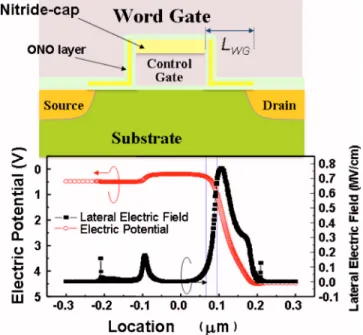
Figure 1 shows the device structure and the simulation result by using SYNOPSYS SENTAURUS TCAD 共technology
computer aided design兲 software.12
The device has a control gate wrapped by the ONO layer and then a word gate is grown on the top. A nitride-cap layer共300 Å兲 was grown on top of the control gate and with a tunnel oxide共65 Å兲 at the
bottom. From the TEM cross-section, the experimental de-vices have ONO layer thickness, with 65 Å bottom oxide, 60 Å nitride, and 80 Å top oxide. The ONO-layer was cutoff by the self-alignment process at the edge of the source/drain, and the oxide thickness between word gate and the source/ drain region is about 500 Å. The gate width is about 0.2 m, and the channel length is 0.18 m under the control-gate and with three different splits of 0.10, 0.12, and 0.13 m for the word-gate length, LWG. It was shown that the gap region has the largest electric potential drop and forms a largest lateral electric field. Therefore, the electron will get sufficient energy in the gap region, inducing impact ionization to achieve programming operation. The programming charge should be injected to the right 共left兲 side of the word-gate between the gap and the drain 共source兲. The programming and erasing condition are shown in Table I.
a兲Electronic mail: [email protected].
FIG. 1.共Color online兲 The device structure and the simulation results of the electric potential and lateral electric field under the programming conditions, VG= 10 V, VCG= 1 V, VD= 4 V, and VB= 0 V.
APPLIED PHYSICS LETTERS 97, 183508共2010兲
0003-6951/2010/97共18兲/183508/3/$30.00 97, 183508-1 © 2010 American Institute of Physics
This article is copyrighted as indicated in the article. Reuse of AIP content is subject to the terms at: http://scitation.aip.org/termsconditions. Downloaded to IP: 140.113.38.11 On: Wed, 30 Apr 2014 09:55:42
Figure2共a兲shows the endurance by using SSI program-ming and band-to-band hot hole 共BBHH兲 injection erasing operations. The erased state threshold voltage rolls up with the increasing number of P/E cycles. For a shorter word-gate length, the programmed electrons will be more close to the junction and holes being injected from the channel which will be more easily to recombine with these electrons. In comparison, for long word-gate length, the misalignment be-comes worse since holes will be accumulated near the junc-tion, repulsing the next hole injection and creating the elec-tron accumulation in the channel so as to raise the erase state threshold voltage as shown in Fig.2共a兲. The retention experi-ment, charge loss at 85 ° C baking, is shown in Fig. 2共b兲. Since the program and erase operations are all the same for the three devices, we can assume that the bottom oxide of the three devices are equally damaged, that is, the vertical charge loss are almost the same for all three devices. Hence, the charge loss difference comes from the lateral direction. It was found that both the vertical and lateral charge loss co-exist no matter what the word-gate length was used. At the programmed state, the accumulated holes migrate into the channel and cause a decrease in threshold voltage while at the erased state, it caused an increase in the threshold volt-age. These came from the misalignment of electrons and holes as well as the migration of holes into the channel.
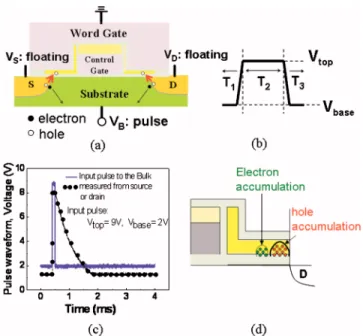
To solve the aforementioned misalignment issues, a substrate-transient hot hole 共STHH兲 injection13 erasing scheme has been proposed. Figure 3共a兲 shows the STHH erase set-up and the applying pulse is given in Fig. 3共b兲. During STHH erasing, the gate is grounded; the source and drain are kept floating while a pulse was applied to the sub-strate. From T1 to T2, source and drain are kept floating while a positive bias 共Vtop兲 is applied to the bulk, where source or drain-substrate junction capacitance is charged first 共the junction is forward biased兲. As time goes from T2to T3, the substrate bias immediately comes back to Vbasewhile the floating drain cannot catch up but slowly recovered to the initial bias condition. Therefore, a large band bending occurs
and generates hot holes to achieve erasing operation. The output 共circles兲 is measured from the drain or source, in which the voltage difference of the input pulse to the bulk and the n + source/drain is the contact potential, Vbi共around 0.5 to 0.6 V兲 between the p-n+junctions. Also, in this figure, a change in the base voltage, Vbase, the discharging transient will reach to the Vbase value. Although the applied pulse width can be very short, microsecond or less, the real erasing time is the time for floating drain moving from Vtop– Vbito Vbase– Vbi, in a few minisecond, Fig.3共c兲.
Based on the plot in Fig. 3共d兲, the holes are localized near the drain while electrons are located more close to the channel as a result of the programming and erasing schemes used. To show the efficacy of STHH injection of holes, Fig.
4 shows the endurance and the retention loss at 85 ° C bake by using SSI programming and STHH erasing operation. The threshold voltages of the erase states are almost the same even after 104 P/E cycles. It reveals that less electron and hole accumulates in the channel and near the junction. Be-cause the location of the hole profile generated by STHH is more deeply into the channel than BBHH, the holes can
TABLE I. The programming and erasing bias conditions used in this work.
Schemes VS VD 共V兲 VG 共V兲 VCG 共V兲 VB 共V兲 Time Program共SSI兲 0 4 10 1 0 4 s Erase共BBHH兲 Floating 6 ⫺5 0 0 1 ms
Erase共STHH兲 Floating Floating Floating 0 10 1 s
FIG. 2.共Color online兲 共a兲 The endurance and 共b兲 the retention loss at 85 °C baking of the wrapped-gate device after 104 P/E cycles by using SSI
pro-gramming and BBHH erasing with bias conditions listed in TableI.
FIG. 3. 共Color online兲 共a兲 The schematic set-up of the operating connections and共b兲 the input pulse waveform applying to the bulk, VB.共c兲 The
mea-sured waveform共circles兲 from the source or drain terminal, under the ap-plying pulse共solid line兲. 共d兲 The respective locations of the injected elec-trons and holes under the word-gate region and near the drain, where the ONO storage layer is underneath the word-gate.
FIG. 4.共Color online兲 共a兲 The endurance and 共b兲 the retention tests at 85 °C baking temperature of the wrapped-gate device after 104 P/E cycles by
using SSI programming and STHH erasing with bias conditions listed in TableI.
183508-2 Ho, Chung, and Chen Appl. Phys. Lett. 97, 183508共2010兲
This article is copyrighted as indicated in the article. Reuse of AIP content is subject to the terms at: http://scitation.aip.org/termsconditions. Downloaded to IP: 140.113.38.11 On: Wed, 30 Apr 2014 09:55:42
completely eliminate the programmed electrons far from the junction and lead to better alignment of electrons and holes. Figure 4共b兲 shows that the retention loss is independent of the programming gate length which can be assumed that no accumulation holes and electrons were observed. Therefore, it inhibits the charge loss through the lateral direction, and the vertical charge loss is mainly caused by the cycling-induced traps after long term P/E cycles. Furthermore, the predicted 10-year lifetime retention test shows that window closure is much better by the using of STHH scheme.
In conclusion, the charge loss in a wrapped-gate SONOS cell includes both lateral and vertical directions. The vertical charge loss is mainly determined by the generated interface traps while the lateral charge loss is caused by the misalign-ment between electron and hole accumulations during P/E cycling. For the two-bit wrapped-gate SONOS, by altering the word-gate length to a suitable length, the lateral direction loss can be moderately improved. Besides, by utilizing SSI programming and STHH erasing schemes, proposed in this paper, a complete elimination of the misalignment along the lateral direction can be achieved which results in a better window closure for the ten year life-time test.
The authors would like to acknowledge the support by
the National Science Council, Taiwan under Contract No. NSC95-2221-E009-280. The test samples were fabricated by UMC, Taiwan.
1B. Eitan, P. Pavan, I. Bloom, E. Aloni, A. Frommer, and D. Finzi,IEEE
Electron Device Lett. 21, 543共2000兲.
2L. Breuil, L. Haspeslagh, P. Blomme, D. Wellekens, J. D. Vos, M.
Loren-zini, and J. V. Houdt,IEEE Trans. Electron Devices 52, 2250共2005兲.
3W. J. Tsai, N. K. Zous, C. J. Liu, C. H. Chen, T. Wang, S. Pan, and C. Y.
Lu, Tech. Dig. - Int. Electron Devices Meet. 2001, 719.
4S.-H. Gu, T. Wang, W.-P. Lu, Y.-H. J. Ku, and C.-Y. Lu,Appl. Phys. Lett.
89, 163514共2006兲.
5R. Daniel, Y. Shacham-Diamand, and Y. Roizin, Appl. Phys. Lett. 85,
6266共2004兲.
6A. Shapira, Y. Shur, Y. S. Diamand, A. Shapira, and B. Eitan,Appl. Phys.
Lett. 92, 133514共2008兲.
7J. M. Shannon and B. A. Morgan,J. Appl. Phys. 86, 1548共1999兲. 8A. Furnemont, M. Rosmeulen, K. V. D. Zanden, J. V. Houdt, K. D. Meyer,
and H. Maes,IEEE Trans. Electron Devices 54, 1351共2007兲.
9M. Janai, B. Eitan, A. Shapira, E. Lusky, and I. Bloom, IEEE Trans.
Device Mater. Reliab. 4, 404共2004兲.
10H. Tomiye, T. Terano, K. Nomoto and T. Kobayashi, Dig. Tech. Pap.
-Symp. VLSI Technol. 2002, 206.
11H. Tomiye, T. Terano, K. Nomoto, and T. Kobayashi,Jpn. J. Appl. Phys.,
Part 1 44, 4825共2005兲.
12Sentaurus User Manual共Synopsys, Version C, 2009兲.
13S. S. Chung, Y. H. Tseng, C. S. Lai, Y. Y. Hsu, E. Ho, T. Chen, L. C. Peng,
and C. H. Chu, Tech. Dig. - Int. Electron Devices Meet. 2007, 457.
183508-3 Ho, Chung, and Chen Appl. Phys. Lett. 97, 183508共2010兲
This article is copyrighted as indicated in the article. Reuse of AIP content is subject to the terms at: http://scitation.aip.org/termsconditions. Downloaded to IP: 140.113.38.11 On: Wed, 30 Apr 2014 09:55:42