Improved crystal quality and performance of GaN-based light-emitting diodes by
decreasing the slanted angle of patterned sapphire
Ji-Hao Cheng, YewChung Sermon Wu, Wei-Chih Liao, and Bo-Wen Lin
Citation: Applied Physics Letters 96, 051109 (2010); doi: 10.1063/1.3304004
View online: http://dx.doi.org/10.1063/1.3304004
View Table of Contents: http://scitation.aip.org/content/aip/journal/apl/96/5?ver=pdfcov Published by the AIP Publishing
Articles you may be interested in
The improvement of GaN-based light-emitting diodes using nanopatterned sapphire substrate with small pattern spacing
AIP Advances 4, 027123 (2014); 10.1063/1.4867091
282-nm AlGaN-based deep ultraviolet light-emitting diodes with improved performance on nano-patterned sapphire substrates
Appl. Phys. Lett. 102, 241113 (2013); 10.1063/1.4812237
The aspect ratio effects on the performances of GaN-based light-emitting diodes with nanopatterned sapphire substrates
Appl. Phys. Lett. 97, 023111 (2010); 10.1063/1.3463471
Enhanced performance of GaN-based light emitting diode with isoelectronic Al doping layer J. Appl. Phys. 105, 064508 (2009); 10.1063/1.3095486
Enhanced light output from aligned micropit InGaN-based light emitting diodes using wet-etch sapphire patterning
Appl. Phys. Lett. 90, 131107 (2007); 10.1063/1.2714203
This article is copyrighted as indicated in the article. Reuse of AIP content is subject to the terms at: http://scitation.aip.org/termsconditions. Downloaded to IP: 140.113.38.11 On: Wed, 30 Apr 2014 11:58:38
Improved crystal quality and performance of GaN-based light-emitting
diodes by decreasing the slanted angle of patterned sapphire
Ji-Hao Cheng,1YewChung Sermon Wu,1,a兲Wei-Chih Liao,1and Bo-Wen Lin1,2
1Department of Materials Science and Engineering, National Chiao Tung University, Hsinchu 300, Taiwan 2Sino-American Silicon Products Inc., Hsinchu 300, Taiwan
共Received 21 October 2009; accepted 11 January 2010; published online 2 February 2010兲 Periodic triangle pyramidal array patterned sapphire substrates共PSSs兲 with various slanted angles were fabricated by wet etching. It was found beside normal wurtzite GaN, zinc blende GaN was found on the sidewall surfaces of PSS. The crystal quality and performance of PSS-LEDs improved with decrease in slanted angle from 57.4° to 31.6°. This is because most of the growth of GaN was initiated from c-planes. As the growth time increased, GaN epilayers on the bottom c-plane covered these pyramids by lateral growth causing the threading dislocation to bend toward the pyramids. © 2010 American Institute of Physics.关doi:10.1063/1.3304004兴
Many technique have been developed for improving the GaN-based light-emitting diodes 共LEDs兲 internal quantum efficiency 共IQE兲 and light extraction efficiency 共LEE兲, such as low temperature buffer layer,1epitaxial lateral overgrowth 共ELOG兲,2,3
surface roughening,4,5 nanoimprinting,6 metal mirror reflect layer7 and patterned sapphire substrate 共PSS兲.8–11
Currently, the PSS technique has attracted much attention for its high production yield. Using the PSS tech-nique can improve both IQE and LEE.
In this study, periodic triangle pyramidal array PSSs with various slanted angles were fabricated by wet etching. The pattern morphologic, epilayers quality, microstructure, as well as optical properties of the InGaN/GaN-LED were sys-tematically investigated.
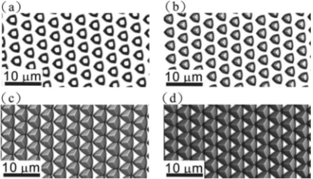
PSSs with periodic patterns 共2 m width and 2 m spacing兲 were prepared by standard photolithography. A 100 nm thick SiO2film served as the wet-etching hard mask and was deposited on the sapphire surface. As shown in Fig. 1 and TableI, four kinds of periodic triangle pyramidal arrays were etched in hot H3PO4-based solutions for various
times.12,13They were denoted as A, B, C, and D-PSS. Their confocal microscope images are shown in Fig.1. The heights of pyramids were all about 1.20 m. The struc-ture of A-PSS comprises of a triangle pyramid covered with three 兵101¯2其r-planes with a flat top c-plane. The slanted angle between the r-plane and c-plane was 57.4° as listed in Table I. The other PSSs comprise of triangle pyramids cov-ered with different兵101¯x其 共x⬎2兲 planes without top c-plane. The slanted angle between the c-plane and 兵101¯x其 planes of samples A, B, C, and D were 57.4°, 45.3°, 38.3°, and 31.6°, respectively. These slanted angles were measured using fo-cus ion beam共FIB兲 and cross section scanning electron mi-croscopy共SEM兲 images.
After the clean process, the LED structures were grown by metalorganic chemical vapor deposition. The structures comprised a buffer layer on the PSS, a undoped-GaN layer film, a n-GaN layer, a Si-doped AlGaN cladding layer, an InGaN-GaN multiple quantum well 共MQW兲 with emission
wavelength in the blue region共450 nm兲, a Mg-doped AlGaN cladding layer and a p-GaN layer.
The device mesa with a chip size of 350⫻350 m2was then defined by an inductively coupled plasma to remove Mg-doped GaN layer and MQW until the Si-doped GaN layer was exposed. After annealed at 600 ° C for 10 min, the indium tin oxide共ITO兲 layer was deposited to form a p-side contact layer and a current spreading layer. The Cr/Au layer was deposited onto the ITO layer to form the p-side and n-side electrodes.
The uniformity of device performance is addressed by the wafer mapping of dominant wavelength and forward voltage. The data are obtained at a forward current of 20 mA and with a sampling rate of 180:1, i.e.,⬃100 devices, across a 2 inch wafer. The average wavelength and forward voltage across the wafer is 448.0 nm and 3.30 V, respectively. The standard deviations of dominant wavelength and forward voltage are 2.5 nm and 0.03 V for all samples.
The average luminescence intensity and the output power of LEDs were listed in Table I. As can be seen, the performance of PSS-LEDs increased with decrease in slanted angle. When the angle decreased to 31.6°, the light intensity and the output power of D-LED were 140.0 mcd and 20.8 mW, which were 1.54 and 1.37 times higher than those of A-LED. This indicates that IQE, GaN crystal quality and LEE improved with decrease in slanted angle.
Light output measurements were conducted at various temperatures, the room temperature IQE values listed were determined by assuming 100% IQE at low temperature
a兲Author to whom correspondence should be addressed. Electronic mail:
[email protected]. Tel.: 886-3-5131555. FAX: 886-3-5724727.
FIG. 1. Confocal microscopy images of PSS: 共a兲 A-PSS, 共b兲 B-PSS, 共c兲 C-PSS, and共d兲 D-PSS.
APPLIED PHYSICS LETTERS 96, 051109共2010兲
0003-6951/2010/96共5兲/051109/3/$30.00 96, 051109-1 © 2010 American Institute of Physics
This article is copyrighted as indicated in the article. Reuse of AIP content is subject to the terms at: http://scitation.aip.org/termsconditions. Downloaded to IP: 140.113.38.11 On: Wed, 30 Apr 2014 11:58:38
共77 K兲. The measured IQEs 共int兲 of PSS-LEDs were listed
in TableI. The IQE of PSS-LEDs increased with decrease in slanted angle. When the angle decreased to 31.6°, the IQE of D-LED were 66.0%, which was 1.17 times higher than that of A-LED.
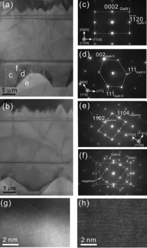
Transmission electron-microscopy 共TEM兲 and high-resolution transmission electron microscopy共HRTEM兲 were used to verify the nature of GaN crystals. Low-magnification cross-sectional TEM images of GaN grown on A-PSS and D-PSS are shown in Figs.2共a兲and2共b兲. Two kinds of GaNs were found on PSS. One共GaN I兲 was initiated from c-plane of A-PSS and D-PSS. The other共GaN II兲 was from sidewall
surfaces of A-PSS 关Figs. 2共a兲兴. Most of threading disloca-tions were initiated from c-plane. This is because most of the growth of GaN was initiated from c-planes.14,15 To realize the crystallographic relationships among GaN and sapphire substrate, selected area diffraction共SAD兲 patterns were taken from GaN I, GaN II, and PSS 关Figs.2共c兲–2共f兲兴. GaN I was wurtzite structure as shown in Fig.2共c兲. The crystallographic relationship between GaN I and sapphire is established as 共0001兲GaN I 储共0001兲sapphire and 关11¯00兴GaN I 储关112¯0兴sapphire.
This orientation relationship is usually seen in the case of a GaN epitaxially grown on a c-plane sapphire. On the other hand, it is worthy to note that GaN II was zinc blende struc-ture as shown in Fig. 2共c兲. There is no obviously crystallo-graphic relationship between GaN II and sapphire substrate. The HRTEM images of zinc blende region 共GaN II兲 and wurtzite region 共GaN I兲 are shown in Figs.2共g兲and2共h兲.
In addition to TEM, two other ways was used to evaluate the GaN crystal quality:共1兲 x-ray diffraction 共XRD兲 and 共2兲 screw dislocation density, which can be characterized by etching pit density 共EPD兲. They are summarized in TableI. XRD shows that the full-width at half-maximum 共FWHM兲 of the rocking curve decreases monotonically as the slanted angle is decreased from 57.4° to 31.6° for both the symmet-ric共002兲 and asymmetric 共102兲 reflections. This indicates the structural quality of PSS-LEDs increased with decrease in slanted angle.16 The improvement on structural quality was also verified by EPD. Samples were etched in 210 ° C H3PO4
for 2 min. As expected, the EPD was reduced from 4.31 ⫻107to 0.52⫻107 cm−2 when the slanted angle decreased
from 57.4° to 31.6°. The reduction of dislocation density also indicated that the IQE was improved.17
We believe that the observed differences in EPDs/crystal qualities were due to the change in lateral growth area of GaN. Most of the growth of GaN was initiated not from sidewall surfaces but c-planes.14,15There were following two kinds of c-planes:共1兲 top c-plane and 共2兲 bottom c-plane. As the growth time growth time increased, GaN epilayers on the bottom c-plane covered these pyramids by lateral growth, which is similar to the ELOG mode.14,15
The lateral growth area fraction共LGA兲 can be estimated by the following equation:
LGA =关1 − 共c-plane areas/total areas兲兴,
where c-plane areas include top and bottom c-plane areas. As listed in Table I, LGAs of LEDs indeed increased with de-crease in slanted angle. As a result, the EPDs on the surfaces of LEDs decreased with slanted angle. This indicates that the
TABLE I. The parameters and performances of PSS-LEDs.
Patterned sapphire substrate GaN on PSS Light-emitting diodes
Pyramid protrusion XRD FWHM 共arcsec兲 EPD 共⫻107 cm−2兲 Average intensity 共mcd兲 Output power 共mW兲 int 共%兲 Etched depth 共m兲 c-area ratio 共%兲 Slanted angle 共°兲 共002兲 共102兲 RT, 20 mA A-PSS 1.20 59.6 57.4 269.3 410.3 4.31 91.2 15.2 56.5 B-PSS 1.20 47.5 45.3 264.1 353.6 1.11 121.6 17.2 60.7 C-PSS 1.20 21.6 38.3 251.5 312.6 0.87 131.2 18.5 61.6 D-PSS 1.20 9.6 31.6 243.4. 301.2 0.52 140.0 20.8 66.1
FIG. 2. Bright-field TEM images of共a兲 A-PSS and 共b兲 D-PSS. 共c兲, 共d兲, 共e兲, and 共f兲 are SAD patterns taken from 共a兲 A-PSS. These patterns are from GaN I关共c兲兴, GaN II关共d兲兴, sapphire substrate关共e兲兴, and interface region 关共f兲兴a-mong GaN I, GaN II, and sapphire substrate.共g兲 and 共h兲 are HRTEM images of共g兲 GaN II region 共zinc blende structure兲 and 共h兲 GaN I region 共wurtzite structure兲.
051109-2 Cheng et al. Appl. Phys. Lett. 96, 051109共2010兲
This article is copyrighted as indicated in the article. Reuse of AIP content is subject to the terms at: http://scitation.aip.org/termsconditions. Downloaded to IP: 140.113.38.11 On: Wed, 30 Apr 2014 11:58:38
GaN crystal quality improved with decrease in slanted angle. The other factor might affect the light intensity and the output power is the light extraction efficiency. Monte Carlo simulation reveals that the extraction efficiency were in-creased when the slanted angle was dein-creased from 80° to 30°.18 As a result, the light extraction efficiencies of PSS-LEDs increased as the slanted angle was decreased from 57.4° to 31.6°.
In summary, periodic triangle pyramidal array PSSs with various slanted angles were fabricated by wet etching. Be-side normal wurtzite GaN, zinc blende GaN was found on the sidewall surfaces共r-planes兲 of A-PSS. The luminescence intensity, the output power, crystal quality, and light extrac-tion efficiencies of PSS-LEDs increased as the slanted angle was decreased from 57.4°共r-plane兲 to 31.6°. We believe that these observed differences were due to the change in lateral growth area of GaN, which increased with decrease in slanted angle. When the angle decreased to 31.6°, the light intensity and the output power of D-LED were 140.0 mcd and 20.8 mW, which were 1.54 and 1.37 times higher than those of A-LED.
This project was funded by Epistar Corporation, Sino American Silicon Products Incorporation, and the National Science Council of the Republic of China under Grant No. 98-2221-E009-041-MY3. Technical supports from the Na-tional Nano Device Laboratory, Center for Nano Science and Technology, Nano Facility Center and Semiconductor Laser Technology Laboratory of the National Chiao Tung Univer-sity are also acknowledged.
1H. Amano, N. Sawaki, I. Akasaki, and Y. Toyoda,Appl. Phys. Lett. 48,
353共1986兲.
2K. Linthicum, T. Gehrke, D. Thomson, E. Carlson, P. Rajagopal, T. Smith,
D. Batchelor, and R. Davis,Appl. Phys. Lett. 75, 196共1999兲.
3A. Sakai, H. Sunakawa, and A. Usui,Appl. Phys. Lett. 71, 2259共1997兲. 4W. C. Peng and Y. C. Sermon Wu,Appl. Phys. Lett. 88, 181117共2006兲. 5C. E. Lee, Y. J. Lee, H. C. Kuo, M. R. Tsai, B. S. Cheng, T. C. Lu, S. C.
Wang, and C. T. Kuo,IEEE Photon. Technol. Lett. 19, 1200共2007兲.
6H. W. Huang, C. H. Lin, C. C. Yu, B. D. Lee, C. H. Chiu, C. F. Lai, H. C.
Kuo, K. M. Leung, T. C. Lu, and S. C. Wang,Nanotechnology 19, 185301 共2008兲.
7Y. C. Sermon Wu, C. Liao, and W. C. Peng,Electrochem. Solid-State Lett.
10, J126共2007兲.
8D. S. Wuu, W. K. Wang, K. S. Wen, S. C. Huang, S. H. Lin, R. H. Hrong,
Y. S. Yu, and M. H. Pan,J. Electrochem. Soc. 153, G765共2006兲.
9J. H. Lee, J. T. Oh, Y. C. Kim, and J. H. Lee,IEEE Photon. Technol. Lett.
20, 1563共2008兲.
10C. H. Chiu, H. H. Yen, C. L. Chao, Z. Y. Li, Yu. Peichen, H. C. Kuo, T. C.
Lu, S. C. Wang, K. M. Lau, and S. J. Cheng,Appl. Phys. Lett.93, 081108 共2008兲.
11H. C. Lin, R. S. Lin, J. I. Chyi, and C. M. Lee,IEEE Photon. Technol.
Lett. 20, 1621共2008兲.
12F. Dwikusuma, D. Saulys, and T. F. Kuech,J. Electrochem. Soc. 149,
G603共2002兲.
13H. Gao, F. Yan, Y. Zhang, J. Li, Y. Zeng, and G. Wang,J. Appl. Phys. 103,
014314共2008兲.
14C.-C. Pan, C.-H. Hsieh, C.-W. Lin, and J.-I. Chyi, J. Appl. Phys. 102,
084503共2007兲.
15J. H. Lee, J. T. Oh, J. S. Park, J. W. Kim, Y. C. Kim, J. W. Lee, and H. K.
Cho,Phys. Status Solidi C 3, 2169共2006兲.
16B. Heying, X. H. Wu, S. Keller, Y. Li, D. Kapolnek, B. P. Keller, S. P.
DenBaars, and J. S. Speck,Appl. Phys. Lett. 68, 643共1996兲.
17Q. Dai, M. F. Schubert, M. H. Kim, J. K. Kim, E. F. Schubert, D. D.
Koleske, M. H. Crawford, S. R. Lee, A. J. Fischer, G. Thaler, and M. A. Banas,Appl. Phys. Lett. 94, 111109共2009兲.
18T. X. Lee, K. F. Gao, W. T. Chien, and C. C. Sun,Opt. Express15, 6670
共2007兲.
051109-3 Cheng et al. Appl. Phys. Lett. 96, 051109共2010兲
This article is copyrighted as indicated in the article. Reuse of AIP content is subject to the terms at: http://scitation.aip.org/termsconditions. Downloaded to IP: 140.113.38.11 On: Wed, 30 Apr 2014 11:58:38