IEEE ELECTRON DEVICE LETTERS, VOL. 27, NO. 9, SEPTEMBER 2006 743
Enhancement of Brightness Uniformity by a
New Voltage-Modulated Pixel Design for
AMOLED Displays
Hau-Yan Lu, Po-Tsun Liu, Member, IEEE, Ting-Chang Chang, and Sien Chi
Abstract—This letter presents a new pixel design and driving
method for active-matrix organic light-emitting diode (AMOLED) displays using low-temperature polycrystalline silicon thin-film transistors (TFTs). The proposed pixel circuit consists of five TFTs and one capacitor to eliminate the variation in the threshold voltage of the TFTs, and the drop in the supply voltage in a single frame operation by the source-follower-type connection and the bootstrap. The proposed pixel circuit has been verified to realize uniform output current by the simulation work using the HSPICE software. The novel pixel design has great potential for use in large-size and high-resolution AMOLED displays.
Index Terms—Active-matrix organic light-emitting diode (AMOLED), current–resistance (IR) drop, pixel design, poly-crystalline silicon thin-film transistors (poly-Si TFTs), uniformity.
I. INTRODUCTION
A
CTIVE-MATRIX organic light-emitting diode(AMOLED) displays based on polycrystalline silicon (poly-Si) thin-film transistors (TFTs) have attracted much attention because of its superior characteristics in flat displays. These advantages include high brightness, wide viewing angle, and fast response time. The lifetime of organic light-emitting diode (OLED), however, needs to be improved. Furthermore, it is difficult to implement an AMOLED panel with good image quality because of variations in the threshold voltage and in the mobility of poly-Si TFTs among pixels [1]. Several voltage modulation and current programming schemes have been devised to solve the nonuniformity problem [2]–[5]. The voltage driving method formulated by Dawson et al. may effectively compensate for threshold voltage variations. The driving current in AMOLED panels and the number of scan lines should be increased with the panel size and brightness.
Manuscript received April 26, 2006; revised June 14, 2006. This work was supported by the MOE ATU Program, the National Science Council, Taiwan, R.O.C., under Contract NSC 94-2215-E-009-031, and in part by the MOEA Technology Development for Academia Project 94-EC-17-A-07-S1-046. The review of this letter was arranged by Editor P. Yu.
H.-Y. Lu and S. Chi are with the Department of Photonics and the Institute of Electro-Optical Engineering, National Chiao Tung University, Hsinchu 300, Taiwan, R.O.C.
P.-T. Liu is with the Department of Photonics and the Display Insti-tute, National Chiao Tung University, Hsinchu 300, Taiwan, R.O.C. (e-mail: [email protected]).
T.-C. Chang is with the Department of Physics and the Institute of Electro-Optical Engineering, National Sun Yat-Sen University, Kaohsiung 804, Taiwan, R.O.C.
Digital Object Identifier 10.1109/LED.2006.880648
The intrinsic display loading effects of a voltage drop across the parasitic resistance of the supply power line also causes nonuniformity of brightness in voltage-driven AMOLED panels. The drop in the supply voltage on the panel [V dd current–resistance (IR) drop] is a critical issue leading to image degradation and crosstalk [6]. The use of AMOLED displays for large-size applications is expected to have many advantages, so the driving method and pixel structure should be applicable to large-size panels. However, most compensating pixel circuits with simple structures only solve one of the aforementioned problems [7], [8]. Some complicated designs have very uniform output current among pixels, but these may reduce the aperture ratio or require additional peripheral driving circuits [9], [10].
This letter presents a new driving scheme with the source-follower-type connection and the bootstrap to simultaneously eliminate the effect of threshold voltage variations in the driving TFT (DTFT) and the drop in the supply voltage. The simulation results demonstrate that the variation in the current driving OLED among pixels can be significantly reduced.
II. PROPOSEDPIXELSTRUCTURE ANDDRIVINGMETHOD
In the conventional architecture, the OLED is driven by the current generated by the potential difference between the gate and the source (V gs) of the DTFT, which is given by|V data −
V dd|. However, the driving current that passes through the
sup-ply power electrode causes a voltage drop due to the parasitic resistance of the power line, as shown in Fig. 1. Even if the pixel circuit can compensate for the variation of the threshold voltage in the DTFT, the V gs in each DTFT still varies from pixel to pixel along the electrode, generating various driving currents. This phenomenon causes the brightness to be nonuniform from the top to the bottom of the panel.
Fig. 2(a) presents the proposed circuit and its driving scheme. The design includes one DTFT, four switching TFT (T1, T2, T3, and T4), and one capacitor (Cst). V data represents a voltage data signal line, and V dd refers to a constant voltage source line. The operation of the proposed circuit is divided into three stages shown in Fig. 2(b). During stage (1), [n]Scan and [n]EM are set at the high level to turn on T1, T2, and T3, so that the node voltage of DTFT connected to the right side of Cst is increased to V dd, and this node becomes the source of DTFT. Therefore, the pixel circuit is a p-type source follower. The next stage is the V th detecting period. Only [n]EM is set
744 IEEE ELECTRON DEVICE LETTERS, VOL. 27, NO. 9, SEPTEMBER 2006
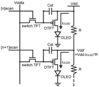
Fig. 1. Circuit scheme of the conventional pixel circuit (2T1C) and the voltage drop caused by the intrinsic parasitic resistance(R) at the V dd supply power line.
Fig. 2. (a) Proposed pixel design and timing scheme of the signal line. (b) Equivalent circuit at each stage in operation.
low to turn off T1, whereas scan[n] remains high. The source voltage of DTFT is discharged until it is turned off. This node voltage settles from V dd to V data+ V th, where V th is the threshold voltage of DTFT. Accordingly, the threshold voltage of DTFT and the data signal are stored in the right side of Cst. The left side of Cst is set to ground during stages (1) and (2). After the pixel scanning period, the third stage, which is the display period, is implemented. During stage (3), [n]scan is set to low to turn off T2 and T3 but turn on T4, and [n]EM is
set to high again so that the gate of DTFT can be connected to the left side of Cst; the source voltage of DTFT is charged up to V dd from V data+ V th. Immediately, the gate voltage of DTFT should be boosted to V dd− V data − V th by the conservation of charge in the capacitor as bootstrap is per-formed. Accordingly, DTFT starts to generate current(IOLED), which drives the OLED. Cst sustains the gate voltage of DTFT
V dd− V data − V th for the period of a frame. IOLEDis also the saturation current of DTFT. In this letter, the minimum design rule for the channel length of TFT devices is 5 µm, so that the second-order effect is not thereby considered in the proposed analysis. Thus,
IOLED= K[V gs − V th]2
= K [(V dd − V data − V th) − (V dd) − (−V th)]2 = K[V data]2.
Therefore, IOLED is independent of the threshold voltage of DTFT and the supply voltage and is affected only by data voltage.
III. SIMULATIONRESULTS
The HSPICE software with the Rensselaer Polytechnic Insti-tute (RPI) poly-Si TFT model(Level = 62) was used to verify the proposed circuit. The aspect ratio, mobility, and threshold voltage of DTFT were 3.3/5, 80 cm2/V· s, and −2 V. Cst was
set to 0.5 pF, V dd and the high level of the signals ([n]Scan and [n]EM) were set to 5 and 9 V, respectively. The initial supply voltage modulated such that the IOLEDin the following cases was approximately 1 µA as luminance and resolution were designed to be 300 cd/m2 and 133 ppi. From the 600 TFTs tested, the maximum shift of the threshold voltage is about 0.2 V at a mean threshold voltage of −2.41 V. In this letter, the variation of the threshold voltage of DTFT is set at 0.3 V to validate the worst case design.
Fig. 3(a) plots the simulation result of the proposed pixel structure when the threshold of the DTFT was set to−1.7, −2, and−2.3 V. The simulation results indicate that the variation of IOLED in the proposed pixel is clearly reduced using the adoption of the new threshold voltage compensation method. In a display period, the variation of IOLED in the proposed design is very small, which is between around 1.01 and 0.99 µA. Therefore, the strong immunity to the variation of the threshold voltage in the DTFT in the proposed pixel structure is verified. Fig. 3(b) shows that simulated degradation of the supply voltage on the panel is 0.5 V. According to Fig. 3(b), the deviation of IOLEDin the presented pixel structure is less than 2.5%, confirming the effectiveness of the prevention against the degradation of the supply voltage.
Fig. 4 shows the comparison of the IOLEDdegradation in the conventional pixel structure (2T1C) with that in the proposed structure (5T1C), which is caused by the drop in the supply voltage as the number of scan lines increases (240, 480, 600, 768) [11]. The x-axis indicates the distance from the supply voltage point to each pixel by the number of scan lines. By
LU et al.: ENHANCEMENT OF BRIGHTNESS UNIFORMITY FOR AMOLED DISPLAYS 745
Fig. 3. (a) Transient simulation results for the proposed pixel structure. With the threshold voltage shift of DTFT set as±0.3 V, the variation of output current is about 1.01−0.99 µA. (b) Transient simulation results for the proposed pixel structure. The deviation ofIOLEDin the proposed pixel structure is less than 2.5%, and the degradation of the supply voltage on the panel is 0.5 V.
Fig. 4. Comparison of nonuniformity of output current between the conven-tional pixel structure (2T1C) and the proposed one (5T1C) caused by the drop in supply voltage with an increasing number of scan lines (240, 480, 600, 768).
increasing the number of scan lines for large-size or high-resolution AMOLED displays, the resistance of the power line leads to the larger supply voltage drop in the conventional 2T1C pixel design. In contrast, in the proposed 5T1C pixel design, the
nonuniformity of the output current remains almost constant while the number of scan lines increases, and the maximum degradation of IOLED is just approximately 3.1%. Therefore, the proposed pixel structure is a promising candidate for use in large-size and high-resolution AMOLED displays.
IV. CONCLUSION
A new voltage modulation pixel circuit is developed for application to large-size and high-resolution AMOLED dis-plays. The nonuniformity of the output current is improved substantially using the proposed compensation operation. The average deviation of the TFT driving current is about 50 nA as the threshold voltage is varied by 0.3 V, and the nonuniformity of the IOLED with increasing number of scan lines in the proposed pixel structure is less than 3.1%. The simulation results successfully demonstrate that the proposed circuit has high immunity to both the voltage variation in poly-Si TFTs and the drop in the supply voltage.
ACKNOWLEDGMENT
The authors would like to thank AU Optronics Corporation and Dr. C. W. Chen for his discussions.
REFERENCES
[1] V. W. C. Chan, P. C. H. Chan, and C. Yin, “The effect of grain boundaries in the electrical characteristics of large grain polycrystalline thin-film transistor,” IEEE Trans. Electron Devices, vol. 49, no. 8, pp. 1384–1391, Aug. 2002.
[2] R. Dawson, Z. Shen, D. A. Furest, S. Connor, J. Hsu, M. G. Kane, R. G. Stewart, A. Ipri, C. N. King, P. J. Green, R. T. Flegal, S. Pearson, W. A. Tang, S. Van Slyke, F. Chen, J. Shi, M. H. Lu, and J. C. Sturm, “The impact of the transient response of organic light emitting diodes on the design of active matrix OLED displays,” in IEDM Tech. Dig., 1998, pp. 875–878.
[3] S. H. Jung, W. J. Nam, and M. K. Han, “A new voltage-modulated AMOLED pixel design compensating for threshold voltage variation in poly-Si TFTs,” IEEE Electron Device Lett., vol. 25, no. 10, pp. 690–692, Oct. 2004.
[4] T. Sasaoka, M. Sekiya, A. Yumoto, J. Yamada, T. Hirano, Y. Iwase, T. Yamada, T. Ishibashi, T. Mori, M. Asano, S. Tamura, and T. Urabe, “A 13.0-inch AMOLED display with top emitting structure and adaptive current mode programmed pixel circuit (TAC),” in Proc. SID Tech. Dig., 2001, pp. 384–387.
[5] J. C. Goh, C. K. Kim, and J. Jang, “A novel pixel circuit for active-matrix organic light-emitting diodes,” in Proc. SID Tech. Dig., 2003, pp. 494–497.
[6] Y. C. Lin and H. P. D. Shieh, “Improvement of brightness uniformity by AC driving scheme for AMOLED display,” IEEE Electron Device Lett., vol. 25, no. 11, pp. 728–730, Nov. 2004.
[7] J. C. Goh, H. J. Chung, J. Jang, and C. H. Han, “A new pixel circuit for active matrix organic light emitting diodes,” IEEE Electron Device Lett., vol. 23, no. 9, pp. 544–546, Sep. 2002.
[8] Y. H. Tai, B. T. Chen, Y. J. Kuo, C. C. Tsai, K. Y. Chiang, Y. J. Wei, and H. C. Cheng, “A new pixel circuit for driving organic light-emitting diode with low temperature,” J. Display Technol., vol. 1, no. 1, pp. 100–104, Sep. 2005.
[9] H. J. In, I. H. Jeong, J. S. Kang, O. K. Kwon, and H. K. Chung, “A novel feedback-type AMOLEDs driving method for large-size panel applica-tions,” in Proc. SID Tech. Dig., 2005, pp. 252–255.
[10] H. Miyake, Y. Yamazaki, J. Koyama, M. Hayakawa, M. Osame, S. Seo, and S. Yamazaki, “A voltage driving AMOLED display with luminance control,” in Proc. SID Tech. Dig., 2005, pp. 240–243.
[11] M. Stewart, R. S. Howell, L. Pires, M. K. Hatalis, W. Howard, and O. Prache, “Polysilicon VGA active matrix OLED displays—Technology and performance,” in IEDM Tech. Dig., 1998, pp. 871–874.