Enhanced Luminous Efficiency of WLEDs
Using a Dual-Layer Structure of the
Remote Phosphor Package
Kuo-Ju Chen, Hsin-Chu Chen, Min-Hsiung Shih, Member, IEEE, Chao-Hsun Wang, Hsin-Han Tsai,
Shih-Hsuan Chien, Chien Chung Lin, Member, IEEE, and Hao-Chung Kuo, Senior Member, IEEE
Abstract—This study demonstrates how the insertion of a
thin silicone layer into a dual-layer remote phosphor structure
enhances light extraction in white light-emitting diodes (WLEDs).
In the experiment, a dual-layer phosphor structure yielded a
higher intensity of blue and yellow components than a
conven-tional structure. Moreover, the lumen flux was 5% higher than
a conventional remote phosphor package at the same correlated
color temperature (CCT). Using a TFCalc32 simulation, the
electric field intensity was calculated for different thicknesses of
the dual-layer remote phosphor structures, and the enhanced use
of blue rays was verified. Additionally, the dual-layer structure
reduces chromaticity deviations as the driving current increases.
Index Terms—Coatings, GaN, light-emitting diodes,
optoelec-tronic devices, packaging, phosphor.
I. I
NTRODUCTIONP
HOSPHOR-CONVERTED white light-emitting diodes
(WLEDs) are a promising light source because of their
small size, high energy efficiency, low cost, and color stability
[1]–[4]. WLEDs apply the principle of complementary colors:
Blue light from a blue chip is combined with yellow light
from phosphor [5]. WLEDs have the potential to be used
in solid-state lighting, but their luminous efficiency must be
enhanced [6]. Generally, freely dispersed coating is the most
common method used to fabricate white light. In this process,
transparent encapsulated resin is combined with phosphor
powder and is dispersed on the phosphor package. Although
this approach allows the thickness of the phosphor layer to
Manuscript received December 02, 2012; revised February 07, 2013; accepted February 28, 2013. Date of publication May 03, 2013; date of current version May 27, 2013. This work was supported in part by the National Science Council in Taiwan under Grant NSC100-3113-E-009-001-CC2 and Grant NSC-99-2120-M-009-007.
K.-J. Chen, C.-H. Wang, S.-H. Chien, and H.-C. Kuo are with the Department of Photonics and Institute of Electro-Optical Engineering, National Chiao Tung University, Hsinchu 30010, Taiwan (e-mail: [email protected]).
H.-C. Chen is with the Department of Photonics and Institute of Electro-Op-tical Engineering, National Chiao Tung University, Hsinchu 30010, Taiwan. He is also with the Electronics and Optoelectronics Research Laboratories, Indus-trial Technology Research Institute, Hsinchu 30010, Taiwan.
M.-H. Shih is with the Department of Photonics and Institute of Electro-Op-tical Engineering, National Chiao Tung University, Hsinchu 30010, Taiwan. He is also with the Research Center for Applied Sciences, Academia Sinica, Taipei 115 Taiwan (e-mail: [email protected]).
C. C. Lin is with the Institute of Photonics System, National Chiao Tung University, Tainan 711, Taiwan.
Color versions of one or more of the figures in this paper are available online at http://ieeexplore.ieee.org.
Digital Object Identifier 10.1109/JLT.2013.2260322
be controlled easily and reduces much of the cost, it does not
produce high-quality WLEDs [7]. Therefore, the conformal
coating method can be used as an alternative. This method
distributes colors uniformly, resulting in angular homogeneity
of correlated color temperature (CCT) [8]. However, the
disad-vantage of a conformal phosphor structure is the backscattering
effect, which reduces luminous efficiency.
Previous studies have demonstrated the concept of separating
the chip and the phosphor layer of remote phosphor structures
[9], [10]. The enhanced light extraction internal reflection
(ELiXIR) structure, which uses a polymer hemispherical shell
lens with interior phosphor coating, is known to increase
extraction efficiency [11]. Furthermore, an air-gap embedded
structure can enhance luminous efficiency by reflecting
down-ward light [12].
In addition to the structure of the package, the concentration
of phosphor plays an important role on luminous efficiency. The
re-absorption loss in the phosphor layer raises when the
phos-phor concentration increases. Therefore device luminous
effi-ciency would be degraded, especially at lower CCTs [13].
Sim-ilarly, Narendran et al. demonstrated that high occurrence of
scattering and reflecting also reduces luminous efficiency [14].
Therefore, it is essential to enhance the emission of blue and
yellow rays and reduce the amount of light lost from
backscat-tering and reflection.
In this study, a dual-layer phosphor structure was employed
in a remote phosphor package to increase light output
com-pared to a conventional remote phosphor structure at the same
CCT. The experimental results indicate that a dual-layer
phos-phor structure yielded higher light transmission than a
conven-tional phosphor structure. Furthermore, a TFCalc32 simulation
demonstrated that the power intensity between the silicone layer
and the phosphor layers was enhanced. The chromaticity
coor-dinate deviations were also improved by increasing the driving
current of the LED.
II. E
XPERIMENTIn this experiment, a dual-layer structure was fabricated using
the pulse spray coating method, which creates a uniform
phos-phor layer [15]–[17]. The phosphos-phor powder was YAG:
with the particle size of 13
. An InGaN-based blue LED
with a peak emission wavelength of approximately 450 nm was
bonded on silver glue with gold wire in a lead-frame package.
The schematic cross-sectional view of a dual-layer remote
phos-phor structure is shown in Fig. 1. The samples were fabricated
Fig. 1. Schematic cross-sectional view of (a) dual-layer and (b) conventional remote phosphor structures.
by the following steps: First, the silicone encapsulant was filled
in a commercial plastic lead-frame package.
The pulse spray coating method was then employed to spray
phosphor and silicone binder on the surface of each layer of the
remote phosphor structure. Finally, phosphor was sprayed on
top of the remote phosphor structure to obtain the same CCT as
the conventional remote phosphor structure. In the experiment,
the total density of the phosphor in the experiment is set up as
6
for all the samples and the density of phosphor is
approximately 1.0 mg/cm2 from one spray coating step. To
ob-tain the better luminous efficiency of the devices, the thickness
of the top and bottom phosphor layers was adjusted. Thus, the
ratio of the sample A, B, and C represent the different density
of phosphor layer in the dual-layer structure.
III. R
ESULTS ANDD
ISCUSSIONThe effect of changing the ratios of the first and the second
layers of the phosphor structure is shown in Fig. 2(a), which
represents the transmission of the different samples in relation
to the wavelength. The remote phosphor package composed of
a dual-layer structure yielded the highest transmission at
wave-lengths ranging from 400 to 800 nm. The sample containing
the optimized ratio, Sample C, produced greater transmission
than the other samples in the experiment. Enhanced
transmis-sion means that the LED device emits more photons, reducing
light reflection and increasing light output.
The drop in intensity at a wavelength of 460 nm can be
attributed to the absorption of phosphor. Fig. 2(b) shows a
comparison of the lumen enhancement of the different
sam-ples. Sample C exhibits a 5% lumen enhancement over the
conventional remote phosphor structure. The transmission
measurement verified that this was the result of increased
extraction of rays in the yellow band. Therefore, increasing
light extraction is critical to improving the luminous efficiency
of LED structures.
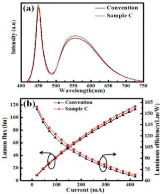
The emission spectra of Sample C and the conventional
re-mote phosphor structure are shown in Fig. 3(a). These
struc-tures had the same CCT at approximately 5400 K, and both
op-erated at a current of 120 mA. The dual-layer structure produced
a higher intensity in blue and yellow components and yielded
a higher light output than the conventional structure. Fig. 3(b)
shows the luminous flux and the luminous efficiency of both
Sample C and the conventional remote phosphor structure, each
driven at currents from 20 to 420 mA. Since the optical trapping
in the phosphor layer degrades device luminous efficiency due
Fig. 2. (a) The transmission of the different ratios of phosphor layers as wave-length increases (b) The lumen enhancement of the amount of phosphor in the second layer under the regular operation current.
Fig. 3. (a) The emission spectra (b) Luminous flux and luminous efficiency of the dual-layer and the conventional remote phosphor structures driven at cur-rents from 20 to 420 mA.
to the self-absorption of phosphor [18]. Comparing to the
refer-ence structure (the single-layer structure), the dual-layer
struc-ture can reduce the optical trapping of the phosphor layer, and
increase luminous flux.
In general, yellow rays scatter in all directions when pumped
by a blue ray. Consequently, most of the downward rays are lost
Fig. 4. Thickness-dependent of (a) the dual-layer and (b) the conventional LEDs by TFCalc32 simulation.
in the package and light output is reduced. Conversely, in the
dual-layer phosphor structure, a thin silicone layer with a low
refractive index is inserted into the phosphor layer. The
refrac-tive indices of the phosphor and silicone encapsulants used in
this study were 1.8 and 1.4, respectively.
According to Snell’s law, the total reflection angle needed
to be increased because of the phosphor/encapsulant layer.
Re-flecting the blue ray could improve its use because it increases
the probability of phosphor excitation [12]. Therefore, a
TF-Calc32 simulation was employed to observe the actual effect
of blue photons coupling to the phosphor layer.
In the simulation, the lengths of the first and second silicone
layers were approximately 850
and 70
, respectively.
The lengths of the first and second phosphor layers were
ap-proximately 100
and 20
, respectively. Regarding the
conventional phosphor structure, the silicone layer was
approx-imately 850
, and the phosphor layer was roughly 120
.
These layers were simultaneously subjected to 450 nm light by a
GaN LED. The results of this simulation are displayed in Fig. 4,
which shows the electric field intensity for the different
thick-nesses of dual-layer and conventional phosphor structures. The
electric field intensity in the second silicone layer was higher
than in the conventional phosphor structure. Therefore, the
ad-vantage of the former structure is that the incident blue ray can
be trapped in the lower refractive index medium, increasing the
absorption ability of the phosphor layer and transferring more
yellow rays than the conventional structure.
The power intensity of dual-layer and conventional remote
phosphor structures in WLEDs can be calculated as shown in
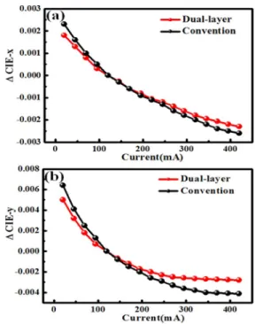
Fig. 5. The chromaticity deviations of (a) CIE coordinate and (b) CIE coordinate with dual-layer and conventional remote phosphor structures at dif-ferent LED injection currents.
(1)–(2) at the bottom of the page, where
and
are the
re-fractive indices silicone and phosphor, and
is the electric
field intensity.
According to (1) and (2), the power intensities of the
dual-layer and conventional remote phosphor structures were 20.2%
and 13.8%, respectively, at a wavelength of 450 nm.
Further-more, the power intensity reached a maximum of 46.4%, an
en-hancement that mainly occurred between the thin silicone layer
and the phosphor layers. The enhanced electric field intensity
allows more blue rays to be trapped and raises the probability
of phosphor excitation. In turn, this recycling of photons allows
for the production of more yellow rays.
Fig. 5 shows the chromaticity deviations of (a) CIE
co-ordinate and (b) CIE
coordinate with dual-layer and
con-ventional remote phosphor structures from 20 to 420 mA, the
light quality of the dual-layer and conventional remote
phos-phor structures can be compared. As the current increased,
inci-dent blue rays were generated from the blue chip and converted
the phosphor layer to yellow photons. Therefore, the manner in
which the phosphor layer is used determines the quality of color
mixing in WLEDs, especially at different currents. The
lowest-(1)
rents. Therefore, the dual-layer remote phosphor structure not
only enhanced the luminous flux of the WLED, but also
pro-vided greater stability of CIE coordinates as the driving current
increased.
IV. C
ONCLUSIONThis study demonstrates that a dual-layer remote phosphor
structure enhances the luminous efficiency of WLEDs. Inserting
a thin silicone layer into the phosphor layer and optimizing the
ratio of the different layers increased transmission, thereby
in-creasing light output. Moreover, TFCalc32 simulation results
verified that more incident blue rays were reflected in the thin
silicone layer of the dual-layer structure, increasing the
proba-bility of phosphor excitation and producing higher yellow
com-ponents in the emission spectra. Accordingly, the luminous flux
of the dual-layer structure was 5% higher than that of the
con-ventional remote phosphor package at a driving current of 120
mA. Finally, the dual-layer structure reduces chromaticity
de-viations as the driving current increases. These results establish
WLEDs as a capable source of solid-state lighting.
A
CKNOWLEDGMENTThe authors would like to thank Helio Opto., and
Hermes-Epitek Corp., for their technical support.
R
EFERENCES[1] S. Nakamura, T. Mukai, and M. Senoh, “Candela-class high-brightness InGaN/AlGaN double-heterostructure blue-light-emitting diodes,” Appl. Phys. Lett., vol. 64, no. 13, pp. 1687–1689, 1994.
[2] E. F. Schubert and J. K. Kim, “Solid-state light sources getting smart,” Sci., vol. 308, no. 5726, pp. 1274–1278, 2005.
[3] S. Pimputkar, J. S. Speck, S. P. DenBaars, and S. Nakamura, “Prospects for LED lighting,” Nat. Photon., vol. 3, no. 4, pp. 179–181, 2009. [4] H. T. Huang, Y. P. Huang, and C. C. Tsai, “Planar lighting system using
array of blue LEDs to excite yellow remote phosphor film,” J. Display Technol., vol. 7, no. 1, pp. 44–51, 2011.
[5] H. K. Park, J. H. Oh, and Y. R. Do, “Toward scatter-free phosphors in white phosphor-converted light-emitting diodes,” Opt. Exp., vol. 20, no. 9, pp. 10218–10228, 2012.
[6] S. Yun, Y. He, N. T. Tran, and F. G. Shi, “Angular CCT uniformity of phosphor converted white LEDs: Effects of phosphor materials and packaging structures,” IEEE Photon. Technol. Lett., vol. 23, no. 3, pp. 137–139, 2011.
[7] M. R. Krames, O. B. Shchekin, R. Mueller-Mach, G. O. Mueller, L. Zhou, G. Harbers, and M. G. Craford, “Status and future of high-power light-emitting diodes for solid-state lighting,” J. Display Technol., vol. 3, no. 2, pp. 160–175, 2007.
[8] H. T. Huang, C. C. Tsai, and Y. P. Huang, “Conformal phosphor coating using pulsed spray to reduce color deviation of white LEDs,” Opt. Exp., vol. 18, no. 13, pp. A201–A206, 2010.
[9] H. Luo, J. K. Kim, E. F. Schubert, J. Cho, C. Sone, and Y. Park, “Anal-ysis of high-power packages for phosphor-based white-light-emitting diodes,” Appl. Phys. Lett., vol. 86, no. 24, p. 243505, 2005. [10] J. K. Kim, H. Luo, E. F. Schubert, J. H. Cho, C. S. Sone, and Y. J. Park,
“Strongly enhanced phosphor efficiency in GaInN white light-emitting diodes using remote phosphor configuration and diffuse reflector cup,” Jpn. J. Appl. Phys., vol. 44, no. 20, pp. L649–L651, 2005.
[11] S. C. Allen and A. J. Steckl, “ELiXIR – Solid-state luminaire with enhanced light extraction by internal reflection,” J. Display Technol., vol. 3, no. 2, pp. 155–159, 2007.
[12] H. C. Chen, K. J. Chen, C. C. Lin, C. H. Wang, C. C. Yeh, H. H. Tsai, M. H. Shih, and H. C. Kuo, “Improvement of lumen efficiency in white light-emitting diodes with air-gap embedded package,” Microelectron. Reliab., vol. 52, no. 5, pp. 933–936, 2012.
Stat. Sol (a), vol. 202, no. 6, pp. 60–62, 2005.
[15] H. C. Kuo, C. W. Hung, H. C. Chen, K. J. Chen, C. H. Wang, C. W. Sher, C. C. Yeh, C. C. Lin, C. H. Chen, and Y. J. Cheng, “Patterned structure of REMOTE PHOSPHOR for phosphor-converted white LEDs,” Opt. Exp., vol. 19, no. 14, pp. A930–A936, 2011.
[16] H. C. Chen, K. J. Chen, C. C. Lin, C. H. Wang, H. V. Han, H. H. Tsai, H. T. Kuo, S. H. Chien, M. H. Shih, and H. C. Kuo, “Improvement in uniformity of emission by nano-particles for white LEDs,” Nanotechnology, vol. 23, no. 26, p. 265201, 2012.
[17] K. J. Chen, H. C. Chen, K. A. Tsai, C. C. Lin, H. H. Tsai, S. H. Chien, B. S. Cheng, Y. J. Hsu, M. H. Shih, C. H. Tsai, H. H. Shih, and H. C. Kuo, “Resonant-enhanced full-color emission of quantum-dot-based display technology using a pulsed spray method,” Adv. Funct. Mater., vol. 18, pp. A201–A206, 2010.
[18] N. T. Tran and F. G. Shi, “Studies of phosphor concentration and thickness for phosphor-based white light-emitting-diodes,” J. Lightw. Technol., vol. 26, no. 21, pp. 3556–3559, 2008.
Kuo-Ju Chen was born in Taichung, Taiwan, R.O.C. He received a B.S degree
in industry education from National Kaohsiung Normal University (NKNU), Kaohsiung, Taiwan, in 2008, and his M.S. degree from National Taiwan Normal University (NTNU). He is currently pursuing a Ph.D. degree at National Chiao-Tung University, Hsinchu, Taiwan.
His focus is on UV excitable phosphate, which has high luminous efficiency and high stability. He used the combinatorial chemistry to develop UV-excited phosphor for his master thesis. His Ph.D. research includes fabrication, simula-tion, and characterization for high-power light-emitting diodes.
Hsin-Chu Chen was born in Miaoli, Taiwan, R.O.C., in 1981. He received a
Ph.D. degree at Institute of Electro-Optical Engineering, National Chiao Tung University, Taiwan, in 2012. His thesis work focused on quantum dots and the nanostructure with optoelectronics devices, which includes fabrication, simula-tion, and measurement. Since 2013, he has been at Industrial Technology Re-search (ITRI) in Hsinchu, Taiwan, where he holds an engineer. He has been working for the development of high color uniformity and high lumen efficiency of white light LED devices, which includes structure design, fabrication, simu-lation, and measurement.
Min-Hsiung Shih received B.S degree in physics from the National Cheng
Kung University, Tainan, Taiwan, in 1995, the M.S. degree in physics from the National Tsing Hua University (NTHU), Taiwan in 1997, and the Ph.D. degree in electrical engineering/electrophysics from the University of Southern Cali-fornia (USC), Los Angeles, in 2006.
He is current an associate research fellow in the Research Center for Ap-plied Sciences (RCAS), Academia Sinica, Nankang, Taiwan. He has authored more than 50 journal and conference publications. His research interests include integrated photonic circuits, photonic crystals, GaN based lasers, surface plas-monics, and cavity quantum electrodynamics.
Chao-Hsun Wang received his B.S. and M.S. degrees from the Department
of Photonics at National Chiao-Tung University, Hsinchu, Taiwan, in 2008 and 2009, respectively. He is currently working toward a Ph.D. degree in the De-partment of Photonics, National Chiao-Tung University. His current research interests include the efficiency droop behavior in GaN-based LEDs and high lumen efficiency white LEDs.
Hsin-Han Tsai is currently a master’s candidate in the Institute of
Electro-Op-tical Engineering, National Chiao Tung University, Taiwan. His focus is on white light LED packaging, which can improve angular-dependent CCT unifor-mity and enhance light output. His master’s research includes white light LED packaging, simulation, and measurement.
Shih-Hsuan Chien was born in Taoyuan, Taiwan, ROC. He received the B.S
degree in National Chiao-Tung University(NCTU), HsinChu, Taiwan, in 2012. He is currently pursuing an M.S. degree at National Chiao-Tung University, Hsinchu, Taiwan. His master’s focus is on high-powered white light-emitting diodes, including fabrication, simulation, measurement, and optical character-istic study. In addition, he researches optical applications of a promising mate-rial quantum dot.
Chien-Chung Lin (S’93–M’02) was born in Taipei, Taiwan, R.O.C., in 1970.
He received a B.S. degree in electrical engineering from National Taiwan Uni-versity in 1993, and his M.S. and Ph.D. degrees in electrical engineering from Stanford University, Stanford, CA, in 1997 and 2002, respectively. His thesis work focused on design, modeling, and fabrication of micromachined tunable optoelectronic devices. Since 2009, he has been at National Chiao-Tung Univer-sity (NCTU) in Tainan, Taiwan, where he holds a position as assistant professor. The major research efforts in his group are in the design and fabrication of semi-conductor optoelectronic devices, including LEDs, solar cells, and lasers. Be-fore joining NCTU, he worked for different start-ups in the United States. After graduating from Stanford in 2002, he joined E2O Communications, Inc, in Cal-abasas, California, as a senior optoelectronic engineer. His main research in-terests then were in optically and electrically pumped long-wavelength vertical cavity surface emitting lasers. In 2004, he joined Santur Corporation in Fre-mont California, where he initially worked as a member of technical staff and then became Manager of Laser Chip Engineering. He had worked on various projects such as monolithic multi-wavelength DFB Laser arrays for data and telecommunications applications, yield and reliability analysis of DFB Laser arrays, and so on. Dr. Lin has more than 30 journal and conference publications and is a member of the IEEE Photonic Society and Electron Devices Society.
Hao-Chung Kuo (S’98–M’99–SM’06), received a B.S. degree in physics from
National Taiwan University, Taiwan, R.O.C., an M.S. degree in electrical and computer engineering from Rutgers University, New Brunswick, NJ, in 1995, and his Ph.D. degree from the Electrical and Computer Engineering Depart-ment, University of Illinois at Urbana Champaign, in 1999. He has an extensive professional career both in research and industrial research institutions that in-cludes being a Research Consultant in Lucent Technologies, Bell Laboratories (1993–1995); and a Member of Technical Staff in Fiber-Optics Division at Ag-ilent Technologies (1999–2001) and LuxNet Corporation (2001–2002). Hong Kong ASTRI (2004). Since October 2002, he has been with National Chiao Tung University as a Faculty Member of the Institute of Electro-Optical Engi-neering. He is now the Chairman of the Department of Photonics and Institute of Electro-Optical Engineering, NCTU. His current research interests include semiconductor lasers, VCSELs, blue and UV LED lasers, quantum-confined op-toelectronic structures, opop-toelectronic materials, and solar cells. He has authored and coauthored 200 SCI journal papers, 200 conference papers, and 8 granted and 14 pending patents. Prof. Kuo is an IEEE Senior member and Assoc. Editor of IEEE/OSA J. of Lightwave Technology and JSTQE-special issue Solid State Lighting. He received the Ta-You Wu Young Scholar Award from the National Science Council and the Young Photonics researcher award in 2007. He was elected as OSA fellow in 2012.