Electrical properties of Ta 2 O 5 thin films deposited on Ta
S. Ezhilvalavan and Tseung-Yuen Tseng
Citation: Applied Physics Letters 74, 2477 (1999); doi: 10.1063/1.123013 View online: http://dx.doi.org/10.1063/1.123013
View Table of Contents: http://scitation.aip.org/content/aip/journal/apl/74/17?ver=pdfcov
Published by the AIP Publishing
Articles you may be interested in
Effects of postannealing on the electrical properties of Ta 2 O 5 thin films deposited on TiN/T
J. Appl. Phys. 88, 7242 (2000); 10.1063/1.1326464
Defect dominated charge transport in amorphous Ta 2 O 5 thin films
J. Appl. Phys. 88, 850 (2000); 10.1063/1.373747
Electrical characteristics of Ta 2 O 5 thin films deposited by electron beam gun evaporation
Appl. Phys. Lett. 75, 2836 (1999); 10.1063/1.125166
The effect of Al – Ta 2 O 5 topographic interface roughness on the leakage current of Ta 2 O 5 thin films
Appl. Phys. Lett. 74, 2800 (1999); 10.1063/1.124018
Effect of bismuth content on the properties of Sr 0.8 Bi x Ta 1.2 Nb 0.9 O 9+y ferroelectric thin films
J. Appl. Phys. 85, 1095 (1999); 10.1063/1.369234
This article is copyrighted as indicated in the article. Reuse of AIP content is subject to the terms at: http://scitation.aip.org/termsconditions. Downloaded to IP: 140.113.38.11 On: Thu, 01 May 2014 08:42:29
Electrical properties of Ta
2O
5thin films deposited on Ta
S. Ezhilvalavan and Tseung-Yuen Tsenga)Department of Electronics Engineering and Institute of Electronics, National Chiao–Tung University, Hsinchu-300, Taiwan, Republic of China
~Received 19 October 1998; accepted for publication 4 March 1999!
The electrical properties of reactively sputtered Ta2O5thin films with Ta as the bottom electrodes
were investigated. Ta films were deposited onto SiO2/n-Si substrates by sputtering in Ar and in situ
annealed at 700 °C for 10 min in N2 at a chamber pressure of 20 mTorr. We compared the
effectiveness of both as-deposited and annealed Ta bottom electrodes on the leakage characteristics of Ta2O5 thin films. We also envisaged the influence of the surface roughness and morphology of
the Ta bottom electrode in modifying the resultant microstructure of the annealed Ta2O5 films.
Present studies demonstrate the use of Ta as a potential bottom electrode material to replace the precious metal electrodes and to simplify the fabrication process of the Ta2O5 storage capacitor.
© 1999 American Institute of Physics.@S0003-6951~99!03317-3#
Tantalum pentoxide (Ta2O5) has been practically the most promising capacitor material to be used in the near future dynamic random access memories~DRAMs!, because of its high dielectric constant, thermal and chemical stability, and good step coverage.1,2 As the DRAM generation goes 256 M-bit and beyond, the DRAM fabrication process has become more and more complicated. This will cause the pro-duction cost of the high density DRAMs unacceptably high and will significantly degrade the device reliability. Thus, it is essential to develop a process technology that is simple and yet ensures high performance and high reliability.3 Cur-rent semiconductor technology demands the use of low-resistivity metals as electrode materials for ultralarge scale integrated~ULSI! conduction lines and contact structures. In order for ULSI circuits manufacturing to minimize the cost of ownership aspect in the metallization process, several metallization technologies have been proposed. The eviden-tial criteria in choosing the most probable are physical or material limitations ~e.g., step coverage and resistivity! and manufacturing requirements such as process complexity, re-liability, throughput, and total cost. Replacing the precious metals with a base metals like Al and Ni have been at-tempted in the mass production of multilayer ceramic chip capacitors.4 More recently we have reported the electrical properties of Ta2O5thin films deposited on Cu.
5
Al, Ni, and Cu electrodes are easily oxidized during deposition ~sputter-ing! or in the annealing process. Consequently, annealing in low oxygen partial pressure ( p-O2) is indispensable and may
cause the formation of oxygen vacancies in the ceramic bod-ies of the capacitors.
There have been several technical problems associated with the Ta2O5films during the high temperature processing
steps, necessary for their applicability to integrated circuits, which cause significant increase of the leakage current. This, obviously, limits their use in DRAMs in terms of the refresh characteristics of the cell. Another problem associated with Ta2O5 is the choice of bottom electrode. Usually poly-Si is
used as the bottom electrode. However, since Si has stronger
electron affinity than Ta, poly-Si cannot be used as the bot-tom electrode. The oxide materials deposited onto the Si ~metal–oxide–semiconductor structure! cause interaction or atomic interdiffusion with Si at elevated temperatures which result in the formation of a lower dielectric constant interfa-cial layer of silicon oxide.6This problem becomes quite se-vere as the oxide thickness is reduced into the sub-micron range. The alternative is the use of a metal–semiconductor– metal ~MIM! structure, i.e., to deposit the dielectric film on an intermediate base electrode which remain electrically con-ductive after exposure to an oxidizing environment at high temperatures. The bottom metal electrode layer also prevent the interdiffusion of silicon or oxygen across the interface, thus eliminating the formation of an undesirable interfacial layers. Ta metal can be adopted as the bottom electrode be-cause it is thermodynamically and electrically compatible with Ta2O5 and it has excellent barrier property against
diffusants.7,8Another advantage is the simplicity of the pro-cessing techniques, i.e., the dielectric film and the bottom electrode can be in situ made using the same target material and in a single sputtering machine followed by in situ an-nealing processing without being exposed to outside atmo-spheres, thereby avoids contamination if any, in between the processing steps. In this letter we report the preliminary ex-perimental results of the effect of Ta as a bottom electrode material on the electrical and dielectric properties of reac-tively sputtered Ta2O5thin films for the first time. The
stud-ies show the high reliability and quality of the Ta2O5film for
the possible integration into ULSI applications.
The n-type silicon wafer was cleaned by a standard cleaning process. The Ta bottom electrode on SiO2/n-Si
substrate with a thickness of 100 nm was deposited by direct current-magnetron sputtering from a high purity tantalum metal target ~2.5 in. in diameter!. The Ta film was prepared at a fixed power of 35 mW and at a constant pressure of 10 mTorr with Ar as the sputtering gas. The as-deposited Ta bottom layer was in situ annealed at 700 °C/10 min in N2at
a chamber pressure of 20 mTorr. Ta2O5films were deposited
on to the Ta/SiO2/n-Si bottom storage node electrode in the
same sputtering machine without breaking the vacuum. The
a!Electronic mail: [email protected]
APPLIED PHYSICS LETTERS VOLUME 74, NUMBER 17 26 APRIL 1999
2477
0003-6951/99/74(17)/2477/3/$15.00 © 1999 American Institute of Physics This article is copyrighted as indicated in the article. Reuse of AIP content is subject to the terms at: http://scitation.aip.org/termsconditions. Downloaded to IP:
sputtering gas consists of 80% Ar and 20% O2mixture with
a total pressure of 10 mTorr. More details on the deposition technique may be found in Refs. 5 and 6. Film thickness was estimated to be 100 nm by using a Tencor Alpha-step 200 profilometer. The rapid thermal annealing ~RTA! of the Ta2O5 film was performed, before patterning the top elec-trode in a RTA furnace ~Ulvac Sinku-Rico, HPC 700! at 800 °C for 30 s in O2ambient. The RTA process temperature
~800 °C! and annealing time ~30 s! were chosen based on our earlier study.9The heating rate used was the maximum heat-ing rate of about 100 °C/s. The Pt top electrode with a thick-ness of 100 nm and diameters of 150, 250, and 350mm were patterned by a shadow mask process. The current–voltage (I – V) characteristics of the Ta2O5 films were measured on
the MIM structure with a delay time of 30 s using HP4145B semiconductor parameter analyzer. The capacitance–voltage (C – V) characteristic and the dielectric loss tangent were recorded at frequencies ranging from 100 Hz to 10 MHz with 0.5 V alternating current ~ac! sweeping signal using HP4194A impedance-gain phase analyzer.
Four probe resistivity measurement and x-ray diffraction @~XRD!, Model D5000, Siemens, Munich, FRG# were em-ployed to identify the Ta and Ta2O5 phases of the sputtered
films. The structure of the as-deposited Ta film on SiO2/n-Si
substrate is amorphous. However, Ta crystallizes after in situ annealing at 700 °C for 10 min in N2atmosphere inside the
sputtering chamber, keeping the total pressure of about 20 mTorr. The resulting phase is identified asb-Ta~tetragonal! as shown in Fig. 1~a!, with a resistivity of ;175 mV cm. Resistivity of the order of 30mV cm or less were indicative of body-centered-cubic-Ta, while 160–200mV cm was char-acteristic of b-Ta.7,8,10 Detailed studies of XRD of Ta2O5 films deposited on as-deposited and in situ annealed Ta bot-tom electrode were carried out. The results showed that as-deposited Ta2O5 films were amorphous and the annealed
Ta2O5 films crystallized into b-Ta2O5 ~orthorhombic!
irre-spective of whether the bottom Ta electrode is amorphous or crystallized~b-Ta! @Fig. 1~b! and 1~c!#. In addition, it is to be noted that annealed Ta2O5 films exhibit a very strong
pre-ferred orientation i.e., peaks of certain reflections of the dif-fracting planes dominate the XRD pattern. The intensities of
the ~001! and ~002! reflections dominate in the annealed Ta2O5 films deposited on the as-deposited amorphous Ta
whereas ~1 11 0! and ~1 11 1! became predominant in the Ta2O5films deposited on the annealed crystallized Ta bottom
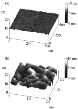
electrode. The earlier results demonstrate that the structure of the Ta bottom electrode and its surface morphology has sig-nificant influence on the crystallographic orientation of the deposited films. To elucidate this, the root-mean-square ~rms! surface roughness and morphology of the as-deposited and annealed films were examined using atomic force mi-croscopy@~AFM!, Digital Instruments, Nano-Scope III#. The rms surface roughness of the as-deposited Ta bottom layer is ;0.315 nm, whereas the annealed Ta bottom electrode show a decreased rms value of ;0.249 nm. Compared to the an-nealed Ta2O5 film deposited on as-deposited Ta, the film sputtered on the annealed Ta electrode was having higher rms value i.e., the rms value increased from 0.277 to 1.394 nm ~Fig. 2!. The larger rms surface roughness of the an-nealed Ta2O5 films on the annealed Ta bottom electrode is probably due to the crystallization and grain growth of the bottom electrode itself.11
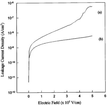
The important electrical characteristics of the dielectric material to be used as storage capacitors in DRAMs is the low leakage current density and reasonable high dielectric constant. Figure 3 shows the leakage current density versus electric field for the annealed Ta2O5 thin films deposited on
the as-deposited Ta~a! and annealed Ta bottom electrode ~b!. Results in this study demonstrate that the Ta2O5 thin film
deposited on the annealed Ta bottom electrode exhibit lower leakage current density of about 1029A/cm2 at an applied field of 100 kV/cm. The difference in the leakage character-istics of the Ta2O5 film with respect to the as-deposited
against the annealed Ta bottom electrode may be attributed to the effective reduction of oxygen vacancies through the grain boundaries of annealed Ta electrode. Although
scan-FIG. 1. XRD spectra of Ta and 30 s 800 °C O2RTA processed Ta2O5films:
~a! Ta film in situ annealed at 700 °C for 10 min in N2, ~b! Ta2O5film
sputtered on the as-deposited Ta, and~c! Ta2O5deposited on the annealed
Ta bottom electrodes.
FIG. 2. AFM images of the RTA processed Ta2O5film deposited on~a!
as-deposited Ta and~b! annealed Ta bottom electrodes.
2478 Appl. Phys. Lett., Vol. 74, No. 17, 26 April 1999 S. Ezhilvalavan and T.-Y. Tseng
This article is copyrighted as indicated in the article. Reuse of AIP content is subject to the terms at: http://scitation.aip.org/termsconditions. Downloaded to IP: 140.113.38.11 On: Thu, 01 May 2014 08:42:29
ning electron microscope~Model S2500, Hitachi, Japan! ob-servations indicate that both annealed Ta2O5films deposited
on the as-deposited and annealed Ta bottom electrodes ex-hibit smaller grain size distribution <1 nm, larger grain boundary regions are distinctly visible in the case of Ta2O5
films deposited on annealed crystallized Ta bottom electrode. Root-mean-square surface roughness and morphology obser-vations as shown in Fig. 2 also supports this results. These resultant grain and grain boundary modifications of the an-nealed Ta2O5film may be resulted from the nature of surface
conditions of the Ta bottom electrode on which the Ta2O5
film growth has taken place. That is, the crystallized Ta bot-tom electrode acts as an nucleation center for the large grain growth of the Ta2O5 films in comparison to the growth on
the as-deposited Ta bottom layer. During RTA processing, the O2 gas is decomposed into atomic oxygen (O*).12 The atomic oxygen will be absorbed on the surface of the film and then diffused into the film, more easily through grain boundary defects. Since the atomic oxygen is a strong oxi-dizing agent, it is believed that O*will participate the reduc-tion of defects of oxygen vacancies.
The dielectric constants of the Ta2O5 films were
calcu-lated from the accumulation capacitance at 100 kHz, the known area of the Pt electrodes of MIM capacitor and the ellipsometrically determined oxide thickness. The dielectric constants and the loss tangents of the Ta2O5films deposited
on the as-deposited and annealed Ta-bottom electrode are 35, 41, 0.02, and 0.03, respectively. Capacitance dispersion as a function of frequency from 100 Hz to 10 MHz were also studied to estimate the defect density contribution on the relaxation, and hence, its influence on the electrical proper-ties. There are at least four possible defects namely, the in-terface defect, grain boundary defect, shallow trap levels, and oxygen vacancies, may often exist in the MIM capaci-tors lead to a dielectric relaxation as a function of frequen-cies. The grain boundary and the interface defect are consid-ered to be a donor when it becomes neutral or positive by
donating an electron. When an ac voltage is applied, the defect levels move up or down with respect to the conduc-tion bands while the Fermi level remains fixed. A change of charge in the defect occurs when it crosses the Fermi level. Therefore, the defect density calculations can be done from the measurement of the real capacitance ~C! and the imagi-nary part of the capacitance (C*) as a function of frequency. Once C* is known, the defect density can be obtained from the relation Ddf5C*/qA, where A is the metal plate area and
q is the elemental charge.13The defect density of Ta2O5thin
films deposited on annealed Ta bottom electrode is 7.37 31010cm22V21, which is two orders smaller than that is
observed in perovskite based dielectric films such as Ba(12x)SrxTiO3 which exhibit significant dielectric
relax-ation at higher frequencies.14 From the capacitance disper-sion studies, we envisage that the dielectric relaxation of Ta2O5films on Ta is less pronounced and it has least
contri-bution from the defects, yet preserving lower leakage current density.
Time-dependent dielectric breakdown~TDDB! is a char-acteristic of the intrinsic materials, the method of processing, and electrode materials. TDDB studies demonstrate that Ta2O5 MIM films with Ta as the bottom electrode can also
survive the 10 years life time at a stress field of >700 kV/ cm. We have therefore, successfully demonstrated the effec-tive use of Ta as a possible bottom electrode material replac-ing the conventional precious metal electrodes for Ta2O5film
storage capacitors. Usage of Ta as an electrode will signifi-cantly reduce process complexity and the production cost of future high density DRAMs.
The authors gratefully appreciate the financial support from the National Science Council of Republic of China un-der Project No. NSC 87-2218-E 009-008.
1
S. Kamiyama, H. Suzuki, H. Watanabe, A. Sakai, M. Oshida, T. Tatsumi, T. Tanigawa, N. Kasai, and A. Ishitani, Tech. Dig. Int. Electron Devices Meet., 49~1993!.
2
Y. Ohji, Y. Matsui, T. Itoga, M. Hirayama, Y. Sugawara, K. Torii, H. Miki, M. Nakata, I. Asano, S. Iijima, and Y. Kawamoto, Tech. Dig. Int. Electron Devices Meet., 111~1995!.
3S. Ezhilvalavan and T. Y. Tseng, J. Mater. Science: Mater. Electron.~in
press!.
4S. Sumita, M. Ikeda, Y. Nakano, K. Nishiyama, and T. Nomura, J. Am.
Ceram. Soc. 74, 2739~1991!.
5
S. Ezhilvalavan and T. Y. Tseng, Thin Solid Films~submitted!.
6S. Ezhilvalavan and T. Y. Tseng, J. Appl. Phys. 83, 4797~1998!. 7K. Holloway and P. M. Fryer, Appl. Phys. Lett. 57, 1736~1990!. 8K. Holloway, P. M. Fryer, C. Cabral, Jr., J. M. E. Harper, P. J. Bailey, and
K. H. Kelleher, J. Appl. Phys. 71, 5433~1992!.
9
S. Ezhilvalavan and T. Y. Tseng, J. Am. Ceram. Soc. 82, 600~1999!.
10L. G. Feinstein and R. D. Huttemann, Thin Solid Films 16, 129~1973!. 11
M. S. Tsai, S. C. Sun, and T. Y. Tseng, J. Am. Ceram. Soc. 82, 351 ~1999!.
12W. S. Lau, P. W. Qian, N. P. Sandler, K. A. McKinley, and P. K. Chu,
Jpn. J. Appl. Phys., Part 1 36, 661~1997!.
13S. M. Sze, Physics of Semiconductor Devices, 2nd ed.~Wiley, New York,
1981!, p. 380.
14M. S. Tsai and T. Y. Tseng, Mater. Chem. Phys. 57, 47~1998!.
FIG. 3. Current–voltage characteristics of RTA processed Ta2O5films
de-posited on~a! as-deposited Ta and ~b! annealed Ta bottom electrodes.
2479 Appl. Phys. Lett., Vol. 74, No. 17, 26 April 1999 S. Ezhilvalavan and T.-Y. Tseng
This article is copyrighted as indicated in the article. Reuse of AIP content is subject to the terms at: http://scitation.aip.org/termsconditions. Downloaded to IP: 140.113.38.11 On: Thu, 01 May 2014 08:42:29