國 立 交 通 大 學
電 子 工 程 學 系 電 子 研 究 所 碩
士 班
碩 士 論 文
H.264解碼器之資料交換層級系統模擬
Transaction Level Modeling of H.264 Decoder
研 究 生:陳治傑
指導教授:蔣 迪 豪 博士
ii
Transaction Level Modeling of H.264 Decoder
研 究 生:陳治傑 Student: Chih-Chieh Chen
指導教授:蔣 迪 豪 博士 Advisor: Dr. Tihao Chiang
國立交通大學
電子工程學系 電子研究所碩士班
碩士論文
A Thesis
Submitted to Department of Electronics Engineering & Institute of Electronics College of Electrical and Computer Engineering
National Chiao-Tung University in Partial Fulfillment of the Requirements
for the Degree of Master in
Electronics Engineering June 2006
Hsinchu, Taiwan, Republic of China
iii
H.264解碼器之資料交換層級系統模擬
研究生:陳治傑 指導教授:蔣 迪 豪 博士 國立交通大學 電子工程學系 電子研究所碩士班摘 要
本篇論文中,我們介紹了一個在由上至下的設計流程中新的抽象層級稱之為 資料交換層級。此層級主要模擬的系統架構的資料流動。因為它抽象化了需多系 統層級所不需要資訊,因此它擁有較高的模擬速度。除此之外它,也可以當作系 統相關軟體開發的平台,幫助提早著手進行軟體開發。在我們的研究中使用 H.264 解碼器當作設計範例,除了 DRAM 控制介面是用 RTL 實現,其他的所有相關模組 都是以 SystemC 語言來撰寫。 對於個別獨立區塊的硬體設計,本篇論文針對了內部以及相互預測提供了一 套硬體架構。利用在解碼的過程中一個巨塊不會同時利用到內部以及相互預測的 特性,設計了一套既可以處理內部預測也可以處理相互預測單一硬體架構來增加 硬體使用效率以及降低成本。對於內部預測我們使用兩次一維的過濾器來實現二 維的過濾。對於內部預測,我們先將邊界點重組後在丟入過濾器中。與現有的設 計方式比較,我們的設計在使用較低的成本下還能提供較好的表現。 總結,本論文證明了利用資料交換層級確實能更有效率的模擬系統層級,並 且對於系統開發與評估有很大的幫助。可見資料交換層級將在未來的單一晶片系iv
v
Transaction Level Modeling of H.264 Decoder
Student: Chih-Chieh Chen Advisor: Dr. Tihao Chiang
Department of Electronic Engineering & Institute of Electronics
National Chiao-Tung University
Abstract
In this thesis, we introduce transaction level modeling (TLM) which is a new level of abstraction in the top-down design methodology. It mainly models the data flow of the overall system architecture. Because it ignores some details that are not important for system architecture, it can simulate faster and figure out problems about system earlier. In addition, it serves as a platform for software development in the early stage. In our study, we concentrate on H.264/AVC decoder as a pilot application. We implement the individual modules in SystemC except for the DRAM controller that is implemented in RTL.
As for the hardware design of individual module, we present a unified systolic architecture for inter and intra predictions. To increase hardware utilization and minimize cost, we combine inter and intra prediction by a reprogrammable FIR filter, which is further implemented with systolic array. For inter prediction, the 2-D interpolation is conducted through separable 1-D filtering. For intra prediction, the boundary pixels are reshuffled before feeding into the systolic array. As compared with
vi maintaining relatively lower cost.
In conclusion, this work proves that TLM can model the system more efficient and be helpful for design exploration. Thus, it will play a key role in SoC design era with more complexity. In addition, our unified systolic architecture for inter and intra predictions also shows that it has more hardware efficiency and lower cost.
誌 謝
研究所的兩年間,論文的完成,實在是仰賴很多人的協助與指導,在此獻 上誠摯的感謝。首先要感謝我的指導教授蔣迪豪老師,在研究的領域給了我很多 建議與幫助。 感謝實驗室的俊能學長,文孝學長,士豪學長,項群學長和志鴻學長,對 於我的論文研究提出寶貴的意見與建議。雖然我的研究主題歷經很長一段混沌未 明的階段,文孝學長以及志鴻學長還是在百忙之中抽空,指導了我很多,關於研 究的方向以及研究的態度。雖然我常常達不到學長要求的標準,他們還是不厭其 煩的給我意見與指導,在這裡我要說聲感謝。另外,感謝實驗室的所有同學,讓 我度過了很愉快的兩年研究所生活。 感謝支持我的家人,雖然我很少抽的出時間回家,但家人的鼓勵與關懷是 支撐我最大的動力。另外我也要感謝我的女友,不論我在高興或是難過的時候都 陪伴在我身邊。最後感謝所有幫助過我的朋友,因為有你們,讓我在艱難與考驗 中成長。最後,僅以這篇論文,獻給所有陪我走過這一段日子的人,謝謝。Abstract in Chinese iii
Abstract in English v
Contents viii
List of Tables xi
List of Figures xii
1 Introduction 1
1.1 Overview of Thesis . . . 1
1.1.1 Overview of H.264 . . . 1
1.1.2 Transaction Level Modeling . . . 3
1.1.3 System Level Modeling – H.264 Decoder . . . 6
1.1.4 Module Design – Inter and Intra Predictions . . . 7
1.2 Organization and Contributions . . . 8
2 Transaction Level Modeling 10 2.1 Introduction . . . 10
CONTENTS
2.2 Definitions of Transaction Level Modeling . . . 11
2.2.1 Specification Model . . . 11
2.2.2 Implementation Model . . . 12
2.2.3 Transaction Level Model . . . 13
2.3 Design Flow with Transaction Level Modeling . . . 15
2.4 Transaction Level Modeling with SystemC . . . 18
2.4.1 Features of SystemC . . . 18
2.4.2 Implementation Using SystemC . . . 20
2.5 Summary . . . 23
3 Transaction Level Modeling of H.264 Decoder 25 3.1 Introduction . . . 25
3.2 Design Specification . . . 26
3.3 System Architecture . . . 26
3.3.1 Video Pipe . . . 28
3.3.2 System Schedule . . . 29
3.4 Bus Arbitration Policy . . . 30
3.4.1 Optimal Solution . . . 32
3.4.2 Expected Buffer Size . . . 32
3.4.3 Guidelines for Bus Arbitration . . . 39
3.4.4 Arbitration Policy In Our Design . . . 39
3.5 System Level TLM Modeling . . . 42
3.6 Summary . . . 43
4 Systolic-based Inter/Intra Predictions 45 4.1 Introduction . . . 45
4.2 Algorithm of Inter/Intra Predictions . . . 46
4.2.1 Inter Prediction . . . 46
4.2.2 Intra Prediction . . . 48
4.3 Unified Systolic-based Architecture . . . 49
4.3.1 Overview of Data Flow . . . 50
4.3.2 Data Flow of Inter Prediction . . . 50
4.4 Complexity Analysis and Comparison . . . 55 4.5 Summary . . . 57 5 Concluding Remarks 58 5.1 Conclusion . . . 58 5.2 Future Work . . . 59 Bibliography 60
List of Tables
2.1 Characteristics of different abstraction models. . . 16
3.1 Level Limits I . . . 27
3.2 Level Limits II . . . 27
3.3 System Schedule . . . 31
4.1 Comparison of intra prediction . . . 55
1.1 Traditional SoC design flow including hardware and software development. . . 4
1.2 Overview of the system architecture. . . 6
2.1 System models at different levels of abstraction [1]. . . 11
2.2 Example of the specification mode [1]. . . 12
2.3 Example of the implementation model [1]. . . 13
2.4 Four types of TLM. (a) The PE-assembly model. (b) The bus-arbitration model. (c) The timing-accurate communication model. (d) The cycle-accurate compu-tation model. [1] . . . 14
2.5 Design flow with transaction level modeling [2]. . . 16
2.6 Comparison of design schedule between the traditional design flow and the one with transaction level modeling [2]. . . 18
2.7 Separated computation and communication in SystemC . . . 19
2.8 Example of module implementation using sc_thread and sc_method. . . 21
2.9 Example of channel implementation and interface functions. . . 23
2.10 Top level connections for moduleA, moduleB, and the channel. . . 24
3.1 System architecture diagram[3][4]. . . 28
LIST OF FIGURES
3.3 Input and output configuration. . . 32
3.4 Input and output configuration with 3 PEs . . . 33
3.5 F values under the variations of β and Pj. . . 34
3.6 Bus arbitration policy based on the principle of reverse water-filling. . . 35
3.7 Input and output configuration with 3 PEs . . . 36
3.8 Input and output configuration with 3 PEs . . . 38
3.9 DRAM read and write operation . . . 40
3.10 Frame map to memory. . . 40
3.11 Memory map to frame. . . 41
3.12 Example of bus master switch. . . 42
3.13 Transaction level modeling at system level. . . 43
3.14 TLM module design example. . . 44
4.1 The 2-D interpolation for motion compensation with sub-pel precision. Note that the 2-D filtering can be separated into 2 1-D filtering. . . 47
4.2 Intra prediction modes. (a) Directional modes. (b) Prediction of mode 5. (c) DC mode. (d) Plane mode. . . 47
4.3 The adaptive filtering of boundary pixels for directional prediction of mode 5. . 48
4.4 Overview of the combined inter and intra predictions. . . 51
4.5 The unified systolic architecture for inter and intra predictions. . . 51
4.6 The operation of 6-tap filtering . . . 52
4.7 Input scheduling of the proposed systolic array that uses two-input broadcasting. 52 4.8 Data flow of sub-pel interpolation of chrominance samples. . . 53
4.9 Execution cycles for the P_4x4 mode. SA: Systolic array. (a) Luminance com-ponent. F1 to F9 indicate the lines of motion-compensated full-pels. M1 to M9 are the lines of temporal results after the first filtering. T10 to T13 are the trans-posed lines of M1 to M9. H0 to H3 are the final interpolated lines of sub-pels. (b) Chrominance component. A to I indicate the motion-compensated full-pels. T1 to T6 indicate the temporal results after the first filtering. R1 to R4 are the final interpolated sub-pels . . . 54
Introduction
1.1
Overview of Thesis
1.1.1
Overview of H.264
H.264 (also known as MPEG-4 AVC) is a video coding standard jointly developed by ITU-T VCEG group and MPEG video group with a mission to significantly improve the coding efficiency. As compared to the prior coding standards MPEG-1/-2/-4 and H.261/263, H.264 achieves a coding gain by a factor of 2. With such a revolutionary breakthrough, it attracts wide attentions and is adopted in many applications such as streaming, storage, mobile networks, portable multimedia devices, and high definition digital television.
The coding gain of H.264 is achieved by efficiently exploiting spatial and temporal redun-dancy. For better temporal prediction, new coding tools such as long-term prediction, multi-ple reference frames, motion compensation with variable block size, in-loop filter, and 1/4-pel motion compensation are developed. In addition, for exploiting spatial redundancy, an intra prediction technique is adopted. Further, to reduce bit rate, a context-adaptive entropy coder is deployed. The following briefly summarizes the features of each coding tool.
Chapter 1. Introduction
• Long-Term Prediction: The prediction of a picture can refer to a prior coded picture that is not right before the current one. For sequences with periodic content, long-term prediction offers coding gain by having more flexibility on the selection of reference picture.
• Motion Compensation with Variable Block Size and Multiple Reference Frames: Motion compensation can be done by partitioning a macroblock into a few number of sub-blocks and each sub-block can refer to a larger number of pictures that have been coded and stored. The features of variable block size and multiple reference frames offer better trade-off between texture and motion information as well as better adaptation for macroblocks with varying characteristics.
• 1/4-pel and 1/8-pel Motion Compensation: The prediction can come from 1/4-pel sam-ples (or 1/8-pel for chroma) that are generated by using the interpolation with full-pel samples as input. The sub-pel motion compensation with higher accuracy improves the prediction efficiency by reducing the aliasing from sampling.
• Intra Prediction: An intra-coded block can be predicted from the edges of the adja-cent and previously-coded blocks. Particularly, the prediction can come from different directions.
• Transform with Variable Block Size: The 4x4 integer transform and 8x8 DCT trans-form can be adaptively selected for a macroblock. The 4x4 integer transtrans-form can remove ringing artifact while the 8x8 DCT provides higher coding efficiency for smooth area. In addition, a double transform could be applied for the DC coefficients belonging to the 16 4x4 blocks within a macroblock.
• Context-Adaptive Entropy Coding: The entropy coding is done in a context-adaptive manner. The value of prior coded syntax elements (or bins) could be used to select the probability model or table for the coding of following syntax elements (or bins). Higher coding efficiency is achieved by using conditional probability models.
• In-loop De-Blocking Filter: A de-blocking filter is placed in the prediction loop to re-move the blocking artifact for the reference picture so as to improve the quality of the reference picture and prediction efficiency.
exhibit between successive computations and more buffers are required. Moreover, the very different types of predictors imply that intensive computations are inevitable. Also, the het-erogeneous building blocks and operations bring new challenges to a system design such as synchronization, data flow control, error handling, buffering, software/hardware concurrency, and so on.
With these design challenges, the SoC implementation for H.264 codec becomes much more difficult than prior coding standards. Due to the complexity of H.264, a proper top-level archi-tecture is the key to shorten design cycle and increase chances of first-time silicon success. With a system having heterogeneous building blocks, the design regression would be time-consuming and the loss of cost is significant if the system architecture has any errors. The following in-troduces a new SoC design philosophy, transaction level modeling, which allows us to explore the design spaces at system level by providing trade-off between implementation details and simulation accuracy. In this thesis, we also present a H.264 decoder developed based on such a design methodology.
1.1.2
Transaction Level Modeling
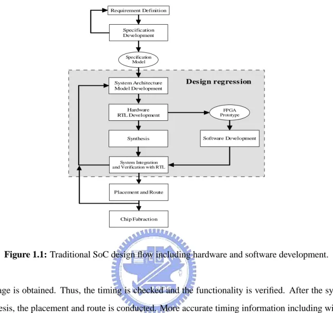
For ensuring the quality of the design, the SoC design flow involves various types of verification and validation. Figure 1.1 shows the traditional design flow, which can be roughly partitioned into two parts: (1) hardware development and (2) software development. As shown, the design flow starts with the requirements of the applications, from which the specifications of the design are defined. Further, according to the specifications, the tasks are partitioned and the system architecture is determined. After that, the hardware and software developments are initiated.
For the hardware development, the design go through modeling at different levels of ab-stractions, which include (1) algorithmic level, (2) RTL level, (3) gate level, and (4) physical level. Different issues are addressed at different levels of abstractions. At algorithmic level, the algorithms for the given task are studied. At this level of abstraction, we try to reduce the complexity by minimizing the number of operations and the size of memory. Further, given the algorithm, the RTL description maps the algorithm into hardware architecture. The data trans-fer from one register to another register at the cycle boundary is captured. Further down to gate level, the things happen in a cycle are extracted. The gate delay information within a pipeline
Chapter 1. Introduction Requirement Definition Specification Development Specification Model Hardware RTL Development FPGA Prototype Synthesis System Architecture Model Development Software Development System Integration and Verification with RTL
Placement and Route
Chip Fabraction
Des ign regress ion
Figure 1.1: Traditional SoC design flow including hardware and software development.
stage is obtained. Thus, the timing is checked and the functionality is verified. After the syn-thesis, the placement and route is conducted. More accurate timing information including wire and gate delays can be extracted. As illustrated, while the design starts from algorithmic level to physical level, more implementation details are discovered. The level of abstraction helps us to develop the hardware in a hierarchical and efficient manner.
For the software development, it is developed and verified after the system prototype is available. Normally, the system prototype is made of FPGA and board level components which may include CPU, memory, bus, I/O interface and so on. The FPGA helps to verify the hardware design while the other components emulate the target design. For verification, the interaction between software and hardware as well as timing information are tested. Generally, the software is verified and developed after the RTL descriptions of the hardware are available. After both hardware and software are developed, the system integration and verification are done by using either RTL or emulation board.
The traditional design flow poses some problems for the SoC design in which the system in-cludes more functionality and has higher complexity. Firstly, errors or misunderstanding could
easily occur between software and hardware because of independent development. Secondly, since system integration is started after software and hardware are available, any errors found in this stage could incur time-consuming regression process, which makes time to market become another issue. Thirdly, the complexity of the system could reach to a point that system level RTL simulation become inefficiency and meaningless. Although using FPGA for emulation could improve the efficiency, the emulation environment may not be exactly the same as the target design. Thus, the verification may not be done thoroughly. In summary, the traditional design flow cannot assure the reliability and quality of the design. It has difficulty to assure the first-time design success. Apparently, we need a new design methodology that improves the design quality and verification efficiency as well as reduces the time to market.
Recently, a modeling technique called transaction level modeling (TLM)[1][2][5][6] is pro-posed to address the problems of SoC design. It introduces an additional level of abstraction between system specification and RTL description. The purpose of TLM is to create a system architecture model that address issues at system level while maintaining necessary modeling accuracy. From the system perspective, the implementation details for each component are not the focuses in the early development phase. Instead, we do care about the system parameters such as the partition of tasks, the functionality of each component, the topology that connects different components, the communication protocol between components, and so on. The TLM is to hide unnecessary implementation details within a component and establish a system archi-tecture model that describes the system behavior. Due to the absence of implementation details, the TLM can simulate at a speed which is much faster than traditional RTL model. Also, it can exactly model the target platform. With faster simulation speed, it further helps on the explo-ration of design spaces and the reduction of the period for design regression. In addition, the TLM model serves as the unified platform for detailed software and hardware development. By using the TLM, the system verification and integration is started in the very beginning of the design flow, which significantly improves the chances for first-time silicon success. In terms of these advantages, the TLM nowadays attracts more attentions in the SoC design.
Chapter 1. Introduction
AR M 9 CPU
32-bits AHB Control Bus
128-bits AHB Control Bus
HDMI Interface Video
Pipe-CABAC,IQ/IDCT,DF,IIP,DeBlock,DeInterlacer
EMI
SD RAM0 SDR AM1 SD R AM2 SD R AM3
Hardware Input Interface
Bit-s tream FIFO
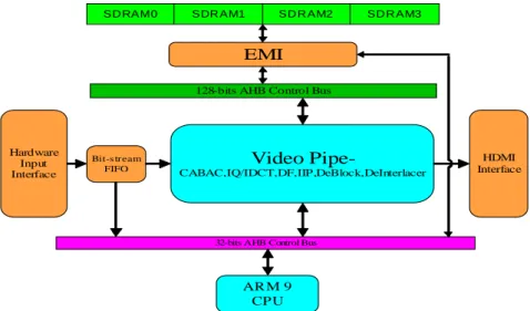
Figure 1.2: Overview of the system architecture.
1.1.3
System Level Modeling – H.264 Decoder
In this thesis, we propose a hardware architecture for the H.264 decoder that conforms to High profile at Level 4 (HP@L4). Moreover, we verify the system architecture using TLM. Fig. 1.2 depicts our system architecture, which mainly consists of the following components:
1. ARM 9 CPU.
2. 32-bit AHB control bus. 3. 128-bit AHB data bus.
4. Dedicated hardware vide pipe. 5. External memory interface (EMI). 6. Hardware input interface.
7. HDMI interface.
In our architecture, the bitstream is input from the hardware input interface and the decoded video is output through the HDMI interface. For the decoding, the ARM 9 CPU interprets the sequence parameter set, picture parameter set, and slice header. Then, it programs the hardware video pipe, which decodes the syntax elements under the slice data layer, via the 32-bit control bus. Particularly, during the decoding, the decoded frames/fields and the associated motion vectors are stored in the external DRAM. Thus, a dedicated 128-bit data bus is allocated for those modules which need intensive access to the DRAM.
For the decoding of slice data layer, the hardware video pipe contains the modules CABAC, IQ/IDCT, Data Fetch, Inter and Intra predictor, De-blocking, and De-interlacer. The CABAC operates at macroblock level while the other modules conduct computation at logical 8x8 block level, where each logical 8x8 block includes one 8x8 luma block and two 4x4 chroma blocks. In addition, since the data fetch, de-blocking, and de-interlacer modules shares the DRAM and the data bus, a bus arbitration policy is proposed to schedule the DRAM access. The details will be presented in Chapter 3.
To verify the system architecture, we use the techniques of TLM. In particular, the CABAC, IQ/IDCT, and de-blocking are done in pure C++ while the data fetch, inter and intra predic-tions, as well as de-interlacer are modeled with approximate-timed TLM. In addition, the ex-ternal memory interface and the DRAM are modeled at register-transfer-level (RTL); that is, those modules are described in Verilog. Thorough the simulation, we show the advantages and necessity of TLM. Also, we demonstrate how such a TLM model can be progressively refined.
1.1.4
Module Design – Inter and Intra Predictions
In addition to the system level modeling, we also propose a unified systolic-based architec-ture for the inter and intra predictions in H.264 decoder. In H.264/AVC [7], the inter and intra predictions are used to improve coding efficiency by using temporal and spatial redundancy. Comparing with the existing standards H.261/2/3 and MPEG-1/2/4 [8], these prediction tech-niques save up to 50% bit rates while providing similar perceptual quality.
However, the coding gain is at the cost of additional computations. In intra prediction, the mode-adaptive predictor is generated by a 1-D filtering, which is conducted along with the boundary pixels of a block. Similarly, the half-/quarter-pel predictor in the inter prediction is produced through a separable 2-D filtering with the motion compensated blocks of variable size. Both predictions require intensive filtering operations which poses challenges to real-time applications. Moreover, the adaptive and irregular filtering makes hardware implementation more difficult.
For the inter and intra predictions, most of the prior works implement the FIR filter based on the traditional adder-tree structure [9][10][11][12][13][14][15], where filtering is implemented by a number of adders and shifters. In such a straightforward implementation, common terms
Chapter 1. Introduction
between consecutive filtering operations are not reused. Moreover, multiple input samples are simultaneously latched for one filtered output causing higher input bandwidth.
In addition to less efficient FIR design, the inter and intra predictions are generally im-plemented by two separated modules due to the difference in their operations. However, in decoder, the prediction mode of each macroblock is known in advanced. Thus, using separated data paths for inter and intra predictions causes poor hardware utilization.
This thesis presents a unified systolic-based architecture for inter and intra predictions for H.264/AVC decoder. To increase hardware utilization and minimize cost, we combine inter and intra predictions by a re-programmable FIR filter, which is further implemented using systolic-based array. For intra prediction, the boundary pixels are reshuffled before feeding into the systolic-based array. For inter prediction, the 2-D interpolation is conducted through separa-ble 1-D filtering. As compared with the state-of-the-art approaches, our architecture provides higher performance while maintaining relatively lower cost and input bandwidth. Specifically, up to 4x throughput improvement has been achieved. Moreover, the input bandwidth is signifi-cantly reduced. Further, combining inter and intra predictions saves the cost by 22∼88%.
1.2
Organization and Contributions
In this thesis, we present a high level modeling technique, transaction level modeling (TLM), for the SoC design. Moreover, we use H.264 video decoder as an example and use TLM to verify the proposed system architecture. In addition, we also propose a unified systolic-based architecture for intra and inter predictions in H.264 decoder. As compared with the state-of-the-art designs, our design has higher throughput, but lower cost and power. For more details of each part, the rest of this thesis is organized as follows:
Chapter 2 introduces the concept of TLM and shows its benefits in designing SoC. Firstly, the bottleneck of traditional SoC design flow is presented. Then, we introduce the concept of TLM and illustrate how the TLM can be realized by using SystemC.
Chapter 3 describes the system architecture of our H.264 decoder and addresses the design issues at system level. Specifically, the design of the hardware video pipe, the system schedul-ing, the buffer allocation, and the bus arbitration policy are described. In addition, an optimal
solution for the bus arbitration policy is proposed based on the assumption that the input and output rates are of Poisson distribution. Lastly, the software architecture for the TLM is dis-cussed.
Chapter 4 shows the proposed systolic-based architecture for the intra and inter predictions. We show that combining inter and intra predictions by systolic-based architecture can signifi-cantly reduce the cost while the performance is also improved.
CHAPTER 2
Transaction Level Modeling
2.1
Introduction
As described in the previous chapter, the traditional design methodology can not satisfy the need for the design of complex system. The reason is that many unnecessary implementation details are captured for the system-level modeling. Thus, the simulation speed could be so slow that the verification at system level may not be done thoroughly.
Recently, a modeling technique called transaction level modeling (TLM) is proposed to ad-dress the system-level modeling. The idea is to introduce another level of abstraction between the system specification and its RTL implementation so that unnecessary implementation details can be hid from the system-level modeling. As far as the system is concerned, the implemen-tation details for each component are not the focuses in the early development phase. Instead, the system parameters, such as the partition of the tasks, the functionality of each component, the topology that connects different components, the communication protocol between compo-nents, the memory hierarchy, and so on, are of more interest.
sp ec ificatio n m odel
PE-ass em bly model
Bus -arb itration mod el
Time-acc urate c om mun icatio n mod el Cycle-accu rate com putatio n m od el
Imp lem en tation mod el
More Accurate Computation C om m uni ca ti on More Accurate Un-Timed Un-Timed Approxiate -Timed Approxiate -Timed Cycle-Timed Cycle -Timed SM TLM TLM TLM TLM RTL (1) (2) (3) (4) (1) (2) (3) (4) (a) (b)
Figure 2.1: System models at different levels of abstraction [1].
This chapter presents four types of TLM including (1) the PE-assembly model, (2) the bus-arbitration model, (3) the cycle-accurate computation model, and (4) the timing-accurate communication model. In addition, we show the benefits of introducing TLM in the SoC design flow. Lastly, we illustrate how TLM can be realized by using SystemC.
2.2
Definitions of Transaction Level Modeling
Figure 2.1 (a) shows the system models at different levels of abstraction. According to the mod-eling accuracy in computation and communication, each model represents an operating point in Figure 2.1 (b), where the bottom-left corner stands for the specification of the system while the top-right corner denotes the detailed implementation at register-transfer level. Particularly, only the four modules, PE-assembly model, bus-arbitration model, time-accurate communication model, and cycle-accurate computation model, are considered as the TLM. In the following, we will describe each model in detail.
2.2.1
Specification Model
Specification model describes the system functionality without any implementation details. Generally, the specification model is described in high level languages such as C/C++, Java
Chapter 2. Transaction Level Modeling v1 = a*a; B1 v2 = v1+b*b; B2 v3 = v1-b*b; B3 v4 = v2+v3; c=sequ(v4); B4 v1 v2 v3 B2B3
Figure 2.2: Example of the specification mode [1].
and so on. Such a model normally has no concept of timing, system architecture, and hardware implementation. Figure 2.2 illustrates an example of the specification model, in which the build-ing blocks B1, B2, B3, and B4 define the operation of the system. In addition, the variables v1, v2, and v3 represent the data transfer among different processes. As shown, the processes are executed sequentially and the data transfer among processes is done by transferring the address of the variables.
2.2.2
Implementation Model
Different from the specification model, the other extreme case is the implementation model, which describes the system with detailed implementation and is usually done with the hardware description languages such as Verilog, VHDL and so on. Normally, at this level of abstraction, the data transfer is at register level and the timing is of cycle accurate. Figure 2.3 illustrates an example of the implementation model, in which the PE1 and PE2 are the tasks executed on micro-processors while the PE3 and PE4 represent the tasks done by customized hardware modeled at register-transfer level (RTL). As you can see, the connections between all modules are pin-accurate. Moreover, the task is executed in a cycle-by-cycle manner.
PE3 S0 S1 S2 S3 PE4 S0 S1 S2 S3 PE1 P E2 Interconnect Network MOV r1,10 MUL r1,r1,r1 .... .... MLA r1,r2,r2,r1 ....
Figure 2.3: Example of the implementation model [1].
2.2.3
Transaction Level Model
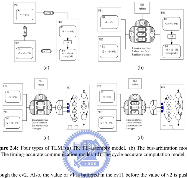
TLM provides more flexibility on selecting the level of abstraction for modeling. Generally, TLM can be classified into four types: (1) the PE-assembly model, (2) the bus-abstraction model, (3) the timing-accurate communication model, and (4) the cycle-accurate computation model. Each model has its own property, characteristic, and design purpose.
2.2.3.1 PE-Assembly Model
The PE-assembly model is to verify the correctness of the functionality and the data flow. In the PE-assembly model, the system is made up with multiple processing elements connected by channels. Different PEs executes concurrently and the data transfer among PEs is done through the channels, which are generally modeled by first-in-first-out (FIFO) buffer.
As compared to the specification model, the PE-assembly model has a rough view of system architecture. The sequential operations are now replaced with concurrent computations. In addition, the data transfer is modeled by FIFO, which is more similar to actual implementation. Particularly, the channel at this level of abstraction does not use any bus protocol and arbitration scheme. It is simply responsible for data transfer and synchronization. An example is shown in Figure 2.4 (a), where the PE3 needs both the intermediate variables v1 and v2 for computation. Note that the value of v1 is transmitted through the channel cv11 while the value of v2 is passed
Chapter 2. Transaction Level Modeling PE3 PE2 v1 = a*a; B1 v2 = v1+b*b; B2 v3 = v1-b*b; B3 v4 = v2+v3; c=sequ(v4); B4 v3 PE1 cv11 cv 1 2 cv2 PE3 PE2 v1 = a*a; B1 v2 = v1+b*b; B2 v3 = v1-b*b; B3 v4 = v2+v3; c=sequ(v4); B4 v3 PE1 cv11 cv12 cv2 PE4 Arbite r 1 2 3 1:master interface 2:slave interface 3:arbiter inte rface
(a) (b) PE3 PE2 v1 = a*a; B1 v2 = v1+b*b; B2 PE1 cv11 cv12 cv2 PE4 Arbiter 1 2 3 1:master interface 2:slave interface 3:arbiter interface 4:wrapper 4 S0 S1 S2 S3 PE3 PE2 v1 = a*a; B1 v2 = v1+b*b; B2 PE1 cv11 cv12 cv2 PE4 Arbiter 1 2 3 1:master interface 2:slave interface 3:arbiter interface 4:wrapper 4 S0 S1 S2 S3 (c) (d)
Figure 2.4: Four types of TLM. (a) The PE-assembly model. (b) The bus-arbitration model. (c) The timing-accurate communication model. (d) The cycle-accurate computation model. [1]
through the cv2. Also, the value of v1 is buffered in the cv11 before the value of v2 is pushed into the cv2. In this example, the PE3 can only start the computation when both v1 and v2 are buffered in the channel. As a result, the channels not only transfer the data but also synchronize the computations among different PEs.
2.2.3.2 Bus-Arbitration Model
The bus-arbitration model is to further refine the communication part of the PE-assembly model. Compared with the PE-assembly model, the bus-arbitration model includes more details in com-munication part. In some platform-based designs, the data transfer among different modules may not be through hard-wired connections. Instead, a centralized bus could be used to keep flexibility. An example is shown in Figure 2.4 (b), where the data transfer among PE1, PE2 and PE3 is done through a centralized bus. From the system perspective, the protocol of the bus and its arbitration scheme are critical to the system performance. Thus, the bus-arbitration model can help to verify the design of the communication part.
2.2.3.3 Timing-Accurate Communication Model
The timing-accurate communication model (as shown in Figure 2.4 (c)) is a refined version of the bus-arbitration model. Compared with the bus arbitration model, the timing-accurate communication model has more details in communication part. Precisely, the bus-arbitration model only cares about whether the data transfer is correct in a specific method while the timing-accurate communication model also considers the timing and signal transition for every data transaction.
2.2.3.4 Cycle-Accurate Computation Model
The cycle-accurate model is also a refined version of the bus-arbitration model. Compared with the timing-accurate communication model, the cycle-accurate computation model refines the computation part instead of the communication part. However, depending on the requirement, not all of the modules must be refined to cycle-accurate. An example is shown in Figure 2.4 (d), where only PE3 is refined in cycle-accurate while both PE1 and PE2 are remained the same. Such flexibility allows us to provide trade-off between simulation speed and modeling accuracy. Note that wrappers could be required to interface the modules modeled at different levels of abstraction.
2.2.3.5 Comparison
Table 2.1 summaries the characteristics of different system models. As shown, different models capture different degrees of accuracy in computation and communication. The specification model and the implementation model represent the two extreme cases, where the system model specifies the functionality of the system while the implementation model defines its implemen-tation at register-transfer level. The models in between are the four types of TLM, which offers the flexibility on selecting the simulation accuracy and speed.
2.3
Design Flow with Transaction Level Modeling
As described in Section 1.1.2, traditional design flow can not ensure the quality of the design when the system complexity increases dramatically. This section presents a new SoC design
Chapter 2. Transaction Level Modeling
Table 2.1: Characteristics of different abstraction models.
Models Communication Computation Communication PE Interface Implementation
Time Time Scheme Detail
Specification Model no no variable (no PE)
-PE-Assembly Model no approximate message-passing abstract PE allocation,
channel process PE mapping
Bus-Arbitration Model approximate approximate abstract bus abstract bus topology,
channel bus arbitration
Timing-Accurate time/cycle approximate detailed bus abstract detailed bus
Communication Model accurate channel protocol
Cycle-Accurate approximate cycle accurate abstract bus pin accurate RTL/ISS PEs
Computation Model channel detailed bus protocol
Implementation model cycle accurate cycle accurate wire pin accurate or RTL/ISS PEs
Requirement Definition
Specification Development
Specification Model
System Architecture and TLM Development TLM RTL HW Refinement SW Design and Development HW Verification Environment Development
Figure 2.5: Design flow with transaction level modeling [2].
flow with TLM as the common platform for concurrent software and hardware development. The new design flow mainly comprises two parts, which are (1) the new system-to-RTL exten-sion and (2) the traditional RTL-to-layout flow. The first part is different from that used in the past while the second part is remained the same.
Figure 2.5 depicts the new system-to-RTL extension. As shown, after the specification is defined, the system architecture is developed and verified by using TLM. Upon the complete-ness of the TLM model, it is used as an unique reference to both software and hardware teams.
For the software team, the embedded software is developed and verified based on the TLM model. For the hardware team, the TLM serves as the golden model for the detailed implemen-tation. Along with the development of software and hardware, the TLM model can be annotated with more accurate timing information. Consequentially, not only the functionality but also the timing can be jointly verified. Different from the traditional design flow, the new design flow performs system integration and verification in the very beginning, which is the key for ensur-ing the quality of the design. The followensur-ing summarizes the functionality of TLM in the SoC design flow:
1. Verification model for design space exploration. 2. Platform for early software development.
3. Specification and golden model for hardware development.
Nowadays, EDA tools are still not capable of automatically converting TLM to detailed hardware implementation. The hardware refinement is still done through a traditional paper specification and RTL coding. TLM appears to be an extra workload and unnecessary task. However, it still brings many benefits that significantly reduces the time to market:
1. System integration at the early stages so that the potential problems can be found and solved earlier.
2. Faster simulation speed while maintaining the accuracy of simulation. 3. Concurrent software and hardware development.
4. Platform for software/hardware co-design and co-verification.
5. Incremental hardware refinement and implementation details by means of hybrid abstrac-tion level modeling.
To show the benefits of TLM, Figure 2.6 illustrates the timeline for the development of SoC. The arrows highlight the differences between traditional design method and the one with TLM. The time scale in the figure depends on the project size, system complexity, and the makeup of the system component. Although writing a TLM model lengthens the architectural design phase, it enables earlier software implementation and architecture verification. Therefore, the design flow with TLM can reduce the overall development cycles. Besides, TLM has abilities to provide earlier and more realistic hardware/software trade-off at a time when changes are easier. Thus, the overall system quality is improved.
Chapter 2. Transaction Level Modeling
Figure 2.6: Comparison of design schedule between the traditional design flow and the one with transaction level modeling [2].
2.4
Transaction Level Modeling with SystemC
The SoC systems typically contain application-specific hardware and software. Both the hard-ware and softhard-ware are developed with a very tight schedule. Moreover, the systems have very rigorous constraints on performance. Therefore, the functional verification must be done thor-oughly so as to avoid expensive and sometimes catastrophic failures. Obviously, traditional hardware design languages such as VHDL and Verilog are not suitable for modeling at system level due to the lack of capability for traversing through different levels of abstraction. For improving the productivity, a design language for system level modeling is required.
2.4.1
Features of SystemC
SystemC, which is a class library built on top of the well established C++ language, is one of the candidates for TLM. It accepts original C/C++ syntax and additionally introduces a simu-lator that incorporates the concept of concurrent execution. The primary goal of SystemC is to enable system level modeling that includes both software modules, hardware modules and the combination of the two. With C++ syntax, it is easier to describe the behavior of a module in the very beginning from there the implementation detail can be developed later. Moreover, the simulator that includes the timing information allows us to model the concurrent execution of different modules. Furthermore, there are many tools that support co-simulation with SystemC
Figure 2.7: Separated computation and communication in SystemC
and RTL. As a result, one of the advantages of using SystemC for modeling is that one can develop models above RTL level and refine them to RTL level within the same environment.
To allow progressive refinement of system design, SystemC separates the computation and the communication. An example is shown in Figure 2.7. The computation part may be com-posed of different modules containing one or more processes while the communication part implemented as "channel" can also include many processes. The different computation mod-ules can exchange data through their ports connecting with channels by calling "interface func-tions". The only thing the computation part knows about the communication is how to transfer data between different modules by using interface functions of communication. With the sepa-ration of computation and communication, the designs for these two parts can be independently implemented and separately refined from algorithmic level to RTL level.
The capability of separated implementation for computation and communication is the key for transaction level modeling. Such modeling philosophy allows us to implement the computa-tion part and the communicacomputa-tion part at different levels of abstraccomputa-tions. As described in Seccomputa-tion 2.2, TLM may have different levels of timing resolution for computation and communication. In the very beginning for developing TLM, the computation and communication parts may have no concept about timing. The only thing one can verify at this stage is the correctness of func-tionality and data flow, which is one of the purposes for system level verification. After detailed micro-architecture is completed, one can refine the computation or the communication part to have approximated timing or cycle-accurate timing. However, it should be noted that the more details that are captured by the TLM, the slower is the simulation speed. In a special case where both computation and communication parts are of cycle- and pin-accurate, the TLM will then become almost the same as RTL. With such implementation details, the simulation speed could
Chapter 2. Transaction Level Modeling
be too slow to thoroughly verify the design. Thus, how to provide trade-off between simulation speed and accuracy is critical to the completeness of system level verification.
2.4.2
Implementation Using SystemC
2.4.2.1 Modules and Processes
SystemC offers two types of methods for implementing the concurrent processes contained in a channel or a module: sc_method and sc_thread.
The sc_method is the most basic type of simulation process. It works like "always" block in Verilog language and can be triggered by clock, event, or any signals. Different from sc_method, sc_thread is only invoked once and will not suspend itself until the wait function is executed. The wait function is to suspend the execution of current process and hands over the control of execution to other processes. Depending on whether the TLM is timed or untimed, the events in wait function or the ones for triggering the sc_method can have timing informa-tion. The resolution of timing information can be arbitrarily determined according to the details that should be captured.
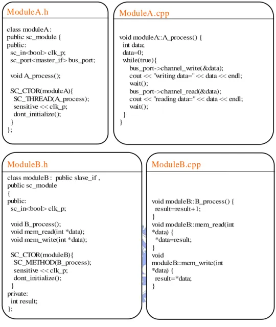
Figure 2.8 gives two examples of module implementation using the sc_thread and sc_method, respectively. As shown in the figure, a module may consist of ports, processes, as well as mem-ber functions and variables. The ports define the interface with which a module can commu-nicate with the others. The processes, on the other hand, specify the operations for a module. Further, the process can be encapsulated by sc_method or sc_thread so that it can be triggered by a set of pre-defined events. In moduleA, the process is triggered whenever the signal con-nected to the port of clk_p is changed. In this example, the moduleA firstly writes a value to moduleB through the channel and then suspend for 1 cycle. When the next event is raised, the moduleA further read a value form moduleB. On the other side of the channel, the moduleB responses to the request of moduleA by setting or returning the internal variable "result", which is increased by 1 whenever the process is triggered.
In SystemC, the simulation speed can be improved by reducing the number of context switch. In the example of moduleA, one must suspend the execution of a process contained in sc_thread so that the other processes can be granted for execution. Compared to traditional hardware description languages such as Verilog and VHDL, one can control the number of
con-ModuleA.h class moduleA : public sc_module { public: sc_in<bool> clk_p; sc_port<master_if> bus_port; void A_process(); SC_CTOR(moduleA){ SC_THREAD(A_process); sensitive << clk_p; dont_initialize(); } }; ModuleA.cpp void moduleA::A_process() { int data; data=0; while(true){ bus_port->channel_write(&data); cout << "writing data=" << data << endl; wait();
bus_port->channel_read(&data); cout << "reading data=" << data << endl; wait();
} }
ModuleB.h
class moduleB : public slave_if , public sc_module
{ public:
sc_in<bool> clk_p; void B_process(); void mem_read(int *data); void mem_write(int *data); SC_CTOR(moduleB){ SC_METHOD(B_process); sensitive << clk_p; dont_initialize(); } private: int result; }; ModuleB.cpp void moduleB::B_process() { result=result+1; } void moduleB::mem_read(int *data) { *data=result; } void moduleB::mem_write(int *data) { result=*data; }
Figure 2.8: Example of module implementation using sc_thread and sc_method.
text switch by properly determining when the execution should be switched to other processes. However, it should also be noted that the number of context switch could be reduced at the cost of losing model accuracy.
2.4.2.2 Channels and Interface Functions
For implementing the communication part, SystemC provides two types of channels: primitive channel and hierarchical channel.
The primitive channel is created for providing simple and fast communications. In the primitive channel, there is no hierarchy, ports, and methods. Besides, the primitive channel
Chapter 2. Transaction Level Modeling
uses the request-update mechanism to resolve the issue of concurrent read and write access; that is, when a value is passed to a module through the primitive channel, and the read and write operations are executed concurrently; the module will get the old value instead of the updated one. Such a request-update mechanism is helpful in modeling the hardware pipeline when using the primitive channel.
In contrast, the hierarchical channel is more flexible in a sense that it acts like a module. Actually, in SystemC, the difference of hierarchical channel and module only exists in users’ minds. There is no difference from the perspective of the simulator. In other words, what can be done in a module can also be done in a hierarchical channel. Normally, the hierarchical channel is used to implement complex communication protocols with timed or untimed constraints.
The processes of a channel are implemented in the interface functions, which are the key for separating the computation and the communication. For the process within a module, it com-municates with other modules by calling the interface functions bound to the ports. Normally, the definition of interface functions is kept untouched when the TLM is refined to different lev-els of abstraction. This feature ensures that the computation part and the communication part are independent because the changes in the computation part or the communication part will not affect the other.
Figure 2.9 shows the channel that connects moduleA and moduleB, as well as the cor-responding interface functions. In this example, when moduleA transmits data to moduleB through the channel, the data will be added with random noise. In this example, you can see that moduleA only knows how to use the interface functions for transmitting data. However, the details about how the data is transferred are hid by the interface functions. Thus, when the channel is refined, the way moduleA transmits data is still remained the same. This is the key idea of separating the computation and communication.
Figure 2.10 shows the overall architecture of the example. Compare with figure 2.7, this example keeps the rule of separating the computation part and the communication part. After the interface function is well defined, the modules and the channels can be implemented at the same time. It will also reduce the modeling time. In addition, you can exchange the modules or the channels as you want only using the same interface function. As a result, IP reusable is another benefit of separating the computation part and the communication part.
channel.h
class channel : public master_if, public sc_module { public: sc_port<slave_if> slave_port; SC_CTOR(channel){ }
void channel_read(int *data); void channel_write(int* data); }; channel.cpp void channel::channel_read(int *data) { slave_port->mem_read(data); *data=*data+rand()/10000; } void channel::channel_write(int *data) { *data=*data+rand()/10000; slave_port->mem_write(data); } master_if.h
class master_if : public virtual sc_interface {
public:
// master interface
virtual void channel_read(int *data)=0; virtual void channel_write(int *data)=0; };
slave_if.h
class slave_if :
public virtual sc_interface {
public:
// slave interface
virtual void mem_read(int *data)=0;
virtual void mem_write(int *data)=0;
}
Figure 2.9: Example of channel implementation and interface functions.
2.5
Summary
This chapter introduces a modeling technique, transaction-level modeling (TLM), for system-level modeling. Specifically, the TLM is to introduce another system-level of abstraction between the specification model and the detailed RTL model. By hiding unnecessary implementation details in the early development phase, the TLM enables the exploration of design spaces and the verification of system architecture. Moreover, it serves as a virtual platform for concurrent software and hardware development. With the TLM, the system integration and verification is initiated in the very beginning, which ensures the quality of the design and increases the chances of first-time silicon success.
Chapter 2. Transaction Level Modeling
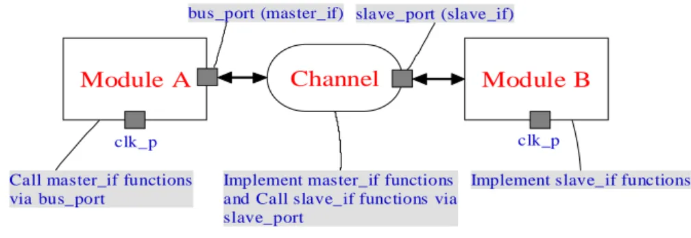
Module A Channel Module B
clk_p
bus_port (master_if)
clk_p slave_port (slave_if)
Call master_if functions via bus_port
Implement master_if functions and Call slave_if functions via slave_port
Implement slave_if functions
Figure 2.10: Top level connections for moduleA, moduleB, and the channel.
For the implementation of TLM, we present the SystemC library. In the SystemC, there are 3 major components, which are process, channel, and interface function. The processes define the operations of a component and can be triggered by a set of predefined events. In addition, the channel specifies the connections among different components and the interface function provides the means for a component to communicate with the others. Within a com-ponent, the processes can call the interface functions for data transaction without knowing the detailed implementation of the interface functions. Consequentially, by well defining the inter-face functions, the communication part and the computation part can be developed and refined independently.
Another feature of the SystemC library is that the simulator is not preemptive; that is, the designer must suspend the execution of a process so that the execution control can be switched to another process. Thus, the frequency of context switch can be controlled by the designer, which is a key to the trade-off between simulation speed and modeling accuracy. With so many features, the SystemC library now becomes one of the most popular tools for TLM.
Due to the benefits of the TLM, it will become an essential step in the SoC design flow. In the next chapter, we use H.264 video decoder as an example and demonstrate how TLM can be used to describe the system architecture.
Transaction Level Modeling of H.264
Decoder
3.1
Introduction
This chapter will describe the profile level of our H.264 decoder first. In most video coding standard, different profile level will support different coding tools such as transform8x8, sup-porting frame size, and MBAFF. As a result, the profile level definition is very important to the complexity and cost of the overall system architecture. Next, the system architecture will be in-troduced. The software and hardware partition, module partition and functionality, and system scheduling are included. Then, some important issues are discussed such as buffer allocation, control scheme, and so on. Finally, how we use SystemC to model our system of H2.64 decoder in transaction level is shown up.
Chapter 3. Transaction Level Modeling of H.264 Decoder
3.2
Design Specification
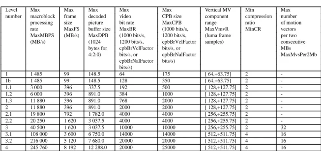
In H.264 standard, there are many different profile levels which contain different coding tools to improve the coding efficiency. Thus, different decoder design supporting for different profile will be different in performance and cost. This section presents a design specification of decoder conforming to high profile at level 4. Any bit-streams conforming to main/high profile with a level lower than or equal to 4 shall be decoded. Specifically, the decoder supports the decoding throughput up to 1920x1080i@60Hz. In the following, some properties of high profile and level limits are listed.
1. Only I, P, and B slice types may be present. 2. No data partition.
3. Arbitrary slice order is not allowed. 4. No slice group and no redundant picture. 5. chroma_format_idc in the range of 0 to 1.
6. bit_depth_luma_minus8/bit_depth_chroma_minus8 equal to 0 only. 7. qpprime_y_zero_transform_bypass_flag equal to 0 only.
8. Up to 16 reference frames. (32 reference fields).
9. Vertical motion vector range does not exceed MaxVmvR as in Table 3.1. 10. Horizontal motion vector range does not exceed the range of -2048 to 2047.75 11. Up to 32 MVs per MB.
12. Number of bits per macroblock is not greater than 3200.
Moreover, Table 3.1 and Table 3.2 show more constraints of different profiles. With sum-marizing these profile limits, we can start to design our micro-architecture of H.264 decoder to satisfy all functionalities while minimizing the cost.
3.3
System Architecture
Figure 3.1 shows the overall architecture of this system, which is developed based on the ARM platform. For the chip I/O, the compressed bit-stream is input via a hardware interface, which communicates with the host by a bridge, and the decoded frames are output to the monitor via HDMI interface. The reference pictures, decoded pictures, and MVs for each reference
Table 3.1: Level Limits I
Level Max Max Max Max Max Vertical MV Min Max number macroblock frame decoded video CPB size component compression number
processing size picture bit rate MaxCPB range ratio of motion rate MaxFS buffer size MaxBR (1000 bits/s, MaxVmvR MinCR vectors MaxMBPS (MB/s) MaxDPB (1000 bits/s, 1200 bits/s, (luma frame per two (MB/s) (1024 1200 bits/s, cpbBrVclFactor samples) consecutive
bytes for cpbBrVclFactor bits/s, or MBs
4:2:0) bits/s, or cpbBrNalFactor MaxMvsPer2Mb cpbBrNalFactor bits/s) bits/s) 1 1 485 99 148.5 64 175 [ 64,+63.75] 2 -1b 1 485 99 148.5 128 350 [ 64,+63.75] 2 -1.1 3 000 396 337.5 192 500 [ 128,+127.75] 2 -1.2 6 000 396 891.0 384 1000 [ 128,+127.75] 2 -1.3 11 880 396 891.0 768 2000 [ 128,+127.75] 2 -2 11 880 396 891.0 2000 2000 [ 128,+127.75] 2 -2.1 19 800 792 1 782.0 4000 4000 [ 256,+255.75] 2 -2.2 20 250 1 620 3 037.5 4000 4000 [ 256,+255.75] 2 -3 40 500 1 620 3 037.5 10000 10000 [ 256,+255.75] 2 32 3.1 108 000 3 600 6 750.0 14000 14000 [ 512,+511.75] 4 16 3.2 216 000 5 120 7 680.0 20000 20000 [ 512,+511.75] 4 16 4 245 760 8 192 12 288.0 20000 25000 [ 512,+511.75] 4 16
Table 3.2: Level Limits II
Level SliceRate MinLumaBiPredSize direct_8x8_inference_flag frame_mbs_only_flag
1 - - - 1 1b - - - 1 1.1 - - - 1 1.2 - - - 1 1.3 - - - 1 2 - - - 1 2.1 - - - -2.2 - - - -3 22 - 1 -3.1 60 8x8 1 -3.2 60 8x8 1 -4 60 8x8 1
-picture are stored in the external RAM. All the data access to external RAM will go through the memory interface.
Inside the chip, there is an embedded CPU and two AHB buses, which are control bus and data bus. The control bus is used by CPU for data flow control and the data bus is used by DF, De-blocking and De-interlacer for data transfer between these modules and external RAM. In addition to the AHB buses, there are backdoor-to-backdoor connections between modules. The modules connected by backdoor channel make up a video pipe, where its input comes from bit-stream FIFO and its output is drive to the HDMI interface. Particularly, the data between modules are exchanged on block by block basis with block size being 8x8 except for CABAC.
Chapter 3. Transaction Level Modeling of H.264 Decoder
32-bit AHB Control Bus
External Memory Interface S
SDRAM 0
CABAC CAVLC
S
128-bit AHB Data Bus
Bit-stream FIFO ARM 9 CPU M Instruction Memory Data Memory IQ/IDCT S MB Texture Buffer MB Motion Buffer Data Fetch S Intra/Inter Prediction S Subblock Reconstruct Buffer DeBlocking S,M IIP FIFO DB FIFO DeInterlacer S,M DI FIFO
SDRAM 1 SDRAM 2 SDRAM 3
Harddware Input Interface
M,M Sync FIFO HDMI Interface S u b b l o c k P r o c e s s i n g U n i t NAL Parsing
Figure 3.1: System architecture diagram[3][4].
In this system, after CABAC decodes the data above slice header, it will send an interrupt to CPU and then CPU will fetch the information in the headers of sequence, picture, and slice from CPU through control bus. According to the information in sequence, picture, and slice headers, CPU can configure the modules in the video pipe through the control bus for various decoding modes. Each module can also be independently tested by CPU. The following briefly describes our video pipe and system schedule.
3.3.1
Video Pipe
In our H.264 decoder, our video pipe contains seven modules which are CABAC, IQ/IDCT, Data Fetch(DF), Intra-Inter prediction(IIP), De-Blocking, and De-Interlacer. CABAC is the first module in video pipe and the functionality of CABAC is decoding all bit-stream syntax. Because our decoder processes luma and chroma components in parallel and CABAC can not decode chroma components until all luma coefficients have decoded in one macroblock, it is more efficient to make CABAC operate in macroblock level. Therefore, for saving the buffer size, all other modules operate in eight-by-eight block.
1 3 5 624 2 1 5 384 6 9 7 10 3 4 152 6 84 1 2 5 3 6 9 7 10 (a) (b) (c) (d)
Figure 3.2: Deblocking process order in eight by eight block
quantization and inverse discrete cosine transform of the residuals while the DF module is re-sponsible for motion prediction and fetching reference block for Inter block and intra prediction type decoding for Intra block. Following after the DF is IIP which produces the value of predic-tion block for Intra and inter predicpredic-tion and adds the results with the residuals from IQ/IDCT. Because we let IQ/IDCT start earlier one eight by eight block than IIP, it can make sure that IIP always has the corresponding residuals.
After that, de-blocking is performed for reducing the blocking effect. Because IQ/IDCT starts earlier than IIP by one eight by eight block cycle for keeping the correct data order, we use three eight by eight block buffers between IQ/IDCT, IIP, and De-Block. For example, when IQ/IDCT is writing the third buffer and IIP is writing the second buffer, De-Block is reading the first block buffer. In addition, because deblocking has specific process order in macroblock level but our process unit is eight by eight block, we must change the process order shown in Figure 3.2 and still follow the rule in specification. In Figure 3.2, (a), (b), (c), and (d) present the eight by eight block order in zig-zag scan of one macroblock and the number means the process order in one block..
The last module is De-Interlacer which will work only when the source sequence is field. The functionality of De-Interlacer is to translate a field picture to a frame picture. Because the algorithm of De-Interlacer will use the previous, current, and next one field in display order, it will also need amount of bus bandwidth. Besides, the fields for De-Interlacer and for reference may be different. As a result, it will also increase the size of external memory.
3.3.2
System Schedule
Without a system schedule to control data flow in video pipe, it is possible that the functionality of whole system is wrong even if every module is well verified. This section describes briefly
Chapter 3. Transaction Level Modeling of H.264 Decoder
our system schedule shown in Table 3.3. In the beginning of decoding, we need a initial period to decoding bitstream above slice header by CABAC and to set the control registers of every hardware modules by ARM CPU. After that, all hardware modules start to decode one by one. When CABAC starts to decode the second macroblock in current slice, the first macroblock is fed into the following modules in eight by eight block unit. As a result, IQ/IDCT and DF, IIP, and DeBlock process the different eight by eight block.
During the slice changes, the CABAC will detect the NAL unit first and start to decode the slice header. When CABAC is decoding the slice, the hardware may stall depending on the time the NAL unit is detected, slice header decoding speed of CABAC, and block decoding speed of hardware modules. Table 3.3 shows the condition that hardware modules will stall. In addition, when the picture changes, there is same condition as slice.
Looking into the hardware pipe, every module has different process time. As a result, when a module finish current block, it does not mean that the module can process next block right now because the input data may be not ready and it may over write the data which next stage is using. In our decoder design, if one module is finished, it will not start again until all hardware modules are finished. Thus, for supporting real-time decoding, all modules must make sure that they can finish their job in time.
3.4
Bus Arbitration Policy
In our architecture, the data bus and the external memory are shared by the data fetch, deblock-ing, and deinterlacer modules. The data fetch module reads the reference block from the exter-nal memory for motion compensation. On the other hand, the deblocking module writes back the reconstructed block. In addition, the deinterlacer further reads the decoded fields buffered in the external memory for display. Due to limited resources, different modules must be scheduled for the access of bus and external memory.
To prevent the hardware from stall, each module needs to allocate a local buffer, which acts as a first-in-first-out (FIFO) buffer, to store the input/output data before it is granted for access-ing the bus and memory. Particularly, the size of the local buffer is determined by how frequent a module is granted for accessing the bus. Moreover, it also depends on the consumption or
Table 3.3: System Schedule
Field(t1) Field(t2)
8x8 CABAC IQ/IDCT IIP DeBlock DeInterlacer
Cycles and DF
Detect NAL Initial of sequence Dec SPS
Set SPS_CR
Detect NAL Initial of fist picture Dec PPS_0
Set PPS_CR[0]
Detect NAL Initial of first slice Dec SH_0 Set SH_CR[0] 0 P0S0B0 B0 1 P0S0B1 P0S0B0 B1 2 P0S0B2 P0S0B1 P0S0B0 B2 3 P0S0B3 P0S0B2 P0S0B1 P0S0B0 B3 . . P0S0B3 P0S0B2 P0S0B1 . . . . P0S0B3 P0S0B2 . . . . . P0S0B3 . 479 P0S0B479 . . . B479 480 Bubble P0S0B479 . . Bubble 481 P0S1B0 Bubble P0S0B479 . B480 482 P0S1B1 P0S1B0 Bubble P0S0B479 B481 483 P0S1B2 P0S1B1 P0S1B0 Bubble B482 484 P0S1B3 P0S1B2 P0S1B1 P0S1B0 B483 . . P0S1B3 P0S1B2 P0S1B1 . . . . P0S1B3 P0S1B2 . . . . . P0S1B3 . 959 P0S1B479 . . . B959 . . . . . . . . . . . . . . . .
. Detect NAL P0SNB479 Bubble
. Dec PPS_1
. Set PPS_CR[1]
. Detect NAL Bubble P0SNB479 Bubble
. Dec SH_1 . Set SH_CR[1] 0 P1S0B0 Bubble Bubble P0SNB479 B0 1 P1S0B1 P1S0B0 Bubble Bubble B1 2 P1S0B2 P1S0B1 P1S0B0 Bubble B2 . . P1S0B2 P1S0B1 P1S0B0 . . . . P1S0B2 P1S0B1 . . . . . P1S0B2 .
Chapter 3. Transaction Level Modeling of H.264 Decoder
λ
B u
Figure 3.3: Input and output configuration.
production rate of a module. With very different types of operations, different modules have different input and output rates. Thus, our goal is to design a bus arbitration policy according to these factors so that the total buffer size is minimized.
In the following, we present an optimal arbitration policy by assuming that the data arrival rate (input/output rate) has Poisson distribution, which is widely used to solve such a queuing problem and provides a good approximation to practical scenario. Then, from the optimal solutions, we show the guidelines for designing the bus arbitration policy and buffer allocation. After that, we present the bus arbitration policy and the buffer allocation scheme in our design.
3.4.1
Optimal Solution
3.4.2
Expected Buffer Size
The optimal bus arbitration policy is to minimize the sum of the expected buffer size. Before we go further to describe the bus arbitration policy, the following firstly formulizes the expected buffer size given the input and output rate. Figure 3.3 shows the configuration of the input and output rate. Particularly, we assume
1. The input rate (arrival rate) is λ, where λ has Poisson distribution.
2. The output rate is μ, where μ stands for the consumption rate of a module and is also characterized by Poisson distribution.
3. μ > λ.
Then, from the queuing theory, the expected buffer size E[B] can be derived as in Eq. (3.1).
E[B] = λ
Memory λ 2 μ 1 μ μ3 μN 1 B B2 B3 BN 1 P P2 P3 PN (a) λ 1 B 2 B N B 1 P 2 P N P 1 μ 2 μ N μ (b)
Figure 3.4: Input and output configuration with 3 PEs
3.4.2.1 Multiple Processing Elements with Consumption Model
To understand the cases with multiple processing elements that simultaneously read the memory through a centralized bus, the configuration in Figure 3.3 is further extended to have multiple processing elements. Figure 3.4 illustrates such a configuration, where we assume
1. There are N processing elements that share the bandwidth of a centralized bus, λ.
2. Each processing element retrieves the data stored in the memory through the centralized bus.
3. The processing element j has a consumption rate of μj, where j = 1 ∼ N and μT =
XN
j=1μj > λ.
The goal is to find the probability Pj, i.e, the bus arbitration policy, that minimizes the sum
of the expected buffer size E[BT otal] = E[
XN
j=1Bj] =
XN
j=1 Pjλ
μj−Pjλ and satisfies the two constraints:
1. μj > Pjλ.
2. XN
j=1Pj = 1, where 0≤ Pj ≤ 1.
The solution to the problem with the two constraints can be obtained by using the Lagrange multiplier. According to the Lagrange optimization theory, the problem above can be
![Figure 2.1: System models at different levels of abstraction [1].](https://thumb-ap.123doks.com/thumbv2/9libinfo/7634627.136041/24.892.170.769.110.430/figure-system-models-different-levels-of-abstraction.webp)
![Figure 2.5: Design flow with transaction level modeling [2].](https://thumb-ap.123doks.com/thumbv2/9libinfo/7634627.136041/29.892.116.817.157.382/figure-design-flow-transaction-level-modeling.webp)
![Figure 2.6: Comparison of design schedule between the traditional design flow and the one with transaction level modeling [2].](https://thumb-ap.123doks.com/thumbv2/9libinfo/7634627.136041/31.892.291.641.112.378/figure-comparison-design-schedule-traditional-design-transaction-modeling.webp)
![Figure 3.1: System architecture diagram[3][4].](https://thumb-ap.123doks.com/thumbv2/9libinfo/7634627.136041/41.892.135.801.112.486/figure-system-architecture-diagram.webp)
