This content has been downloaded from IOPscience. Please scroll down to see the full text.
Download details:
IP Address: 140.113.38.11
This content was downloaded on 25/12/2014 at 01:59
Please note that terms and conditions apply.
Homogeneous barrier modulation of TaOx/TiO2 bilayers for ultra-high endurance
three-dimensional storage-class memory
View the table of contents for this issue, or go to the journal homepage for more 2014 Nanotechnology 25 165202
(http://iopscience.iop.org/0957-4484/25/16/165202)
Chung-Wei Hsu
1, Yu-Fen Wang
1, Chia-Chen Wan
1, I-Ting Wang
1,
Chun-Tse Chou
1, Wei-Li Lai
1, Yao-Jen Lee
2and Tuo-Hung Hou
11Department of Electronics Engineering and Institute of Electronics, National Chiao Tung University, Hsinchu, Taiwan
2National Nano Device Laboratories, Hsinchu, Taiwan
E-mail:thhou@mail.nctu.edu.tw
Received 26 December 2013, revised 14 February 2014 Accepted for publication 26 February 2014
Published 28 March 2014
Abstract
Three-dimensional vertical resistive-switching random access memory (V-RRAM) is the most anticipated candidate for fulfilling the strict requirements of the disruptive storage-class memory technology, including low bit cost, fast access time, low-power nonvolatile storage, and excellent endurance. However, an essential self-selecting resistive-switching cell that satisfies these requirements has yet to be developed. In this study, we developed a TaOx/TiO2 double-layer V-RRAM containing numerous highly desired features, including: (1) a
self-rectifying ratio of up to 103with a sub-µA operating current, (2) little cycle-to-cycle and layer-to-layer variation, (3) a steep vertical sidewall profile for high-density integration, (4) forming-free and self-compliance characteristics for a simple peripheral circuit design, and (5) an extrapolated endurance of over 1015cycles at 100◦C. Furthermore, the switching and self-rectifying mechanisms were successfully modeled using oxygen ion migration and homogeneous barrier modulation. We also suggest the new possibility of monolithically integrating working and storage memory by exploiting a unique tradeoff between retention time and endurance.
Keywords: storage-class memory, resistive-switching random access memory, three-dimensional memory, current conduction mechanism, self rectification
S Online supplementary data available fromstacks.iop.org/Nano/25/165202/mmedia
(Some figures may appear in colour only in the online journal)
1. Introduction
Inefficient memory and storage hierarchy based on dynamic random access memory (DRAM) and hard disks has become a major challenge in designing large-scale, high-performance computer systems. Using the existing hierarchy, the projected exascale computing requires impractical energy consumption, space usage, and cost [1]. This inefficiency is largely attributed to the access time gap of five orders of magnitude between hard disks (>10 ms) and DRAM (<100 ns). Storage-class memory (SCM) has been proposed to narrow or even eliminate
the access time gap and greatly improve system performance [1,2]. The basic requirements for SCM include low cost per bit, fast read and write access time, low-power nonvolatile storage, and excellent write endurance. However, none of the existing or emerging memory technologies can fulfill all of the requirements for SCM simultaneously. Solid-state drives based on NAND flash nonvolatile memory (NVM) are considered an early version of SCM. Recent advances in three-dimensional (3D) vertical NAND (V-NAND) technology may eventually realize SCM at a bit cost comparable to that of hard disks [3,4]. However, slow access time and poor write endurance
Nanotechnology25 (2014) 165202 C-W Hsu et al
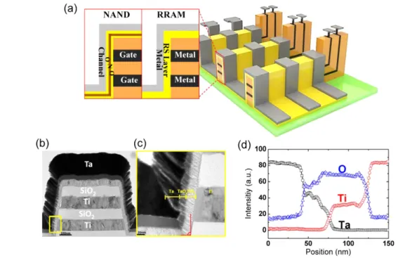
Figure 1. (a) Illustration of 3D V-NAND and V-RRAM arrays for realizing high-bit-density SCM. Unit cells for both 3D V-NAND and V-RRAM on the vertical sidewalls are shown for comparison. (b) Cross-sectional TEM image of the 3D double-layer V-RRAM, showing a steep sidewall profile. (c) Enlarged picture of the Ta/TaOx/TiO2/Ti MIIM unit cell as indicated in (b). The thicknesses of TiO2and TaOx
on the vertical sidewalls are 40 nm and 20 nm, respectively. (d) EDX elemental profiling of the MIIM cell.
may limit the full potential of NAND-based SCM. Phase-change memory (PCM) is considered an alternative SCM possessing a faster access time than NAND. However, the high programming current of PCM is the main concern for high-density integration [2]. Although a programming current as low as 1 µA was recently demonstrated by using car-bon nanotubes as nanoscale electrodes [5,6], a high-density integration scheme as competitive as 3D V-NAND has yet to be developed. Emerging resistive-switching random access memory (RRAM) [7–12] is another strong candidate for high-performance SCM. The latest RRAM array prototypes have demonstrated a fast access time, closer to that of DRAM [13], endurance of over 107 cycles [14], and a high integration density of 32 Gb by using the 24-nm technology [15]. Further-more, 3D vertical RRAM (V-RRAM) technology, analogous to the V-NAND counterpart, is being actively developed to fabricate high-density memory in an extremely cost-effective manner [16–18]. Figure 1 illustrates the representative cell structures of V-RRAM and V-NAND. Both V-RRAM and V-NAND use multiple thin-film deposition and minimal pho-tolithography and etching steps. Oxide/nitride/oxide (ONO) layers, used for local charge storage, and resistive-switching (RS) layers are deposited on the vertical sidewalls of V-NAND and V-RRAM, respectively. Requiring no serial Si transistors in the memory core of V-RRAM not only enables fast random access in a cross-point configuration, but also allows ultimate scalability beyond the conventional transistor scaling limits. In addition, the insufficient number of stored electrons (less than 100) is a known physical limit of NAND technology below 20 nm [19]. By contrast, RRAM has shown promising scalability beyond 10 nm [20].
Two critical challenges remain for V-RRAM in becom-ing a legitimate SCM candidate. First, self-selectbecom-ing or self-rectifying characteristics involving a highly nonlinear resistance are required in high-density cross-point V-RRAM to suppress the sneak current in read and write opera-tions [21–23]. Otherwise, the sneak current through the neighboring unselected cells would degrade readout signals, attenuate voltage propagation, and increase read/write power consumption [24–26]. The V-RRAM devices reported in the literature either lacked sufficient selectivity [16,17] or were incompatible with semiconductor fabrication owing to their use of noble metal electrodes such as Pt [18]. Furthermore, the physical mechanism and design principles used to realize the desired selectivity are not comprehensively understood. Sec-ond, although far superior to flash, a write endurance of RRAM that satisfies the demanding requirements for replacing DRAM as working memory (>1015 cycles) has yet to be achieved. Recently, a self-rectifying RRAM based on a TaOx/TiO2 bilayer structure has exhibited numerous highly desirable features for implementing high-density cross-point arrays [23]. In this paper, we report on a Ta/TaOx/TiO2/Ti V-RRAM which demonstrates a substantial self-rectifying ratio of 103 with a sub-µA operating current and extrapolated endurance of over 1015 cycles at 100 ◦C. The RS and self-rectifying mechanisms were successfully modeled using oxygen ion (O2−) migration in TaOx, corresponding homogeneous barrier modulation, and asymmetric tunnel barriers at the Ta/TaOx and TaOx/TiO2 interfaces. Furthermore, a tradeoff between retention time and endurance may enable the monolithic integration of DRAM-like and NVM-like SCM using identical V-RRAM technology.
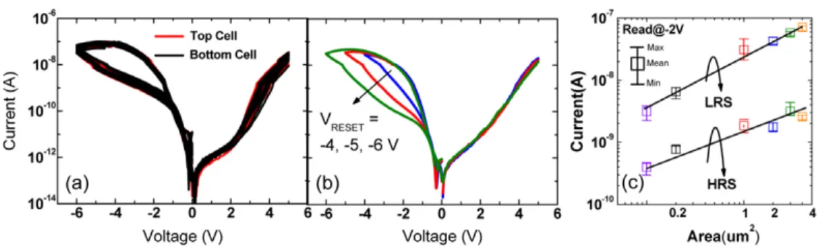
Figure 2. (a) Typical BRS I –V curves (30 cycles appended) of the MIIM V-RRAM, exhibiting little switching variation and no apparent difference between top-layer and bottom-layer cells. The effective device area at the vertical sidewall is 0.2 µm2. The device demonstrates a
sub-µA operating current and an RR of 103at ±2 V. (b) Multiple resistance states controlled using a gradual RESET process. (c) Devices
comprise varied sidewall lengths from 0.6 to 20µm and a fixed Ti thickness of 100 nm (effective areas of 0.12–4 µm2). Both the LRS and HRS currents are scaled according to the device area.
2. Experimental details
We fabricated a double-layer V-RRAM, similar to that shown in figure 1. Multiple Ti horizontal electrodes and SiO2 isolation layers were sequentially deposited onto 550-nm-thick SiO2 substrates. For the Ti electrodes, 100-nm-thick Ti was deposited using dc magnetron sputtering with a Ti (99.99%) target at a deposition rate of 1 nm s−1. For the SiO2isolation layers, 100-nm-thick SiO2was deposited using plasma-enhanced chemical vapor deposition (PECVD) at 320◦C and tetraethyl orthosilicate (TEOS) as a silicon source at a deposition rate of 1.7 nm s−1. Vertical pillar structures with a sidewall width of 0.5 µm were patterned using a lithography process, followed by etching multiple Ti and SiO2 layers, with the etchants HBr6 and CCl4, respectively, until the SiO2substrates were reached. To prepare the bilayer TaOx/TiO2, 60-nm-thick TiO2 and 40-nm-thick TaOx were sequentially deposited by means of reactive dc magnetron sputtering at room temperature using Ti (99.99%) and Ta (99.95%) targets, respectively, in an Ar and O2mixture. The Ar to O2gas flow ratio and the deposition rate for TiO2were 2:1 and 0.006 nm s−1, whereas those for TaOx were 20:3 and 0.04 nm s−1. Two additional lithography and dry etching steps were performed to open the contacts to the Ti horizontal electrodes for the top and bottom cells. Finally, the shape of the Ta vertical electrodes with a thickness of 250 nm and various sidewall lengths from 0.2 to 20 µm were deposited using dc magnetron sputtering with a Ta (99.95%) target at a deposition rate of 0.1 nm s−1, followed by a lift-off process completing the Ta/TaOx/TiO2/Ti metal–insulator–insulator– metal (MIIM) RRAM unit cell on the vertical sidewalls.
A transmission electron microscopy (TEM) image of the double-layer V-RRAM is shown in figure1(b). In contrast to the tapered sidewall with a Pt bottom electrode [18], using the fab-friendly Ti horizontal electrode formed a steep sidewall profile, which is critical in reducing the pitch size between vertical pillars in a high-density array with a large number of vertically stacked layers. Because of the nonconformal deposition of the sputtered films, the film appeared to be thinner on the vertical sidewall (20-nm TaOx and 40-nm TiO2) but thicker on the top of the pillar structure. An
enlarged TEM image of the TaOx/TiO2 bilayer is shown in figure1(c). The Ti and TiO2 films were highly crystalline, with an amorphous 20-nm-thick interfacial layer formed by oxidizing the Ti electrode during the reactive sputtering process. The crystallinity of the Ta and TaOx films was greatly enhanced at the sidewall, thereby forming columnar grains with the TiO2 underlayer. The elemental analysis by energy-dispersive x-ray spectroscopy (EDX) shown in figure 1(d) reveals a nearly stoichiometric TiO2 layer, an oxygen-deficient TiOx (x< 2) interfacial layer, and a TaOx layer with a gradient substoichiometric composition. The TaOx became more oxygen-deficient toward the Ta top electrode, suggesting a strong oxygen scavenging ability of Ta because of its low electronegativity. The results of a separate analysis using x-ray photoelectron spectroscopy (XPS) were consistent with the EDX results (figure S1, supporting information available atstacks.iop.org/Nano/25/165202/mmedia). 3. Results and discussion
Figure2(a) shows the typical bipolar resistive switching (BRS) characteristics of the MIIM V-RRAM with a sub-µA operating current. The effective device area at the vertical sidewall was 0.2 µm2. The device operation required neither electrical forming nor current compliance, which greatly reduces the complexity of the peripheral circuit design. We observed little switching variation and no apparent difference between the top-layer and bottom-layer cells. Excessive switching variability is known to be a major bottleneck of the typical filamentary RRAM because of the stochastic nature of the percolation-based SET process [27, 28]. A previous study reported that the variability became even more severe in a sub-µA filamentary RRAM because of the unavoidable random fluctuation of very few ions moving at SET/RESET in the filament constriction [29]. By contrast, the results of this study support the possibility of developing a low-power RRAM with minimal variability. A tenfold resistance change in a high resistance state (HRS) and a low resistance state (LRS) could be read only at a negative (forward) bias because the current–voltage (I –V ) curves completely overlapped at a positive (reverse) bias. A rectifying ratio (RR) of an LRS at
Nanotechnology25 (2014) 165202 C-W Hsu et al
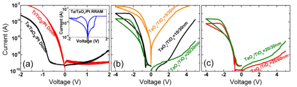
Figure 3. I–V curves of several shadow-mask planar devices with an area of 3 × 104µm2and various TaOxand TiO2thicknesses. All of
the film deposition conditions were identical to those used in the 3D V-RRAM devices. (a) Typical rectifying I –V curves of the
Ti/TiO2(60 nm)/Pt and Ta/TaOx(20 nm)/Pt MIM. No RS was observed before electrical forming. Inset shows the BRS I –V curves with
gradual RESET in the Ta/TaOx/Pt MIM after electrical forming. (b) Typical BRS I –V curves of the Ta/TaOx/TiO2/Ti MIIM with a fixed
TiO2thickness of 30 nm and various TaOxthicknesses from 5 to 20 nm. (c) Typical BRS I –V curves of the Ta/TaOx/TiO2/Ti MIIM with
a fixed TaOxthickness of 20 nm and TiO2thicknesses of 30 and 60 nm.
±2 V that exceeds three orders of magnitude may effectively suppress the sneak current in high-density 3D arrays. Although the rectifying LRS resembled that of typical one diode–one resistor (1D1R) cells, this self-rectifying BRS device provided a wider programming margin by using opposite polarities of SET and RESET voltages compared with the unipolar resistive switching (URS) of 1D1Rs.
Figure2(b) shows a gradual RESET process that enables multiple resistance states to be precisely controlled using an appropriate RESET voltage, ranging from −4 to −6 V, and a SET voltage of 5 V. The gradual RESET is a signature of increasing tunnel distance in the HRS, most often involving O2−migration in the RS layers [30]. Figure2(c) shows the BRS curves of V-RRAM with varied sidewall lengths from 0.6 to 20µm and a fixed Ti thickness of 100 nm. Both the LRS and HRS currents showed an apparent area dependence, thereby supporting a homogeneous transport mechanism that is substantially different from the filamentary conduction often observed in RRAM devices [31–34].
To elucidate the RS mechanism of the Ta/TaOx/TiO2/Ti device, we fabricated several planar devices with various com-binations of TaOx and TiO2thicknesses by using a short-loop shadow-mask process. Both the Ta/TiO2/Ti and Ta/TaOx/Ti devices with only a single dielectric layer were highly conduc-tive at both polarities without RS (figure S2, supporting infor-mation available atstacks.iop.org/Nano/25/165202/mmedia). Ti is known as an extremely active metal that easily reacts with deposited metal oxides [35]. Therefore, separate devices of Ti/TiO2/Pt and Ta/TaOx/Pt were fabricated using inert Pt bottom electrodes to investigate the roles of the Ti/TiO2 and Ta/TaOx interfaces in RS. As shown in figure 3(a), both devices exhibited rectifying I –V because of the asym-metric Schottky barriers at the Ti/TiO2 (Ta/TaOx) and TiO2/Pt (TaOx/Pt) interfaces. A higher forward current in the Ti/TiO2/Pt device indicates that the Ti/TiO2interface formed a more ohmic-like transparent barrier [33,35] compared with that of the Ta/TaOx interface [36]. After electrical forming occurred at a positive bias with a current compliance of 1 mA, only the Ta/TaOx/Pt device demonstrated reproducible BRS with gradual RESET characteristics, as shown in the inset
of figure3(a). In addition, figure 3(b) shows the BRS I –V of Ta/TaOx/TiO2/Ti devices with various TaOx thicknesses. Reducing the TaOx thickness increased both the forward and reverse currents. The increase in the reverse current was more dramatic and, thus, the RR was degraded when a thinner TaOx film was used. The resistance ratio between the HRS and LRS also reduced when a thinner TaOxfilm was used. By contrast, the effect of the TiO2thickness on device currents was secondary, as shown in figure3(c). However, a sufficient TiO2 thickness was necessary to achieve RS and self-rectifying. Otherwise, the device would behave like the Ta/TaOx/Ti structure, possibly because of the strong oxygen scavenging ability of Ti (figure S3, supporting information available at
stacks.iop.org/Nano/25/165202/mmedia).
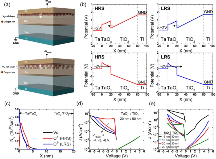
We proposed a plausible physical model, as shown in figure4(a), to explain the experimental findings. The TiO2/Ti interface is believed to be a transparent ohmic contact. There-fore, electron injection from the Ti electrode at a positive bias is limited mainly by the conduction band offset at the TaOx/TiO2 interface. In addition, electron injection from the Ta electrode at a negative bias is controlled by the Ta/TaOxinterface with a Schottky barrier height of 0.75 eV [36]. According to the gradient substoichiometric TaOx composition observed using EDX and XPS analysis, a large number of defects consisting of negative O2− and oxygen vacancies (VO) is expected to reside near the Ta/TaOx interface. O2− may easily migrate by applying a bipolar electric field while VO are treated as immobile shallow donor-like dopants. Varying charge distri-butions near the Ta/TaOx interface affect the tunnel width of the Schottky barrier at a negative bias, corresponding to multiple resistance states, but have little influence on the tunnel width of the TaOx/TiO2 barrier at a positive bias. Because of the homogeneous nature of current conduction, a one-dimensional (1D) numerical simulation of O2−migration and homogeneous barrier modulation was performed to verify the proposed physical model. The detailed simulation method is discussed in the supporting information (available atstacks. iop.org/Nano/25/165202/mmedia). Figures4(b) and (c) show the calculated band structures of the LRS and HRS at ±2 V and the corresponding VO and O2− concentration profiles,
Figure 4. (a) Schematic diagrams showing O2−migration in the VO-rich (oxygen-deficient) layer near the top Ta electrode during bipolar
SET and RESET operations. (b) Calculated band diagrams of the HRS and LRS in a Ta/TaOx(20 nm)/TiO2(60 nm)/Ti MIIM in ±2 V read
operations and (c) corresponding VOand O2−concentration profiles. Varying charge distributions near the Ta/TaOxinterface affect the
tunnel width of the Ta/TaOxSchottky barrier at −2 V but not the tunnel width of the TaOx/TiO2barrier at +2 V. (d) Calculated I –V curves
of the Ta/TaOx(20 nm)/TiO2(60 nm)/Ti MIIM, displaying multiple resistance levels. (e) Calculated I –V curves of several MIIM devices
with various TaOxand TiO2thicknesses, showing good qualitative agreement with the experiments (figures3(b) and (c)) using a single set
of parameters.
which confirm the presence of O2−migration, Schottky barrier modulation at the Ta/TaOx interface, and asymmetric tunnel barriers at positive and negative polarities. Note that the homogeneous barrier modulation involving a large number of interface defects in the entire device area overcomes the limitation of the stochastic percolation statistics and random fluctuation of very few ions in the filament constriction and is, thus, the key to realize deterministic BRS. Maintaining a gradient TaOx composition (i.e., more oxygen-deficient near the Ta/TaOx interface but less so near the TaOx/TiO2 inter-face) is critical for achieving the desired resistance ratio and the asymmetric charge distribution necessary for self rectification. In the filamentary RRAM, the composition profile is often tuned by the additional forming process, but in this forming-free device it is believed to be controlled by the oxygen scavenging ability of Ta and Ti and the appropriate design of the TaOx and TiO2 thicknesses. Furthermore, figure4(d) shows the calculated multiple resistance states on varying the RESET stop voltages. All resistance states exhibited negligible difference at a positive bias. Figure4(e) shows the BRS char-acteristics associated with various TaOxand TiO2thicknesses,
which are in good qualitative agreement with the I –V curves in figures3(b) and (c). Because the TaOxlayer is the main tunnel barrier of current conduction, regardless of bias polarities, reducing the TaOx thickness results in a significant current increase.
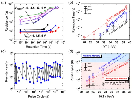
Long-term device reliability characteristics, such as reten-tion time and endurance, are critical for SCM applicareten-tions. The planar shadow-mask devices were used in this investigation because they are less prone to unoptimized process variations in the V-RRAM, thus facilitating the collection of statistical data with high confidence. Figure5(a) shows the typical reten-tion failure behavior of the MIIM self-rectifying cell at room temperature. Multiple LRSs and HRSs were programmed by dc SET and RESET operations, respectively, at various voltages. Both the LRS and HRS resistances increased as the retention time increased, eventually saturating in a much higher resistance state of 1 G. Therefore, we defined the retention failure criterion as the point when the LRS resistance increases by a factor of ten and becomes indistinguishable from the lowest HRS resistance before performing the retention test.
Nanotechnology25 (2014) 165202 C-W Hsu et al
Figure 5. In a shadow-mask Ta/TaOx(10 nm)/TiO2(30 nm)/Ti MIIM, (a) typical retention failure behaviors of the LRSs obtained by
varying SET voltages and the HRSs obtained by varying RESET voltages at room temperature. (b) Arrhenius plot of the LRS retention time as a function of SET voltage. Retention failure is defined as occurring when the LRS resistance increased by a factor of ten. (c) Typical pulse endurance of over 1012cycles achieved using ac SET and RESET pulses of 100 ns at ±6 V and a read voltage of −2 V at room temperature. (d) Arrhenius plot of the endurance cycle as a function of the magnitude of SET pulses of 100 ns. A fixed RESET pulse of 100 ns at −6 V was used.
The resistance increase may be explained by the increase in the tunnel width of the Ta/TaOx Schottky barrier as O2−diffused away from the interface possessing a high O2−concentration into the TaOxfilm even with no external electric field present. Figure5(b) shows the Arrhenius plot of the LRS retention time obtained at varied SET voltages and baking temperatures from 25 to 175◦C. Thirty cells under each condition were measured. Using higher SET voltages yielded slightly lower LRS resis-tances and improved retention time because additional O2− was driven toward the Ta/TaOx interface. Furthermore, the extracted activation energy of O2−migration, EA≈0.7 eV, was relatively insensitive to SET voltage. All of the other devices with various TaOx/TiO2thicknesses produced a sim-ilar EA value (figure S4, supporting information available at stacks.iop.org/Nano/25/165202/mmedia). This EA value agrees with that used in the 1D O2− migration model, thus supporting the O2−diffusion mechanism for retention failure. Figure5(c) shows the typical endurance characteristics of the MIIM self-rectifying cell at room temperature on using ac SET and RESET pulses of 100 ns, which is close to the access time requirement of DRAM and may be further improved by optimizing the RC delay in the vertical RRAM structure. Higher pulse amplitudes than dc SET and RESET voltages were used because of the shorter pulse time. An extremely high endurance of over 1012 cycles without device wear-out is on a par with that of the best RRAM device previously reported [37]. For DRAM-like SCM applications, excellent device endurance must be guaranteed in a worst-case scenario
of a non-stop operating condition for ten years (i.e., endurance of over 1015cycles for a pulse width of 100 ns). We performed an acceleration test using elevated temperatures to project a device endurance beyond 1012 cycles. Figure 5(d) shows the Arrhenius plot of the endurance cycle obtained at varied SET pulse magnitudes and baking temperatures from 150 to 250 ◦C. Ten cells under each condition were measured. All of the failed devices remained in an LRS of 200 , which was much lower than that of the initial LRS, and were completely lacking in self-rectifying behavior, which is similar to the characteristics of a normal RRAM device after undergoing electrical forming. Therefore, we attributed the failure mode to the irreversible hard breakdown of the rectifying TaOx/TiO2interface. Although using a high SET voltage improves retention time, it degrades device endurance. A SET pulse of 8 V easily destroyed the interface within tens of cycles, whereas 1015 endurance cycles at 100 ◦C may be achieved by lowering the SET pulse to 6 V. The extracted activation energy of irreversible breakdown, EA0, shown in figure5(d), was much higher than the EA of O2− migration, indicating that the irreversible hard breakdown was not induced by the migration of existing O2−but rather by the generation of new O2−and VO defects near the TaOx/TiO2 interface under electrical stress. A much higher value of EA0 compared with that of EA is required to ensure robust device endurance. As shown in figure 5(d), the apparent voltage dependence on the time to irreversible hard breakdown and E0A also agrees with the occurrence of a dielectric
various SET voltages depending on their applications. For example, by applying a lower SET voltage, a working memory with an unlimited endurance but a retention time of minutes to hours could be a low-power alternative to volatile DRAM. By applying a higher SET voltage, a nonvolatile storage cache with a limited but reasonable endurance and a retention time of hours to days could expedite the slow process of acquiring data directly from disk drives and considerably reduce energy consumption. Furthermore, this SCM technology is compat-ible with 3D V-RRAM technology, which exhibits superior scalability, thereby ensuring an extremely low bit cost. 4. Conclusions
In summary, we present a promising SCM technology based on a TaOx/TiO2 V-RRAM structure and a homogeneous barrier modulation mechanism. The remarkable properties demonstrated in this device differ substantially from those of the prevalent filamentary RRAM, including a high self-rectifying ratio at a low operating current, negligible cycling variation, forming-free and self-compliance characteristics, and an extremely high endurance, capable of realizing work-ing memory applications. Therefore, this class of homoge-neous barrier modulation RRAM is optimal for realizing high-performance and ultra-high-density SCM and is, thus, deserving of more attention in future RRAM research. Several aspects of device fabrication and materials require further investigations. For example, other conformal deposition tech-niques such as atomic layer deposition (ALD) would benefit the thickness scaling of the RS films and the pitch-size scaling of 3D arrays; however, this may require developing substoi-chiometric ALD films. In addition, improvements in retention time might be possible by tailoring the TaOx compositions or inserting barrier layers to suppress O2−diffusion. Device scalability below 10 nm and the further reduction of operating voltages should also be investigated.
Acknowledgments
This work was supported by National Science Council of Taiwan, Republic of China, under grant NSC 101-2221-E009-089-MY3 and NSC 102-2221-E-009-188-MY3, and Winbond Electronics Corporation, Taichung, Taiwan. T-H Hou acknowl-edges support by the NCTU-UCB I-RiCE program, under grant NSC-102-2911-I-009-302. The authors are grateful to Wen-Yueh Jang and Chen-Hsi Lin of Winbond Electronics Corporation for valuable discussions, and the Nano Facility Center at National Chiao Tung University and National Nano Device Laboratories, where the experiments in this paper were performed.
[6] Xiong F, Bae M-H, Dai Y, Liao A, Behnam A, Carrion E, Hong S, Ielmini D and Pop E 2013 Nano Lett.13 464
[7] Beck A, Bednorz J G, Gerber C, Rossel C and Widmer D 2000 Appl. Phys. Lett.77 126902
[8] Waser R and Aono M 2007 Nature Mater.6 833
[9] Meijer G I 2008 Science319 1153909
[10] Waser R, Dittmann R, Staikov G and Szot K 2009 Adv. Mater.
21 2632
[11] Yang J J, Borghetti J, Murphy D, Stewart D R and Williams R S 2009 Adv. Mater.21 3754
[12] Yang J J, Strukov D B and Stewart D R 2013 Nature Nanotechnol.8 13
[13] Kawahara A et al 2012 IEEE Tech. Dig. ISSCC p 432 [14] Kawahara A et al 2013 IEEE Tech. Dig. ISSCC p 220 [15] Liu T-Y et al 2013 IEEE Tech. Dig. ISSCC p 210 [16] Baek I et al 2011 IEDM Tech. Dig. p 737
[17] Chien W-C et al 2012 Tech. Dig. VLSI Symp. p 153 [18] Yu S, Chen H-Y, Gao B, Kang J and Wong H-S P 2013 ACS
Nano7 2320
[19] Prall K and Para K 2010 IEDM Tech. Dig. p 102 [20] Govoreanu B et al 2011 IEDM Tech. Dig. p 729 [21] Park S-G et al 2012 IEDM Tech. Dig. p 501
[22] Hsu C-W, Hou T-H, Chen M-C, Wang I-T and Lo C-L 2013 IEEE Electron Device Lett.34 885
[23] Hsu C-W, Wang I-T, Lo C-L, Chiang M-C, Jang W-Y, Lin C-H and Hou T-H 2013 Tech. Dig. VLSI Symp. p 166 [24] Linn E, Rosezin R, Kugeler C and Waser R 2010 Nature
Mater.9 403
[25] Lo C-L, Hou T-H, Chen M-C and Huang J-J 2013 IEEE Trans. Electron Devices60 420
[26] Zhang Y, Duan Z, Li R, Ku C-J, Reyes P, Ashrafi A, Zhong J and Lu Y 2013 J. Phys. D46 145101
[27] Chae S-C et al 2008 Adv. Mater.20 1154
[28] Luo W-C, Liu J-C, Lin Y-C, Lo C-L, Huang J-J, Lin K-L and Hou T-H 2013 IEEE Trans. Electron Devices60 3760
[29] Goux L et al 2013 Tech. Dig. VLSI Symp. p 162
[30] Guan X, Yu S and Wong H-S P 2012 IEEE Trans. Electron Devices59 1172
[31] Szot K, Speier W, Bihlmayer G and Waser R 2006 Nature Mater.5 312
[32] Kwon D-H et al 2010 Nature Nanotechnol.5 148
[33] Yang J J, Pickett M D, Li X, Ohlberg D A A, Stewart D R and Williams R S 2008 Nature Nanotechnol.3 429
[34] Liu Q, Sun J, Lv H, Long S, Yin K, Wan N, Li Y, Sun L and Liu M 2012 Adv. Mater.24 1844
[35] Huang J-J, Kuo C-W, Chang W-C and Hou T-H 2010 Appl. Phys. Lett.96 262901
[36] Zhuo V Y-Q, Jiang Y, Li M H, Chua E K, Zhang Z, Pan J S, Zhao R, Shi L P, Chong T C and Robertson J 2013 Appl. Phys. Lett.102 062106
[37] Lee M-J et al 2011 Nature Mater.10 625