國立交通大學
光電工程研究所
碩 士 論 文
官能基修飾有機薄膜電晶體氣體感測
之研究
Functional Group Modification on
Dielectric Interface of Pentacene-Based
OTFTs for Ammonia Sensing Application
研 究 生:吳權陵
指導教授:冉曉雯 博士
中華民國 九十七年八月
官能基修飾有機薄膜電晶體氣體感測之研究
研究生:吳權陵 指導教授:冉曉雯 博士
國立交通大學
光電工程研究所碩士班
摘要
在此論文中,我們藉由修改官能基來得到有機薄膜電晶體(OTFTs) 氣體變化 感覺能力。利用自組裝單層膜(SAM)的方式,在氧化曾上分別修飾了三氨碁丙基三 乙氧基硅烷以及十八烷基三甲氧基硅烷.由於三氨碁丙基三乙氧基硅烷以及十八 烷基三甲氧基硅烷都是疏水層,因此會造成低表面能以利於五環素成長.因此氧化 層與pentacene間的表面性質已經改變.而藉著改變表面態後的OTFTs來當作氣體 感測器.對於氣體感應器, 在我們的之前的研究,四點探針的方法用來研究寄生電 阻以及薄膜電阻的改變.同時也顯示出,經過表面處理修飾後,pentacene薄膜電阻變 化似乎已經變成主要因素,對於氣體感應而言.但是,寄生電阻是影響氣體感應的 控制因素。相反結果,也可能由不同的SAMs解釋導致pentacene 結構或薄膜載子密 度, 進而影響OTFTs 與氣體間的反應。另外, 多個參數,譬如載子遷移率、臨界電 壓, 和次臨界擺幅並且使用分析氣體感應互作用。基於在這個結果下, 我們證明 怎麼增加對專一氣體的感應能力,在藉由官能基修飾氧化層的方法下。在羅淵仁 學長以及周政偉學長的指導下,一起合作進行此研究。Functional Group Modification on Dielectric Interface of
Pentacene-Based OTFTs for Ammonia Sensor
Application
Student:Chuan-ling Wu Advisor:Dr. Hsiao-Wen Zan
Institute of Electro-Optical Engineering
National Chiao Tung University
Abstract
IN this thesis, we modify the functional groups to obtain diversity of organic thin-film transistors (OTFTs) gas sensing ability. By using self-assembled monolayer (SAMs) treatment, the silicon oxide surface (SiO2) was modified by 3-amino-propyltriethoxysilane (APTES) and n-octadecyltrimethoxysilane (ODMS). Both ODMS and APTES (with amine groups) were hydrophobic, which served a low surface-energy surface for pentacene film growth. Therefore, the interface properties between pentacene film and SiO2 will be significantly changed. The OTFTs with interface modifications was then used as gas sensors. During gas sensing, in our previous reports, the gated-four-probes method was also used to analyze the changes of contact resistance and pentacene-film resistance. It was shown that with interface modifications, pentacene film resistance variation will become a key factor in gas sensing. However, the contact resistance was dominated factor that influenced gas
sensing. The contrary results can be explained by the different SAMs will result in different pentacene structure or thin-film carrier density, which influenced the OTFTs interaction to gases. Additionally, multiple parameters such as mobility, threshold voltage, and sub threshold swing were also used to analyze gas sensing interactions. Base on this result, we prove how to increase sensing ability of a specific material with functional groups modification on silicon oxide interface. In Cwei-Chou and Yuanren Lo’s instruction, we cooperate together and finish this research.
誌謝
兩年的時間過的很快,回首兩年前,滿懷著夢想與期望來到交大。在交大的求 學過程中,遇到了許多的考驗,這些考驗使自己在思想或能力上都成長許多。首 先要感謝我的指導教授冉曉雯老師,感謝冉老師帶領我進入OTFT 的世界,以及 在研究路上不厭其煩的指導我。 感謝實驗室的博班學長:國錫學長、政偉學長、士欽學長,以及 楊裕雄實驗 室的羅淵仁學長,在這兩年來的幫助與鼓勵。尤其是政偉學長以及淵仁學長,在 我這兩年來的研究生涯裡,用心的教導我實驗方法並且辛苦地協助我完成我的碩 士論文。感謝實驗室的同學:俊傑、志宇、旻君、武衛、和璁,這兩年來的互相 打氣,互相砥礪。感謝實驗室的學弟妹們:淑玲、玉玫、鈞銘、慶能、達欣、威 豪、建民、芳弘、煥之…等,在苦悶的研究生活裡,添加了許多歡樂。 最後感謝我的父母、弟弟以及女友,感謝你們一路的陪伴與支持,沒有你們, 就不會有今日的我。Contents
Abstract (Chinese)
Ι
Abstract (English)
II
Acknowledgement
IVContents
V
Table Captions
VII
Figure Captions
VIII
Chapter 1. Introduction
1-1 Introduction of Organic Thin Film Transistors (OTFTs) 1
1-2 Organic semiconducting materials and the transport mechanism 2
1-3 Surface treatment 8
1-4 OTFT for gas sensing 9
1-5 Motivation 10
1-6 Thesis Organization 10
Chapter 2. OTFT for gas sensing
2-1 Brief review 14
2-2 Sensing mechanisms 15
2-2-1 Morphology effect 2-2-2 Contact effect on nano-length devices 2-2-3 Sensing Selectivity
2-3 Immobilization of Bio-molecules 17
Chapter 3. Experiments Methods
3-1 Device structures and fabrication 22
3-1-1 Gated four-probes OTFTs for resistance measurement 3-1-2 Preparation of Substrates 3-1-3 Surface treatment 3-1-4 Growth of Thin Film and Electrodes
3-2 Measurement Methods and Parameters extraction 25
3-2-2 Threshold voltage 3-2-3 On/Off current ratio 3-2-4 Subthreshod swing
3-2 Gas-Sensing system 27
Chapter 4. Result and Discussion
4-1 SAM with APTES/ODMS 32
4-1-1 Percentage control 4-1-2 Molecule Immobilization
4-2 Material and electrical analysis on SAM-OTFTs 33
4-2-1 AFM analysis of SAM quality 4-2-2 Electrical Characteristics of OTFTs with distinct SAM-dielectrics
4-3 Effects of ammonia (NH3) on Gated four-probe SAM-OTFTs 35
4-3-1 Id-Vg curve variation 4-3-2 Contact resistance variation 4-3-3 Threshold voltage and mobility variation
Chapter 5. Conclusion and Future work
5-1 Conclusion and future work 54
References
56Profile
63Table Captions
Table I Summary of reviewed OFET sensors
Table II The surface roughness of ODMS, ODMS mixed with APTES, APTES-dipped SiO2
Figure Captions
Chapter 1
Fig. 1.1 The applications of plastic transistors: flexible displays, smart cards, RFID
tags.
Fig. 1.2 Semilogarithmic plot of mobility vs. year.
Fig. 1.3 Molecular structure of (a) sexithiophene and (b) pentacene.
Fig. 1.4 Energy band diagram of pentacene
Fig. 1.5 Chemical structure of APTES and ODMS - SAMs
Chapter 2
Figure 2.1. Sensing data of Ids (normalized to that measured just before the analyte
was delivered) for 80 nm pentacene grain size and different nanoscale channel lengths (same W/L of 10), measured at Vg =Vds=Vside=−2.5 V (two side guards were kept at the same potential as the drain), d distance from syringe nozzle to devised=2 mm, v analytic fluxd =45 ml/min
.
Figure 2.2 Map illustrating the effect of 16 analytes on 11 sensor materials. Black
indicates that data are not available and white indicates negligible response. Positive changes in sensor current are shown in shades of blue while decreases are shown in shades of red.
Chapter 3
Figure 3.1. (a) Top view of a field-effect device. (b) Schematic voltage drop along the
channel for an OTFT biased in the linear region of device operation. The potential drop between the voltage-probing electrodes is assumed to be linear for the evaluation of the mobility from the four-terminal measurement.
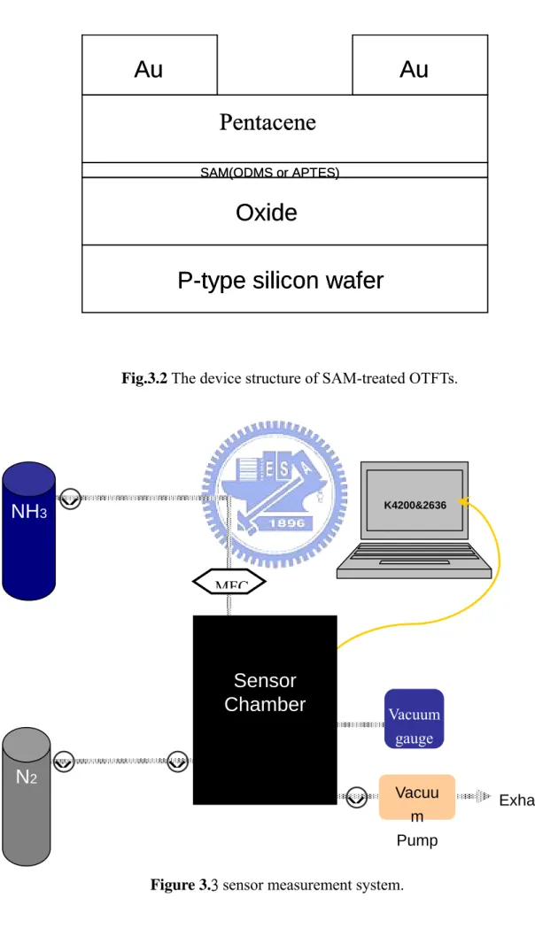
Fig. 3.2 The device structure of SAM-treated OTFTs.
Fig. 3.3 sensor measurement system.
Fig. 3.4 analyte controll system.
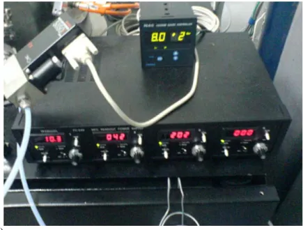
(a)There is a four channel Mass Flow Controller (MFC) Readout Power Supply,and a vacuum gauge.
(b) There is a Mass Flow Controller
Fig. 3.5 Chamber used for sensor experiments.
Chapter 4
Fig.4.1 The contact angle of the de-ionized water on ODMS-treated SiO2 surface, and
on APTES-treated SiO2 surface, respectively.
Fig.4.2 (a) The amine groups of APTES can covalent bonding with anti-body. (b) The amine groups of APTES can covalent bonding with bovine serum
albumin (BSA)
(c) Atomic force microscope (AFM) images of SAM-dipped SiO2 dielectric
for ODMS and APTES
(d) pentacene AFM image on SAM-dipped SiO2 layer for ODMS and APTES
Fig.4.4 (a)Electrical characteristics of ODMS-OTFTs in 0.5ppm NH3 in 5mins,
10mins, and 20mins.
(b)Electrical characteristics of APTES-OTFTs in0.5ppm NH3 in 5mins,
10mins, and 20mins
Fig.4.5(a)field-effect mobility and threshold voltage of ODMS-OTFTs in 0.5ppm
NH3 in 5 mins,10mins,and 20mins.
(b)field-effect mobility and threshold voltage of APTES-OTFTs in 0.5ppm
NH3 in 5 mins,10mins,and 20mins.
Fig.4.6 (a) Electrical characteristics of ODMS-OTFTs in NH3.
(b)Electrical characteristics of APTES-OTFTs in NH3.
(c) the change of maximum on drain-current (I ) of ODMS D and APTES-OTFT versus NH3 concentration
Fig.4.7 TheRcontand Rfilmare plotted as a function of gate-voltage minus threshold-voltage (VG−Vth), respectively.
Fig. 4.8 (a) For ODMS-OTFTs, the percentage (%) of Rcont and Rfilm versus injected NH3.
(b) For APTES-OTFTs, the percentage (%) of Rcont and Rfilm versus injected NH3.
Fig. 4.9 The threshold voltage shift (ΔVth) of ODMS and APTES-OTFTs is plotted as a function of NH3 concentration.
Fig. 4.10 The field-effect mobility of ODMS and APTES-OTFTs is plotted as a
function of NH3 concentration.
Fig. 4.11 The subthreshold swing (S S. .) of ODMS and APTES-OTFTs is plotted as a function of NH3 concentration.
Chapter 1
Introduction
1.1 Introduction of Organic Thin Film Transistors (OTFTs)
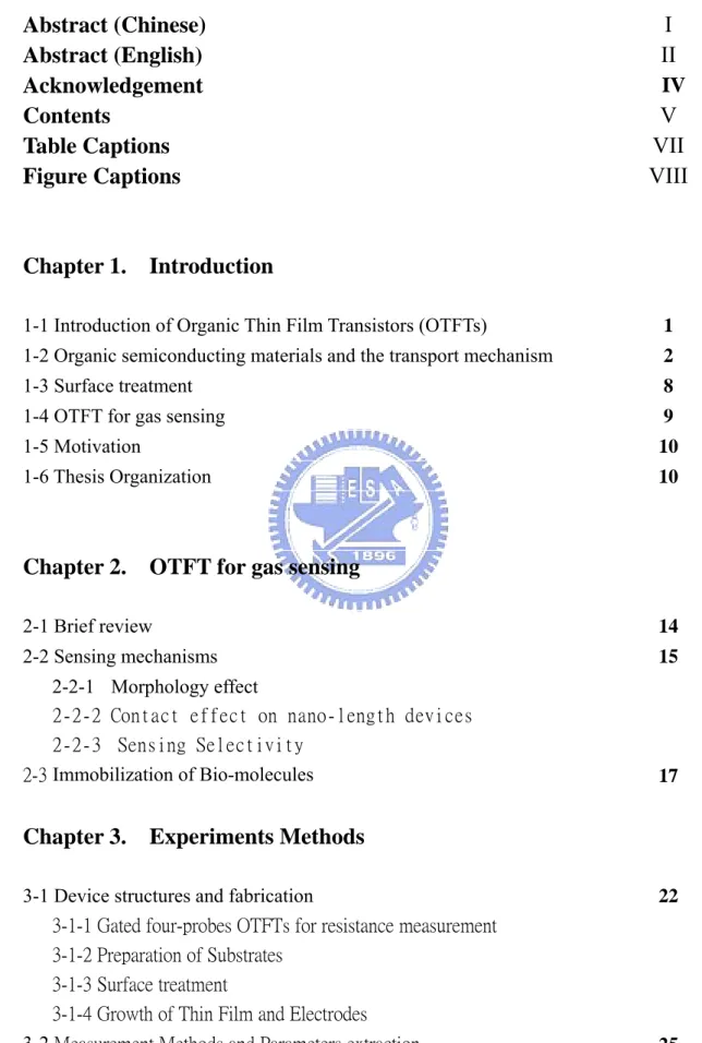
“Plastic transistors” open the future of flexible displays, smart cards, radio frequency (RF) identification tags, as well as light-emitting diodes (LED) and lasers [1]. Rapid progress in this field has been achieved by improving the material properties and the process techniques.
As for the application of electronics, the organic active layer has attended a mobility of 1cm2/Vs and a switching speed of 108 Hz, which is comparable to
amorphous hydrogenated silicon (a-Si:H)[2]. Since the late 1940s, there has been a lot of research on the development of organic semiconductor [3]. These organic semiconductors are small molecules and polymers, which have alternative single or double-bond in common. This is because of the large π-conjugation length along the long axis of the molecules and closed π-stacking are the key factors of high carrier mobility [3].
Similar to inorganic semiconductors, organic ones can function as p-type or n-type. However, most reported high-mobility organic semiconductors are p-type material. Among the p-type material, pentacene (C14H22), a rod-like aromatic
owning to highly ordered films with proper dielectric properties and growth conditions[4].
1.2 Organic semiconducting materials and the transport mechanism
Organic materials such as polythiophene, α- sexithiophene (α-6T) have been investigated for use in field effect transistors (FETs) [5]. Polycrystalline molecular solids such as α-sexithiophene (α-6T) or amorphous/semi-crystalline polymers such as polythiophene or acenes such as pentacene, teracene show the highest mobility [6]. Figure 1.2 shows the evolution of organic materials and the improvement in their mobility over the years [7]. Pentacene based FETs show the high mobility and have been extensively studied. Pentacene is made up of five benzene rings as shown in Fig. 1.3 .Pentacene has a sublimation temperature of 300℃. Well ordered pentacene films can be deposited at low temperatures making it suitable for deposition on plastic substrates.Organic conjugated materials used in OTFTs can be generally divided into two groups. Among the semiconductors, one group is the polymers and the other is the oligomers. The polymers are formed by a repeating chain of hydrogen and carbon in various configurations with other elements, but they have relatively poor mobilities (4X10⁻²cm2/Vs [8]). The oligomers are held together by weak Van der Waal forces
higher mobilities (1.5 cm2/Vs [9]). The organic materials can function either as p-type or n-type. In p-type semiconductors, the majority carriers are holes; while in n-type the majority carriers are electrons. Among, p-type semiconductors are the most widely studied organic semiconductors. Recently, many molecular semiconductors, such as pentacene, thiophene oligomers, and regioregular poly(3-alkyl-thiophene) are proposed. The pentacene (C22H14) is a promising candidate for future electronic
devices and an interesting model system, due to its superior field effect mobility and environmental stability [10].
Pentacene is one of the popular materials in OTFTs. Its mobility has reached the fundamental limit (>3cm2/Vs) [11, 12] which is obtained with a single crystaline
at room temperature. The mobility of pentacene is comparable to that of amorphous silicon which is widely developed and used in active matrix liquid crystal displays (AMLCD) and the other electronic applications.
Pentacene is an aromatic compound with five condensed benzene rings and therefore, the chemical formula is C22H14 with molecular weight 278.3. The volume of the unit
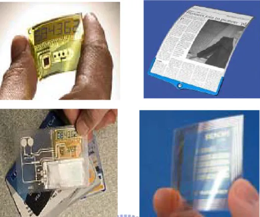
cell is about 705Å [11]. The permittivity is 4[12], and the electron affinity is about 2.49eV. Silinish et al. determined the adiabatic energy gap ( Ad
G
E ) by using the threshold function of intrinsic photoconductivity in pentacene[13]. The second transition is from the excited state to the ionic state, which is called the optical energy
gap ( Opt G
E ). According to Fig. 1.4, the adiabatic energy gap as 2.47eV and the optical energy gap as 2.83eV are recorded [14]. Pentacene is used as an active layer. Its purity leads to longer diffusion length for the charge transporting with less interaction with the lattice. Furthermore, the impurities in the material tend to chemically combine with the organic semiconductor material which leads to irregularities in the band gap [15]. Therefore, the thermal evaporation is carried out under high or ultra high vacuum conditions to avoid the impurities and increase the quality of the material. It is well known that the deposition temperature, deposition pressure, and deposition rate are the three critical parameters to the organic film quality. Lower deposition rate and appropriate deposition temperature is expected to result in better ordering of the organic molecules, thin-film phase formation of pentacene film, and the better performance [16]. In OTFTs, the roughness has a influence on the morphology, whereas the films on the smooth thermal oxide are in generally highly ordered. The surface chemistry also is a typical issue to organic devices. Changing surface wettability as a hydrophobic surface by surface treatment leads to mobilities increasing [17].
Carrier transportation in the organic semiconductors have been investigated on the theory and modeling in the past years [18]. Recently, two principal types of theoretical model are used to describe the transport in organic semiconductors: “The
band-transport model” and “The hopping models”. However, band transport may not suit for some disordered organic semiconductors, in which carrier transport is govern by the hopping between localized states. Hopping is assisted by phonons and the mobility increases with temperature. Typically, the mobility is very low, usually much lower than 1cm2/V-sec. The boundary between “band transport” and
“hopping” is divided by materials mobilities (~1cm2/V-sec) at room-temperature (RT)
[19]. Many kinds of polycrystalline organic semiconductors, such as several members of the acene series including pentacene, rubrene, have RT mobility over the boundary [20]. Sometimes, temperature-independent mobility was found in some polycrystalline pentacene devices [21]. Thus, this observation argued that the simply thermal activated hopping process governed the whole carrier transport behaviors in high quality polycrystalline pentacene film; despite that the temperature independent mobility has been observed in exceptional cases [21].
Finally, the exact nature of the charge carrier transport in organic molecular crystals is still not well-understood, which has been the focus in many theoretical studies [22].
In the past 20 years, a great deal of progress has been made in improving the
field-effect mobilities of OFETs [23].It has also been demonstrated that the properties
crystalline structure, where the π delocalized carriers are responsible for the intra-molecular conduction.However, the nature of van der Waals bonding between discrete molecules is thought to be the limitation of the carrier transport, and the transport is usually described by “localized model. Thus, the charged carrier transport must be described by different models than those in covalently bonded semiconductors.
Recently, two principal types of theoretical model are used to describe the transport in organic semiconductors: “The band-transport model” and “The hopping models”. However, band transport may not suit for some disordered organic semiconductors, in which carrier transport is govern by the hopping between localized states. Hopping is assisted by phonons and the mobility increases with temperature. Typically, the mobility is very low, usually much lower than 1cm2/V-sec. The
boundary between “band transport” and “hopping” is divided by materials mobilities (~1cm2/V-sec) at room-temperature (RT) [24]. Many kinds of polycrystalline
organic semiconductors, such as several members of the acene series including pentacene, rubrene, have RT mobility over the boundary [25]. Sometimes, temperature-independent mobility was found in some polycrystalline pentacene devices [26]. Thus, this observation argued that the simply thermal activated hopping process governed the whole carrier transport behaviors in high quality
polycrystalline pentacene film; despite that the temperature independent mobility has been observed in exceptional cases [27].
The understanding of carrier transport in single-crystal of organic semiconductors will help us to describe the transport mechanism in polycrystalline organic semiconductors. The coherent band-like transport of delocalized carriers becomes the prevalent transport-mechanism in the single crystals of organic semiconductors, such as pentacene, tetracene, under the low-temperature environments. A very high hole mobility values has been measured by time-of-flight experiments. Thus, the temperature dependence of the carrier mobility was found below 100K and following with a power law of
μ
∝ T-n, n~1,, in singlecrystals of organic semiconductors, consistent with the band-transport model. However, between 100K and 300K, the carrier mobility show a constant value, that has been described as the superposition of two independent carrier transport mechanisms. The first mechanism was small molecular polaron (MP). According to this model, the carriers were treated as the heavy; polaron-type; quasi-particles. It is formed by the interaction of the carriers with intra-molecular vibrations of the local lattice environment, and move coherently via tunneling. In this model, the mobility follows the power law
μ
MP=aT-n. The other involves a small lattice polaron (LP),dependence of mobility on temperature:
μ
LP=bexp[-Ea/kT]. The superposition ofthese two mechanisms could get a good consistence with experimentally measurement of temperature-dependence mobility from room temperature to Kelvin degrees (K).
Finally, the exact nature of the charge carrier transport in organic molecular crystals is still not well-understood, which has been the focus in many theoretical studies.
1.3 Surface treatment
Several researchers had verified the hydrophobic surface was more suitable for organic film deposition [28]. Since the hydrophobic polymer dielectric has lower or similar surface energy to organic films. The similar concept was also realized by self-assembled monolayer (SAM) on inorganic dielectrics. If the inorganic dielectrics with lower surface-energy, that may provide better performance and resulted in lower interface traps in OTFTs [29]. The surface properties such as frictional or abrasion, permeability, insulating properties, wettability and chemical reactivity are strongly dependent on a molecular aggregation state of the surface [30, 31]. Therefore, the control of a molecular aggregation state on the film is important to construct a highly functionalized surface. One of the most effective ways of studying surface properties is contact angle measurement. The contact angle is the angle
between the tangent to the drop’s profile and the tangent to the surface at the intersection of the vapor, the liquid, and the solid. The contact angle is an index of the wettability of the solid surface. A low contact angle between solid surface water-drop indicates that the surface is hydrophilic and has a high surface energy. On the contrary, a high contact angle means that the surface is hydrophobic and has a low surface energy. The surface free energy was traditionally quantified by contact angle measurements [32, 33].
In this study, we fabricated the electrical properties of the OTFTs using pentacene fabricated by thermal evaporation in high vacuum with the two kinds of dielectric surface treatment material - (octadecyltrimethoxysilane, ODMS) and (3-Aminopropyltriethoxysilane, APTES) (see Fig. 1.5).
1.4 OTFTs for gas-sensing
For the next generation of sensor applications on medical diagnostics, food monitoring, and chemical or biological warfare etc.; portable, low cost, and low power-consumption will be important demands. As for these demands, the OTFT should be an important candidate due to its flexibility and its simple fabrication process. Therefore, the studies of organic thin-film transistors (OTFTs) to physical, chemical [34], and biological sensors [35] will become an important object.
gaseous species, five parameters: the turn-on current (I ), the turn-off current (on Ioff), the threshold-voltage (V ), the field-effect mobility (th μeff ) and the subthreshold-swing (S S. .), are used to estimate the gaseous interaction in OTFTs. By this way, a
“multi-dimensional” gas sensor can be realized as a single OTFT.
1-5 Motivation
How to promote the sensing qualitative ability of OTFTs sensor is always an important topic. We propose modifying dielectric surface by different functional groups of SAM can change characteristics of gas sensing.
SAM was more hydrophobic and the surface free energy was similar to that of the pentacene film .Besides, we change the functional groups of SAM to change ammonia sensor ability. If we can obtain different gas sensing characteristics modified by different functional groups, we can attain the sensing qualitative ability.
1-6 Thesis Organization
In Chapter 1, we describe the introduction of OTFTs, Surface treatment and motivation of the thesis. In Chapter 2, we introduce sensing mechanisms, and immobilization of Bio-molecules. In Chapter 3, the fabrication and the structure of OTFTs, and parameter extraction are presented. In Chapter 4, Self-Assembly Monolayer (SAM) and surface energy, electrical properties of SAM-treated OTFTs, and effects of ammonia (NH3) on Gated four-probe OTFTs are investigated. Finally,
Figure 1.1 The applications of plastic transistors: flexible displays, smart cards, RFID
tags.
[Adapted from http://tech.sina.com.cn/digi/2006-04-20/1204911539.shtml]
Fig. 1.3 Molecular structure of (a) sexithiophene and (b) pentacene.
3-Aminopropyltriethoxysilane (APTES) octadecyltrimethoxysilane (ODMS)
Chapter 2
OTFTs for gas sensing
2-1 Brief Review
Organic thin-film transistors (OTFTs) offer a great deal of promise for applications in chemical and biological sensing. For a broad range of sensing applications (e.g.,medical diagnostics, food monitoring, detection of chemical, biological warfare agents, etc.), there is a demand for small, portable, and inexpensive sensors. OTFTs have many advantages over other types of sensors that may allow them to meet this need. Organic semiconductors can be deposited using low-temperature processes on a variety of substrates, including mechanically flexible ones. As a result, low-cost fabrication techniques can be used to produce OTFTs. Miniaturization of these devices is straightforward, so portability, small sample volumes, and arrays with many elements are achievable. In addition, they provide a response (current change) that is easy to measure with simple instrumentation. With these advantages, it is feasible that single-use, disposable sensors could be realized using OTFTs.
OTFTs can be roughly classified into two primary categories: organic field-effect transistors (OFETs) and organic electrochemical transistors (OECTs) (including ISOFETs) OECTs exhibit much lower operating voltages than OFETs, but due to the
movement of ions involved in OECTs, their switching times are considerably slower (on the scale of seconds or longer) than those for OFETs (on the scale of milliseconds or shorter).In this paper,[34]they show the chemical and biological sensors based on OTFTs.(see Table I)
2-2 Sensing Mechanisms
2-2-1 Morphology effect
Grain boundaries (GBs) play a critical role in OFET sensing. The grain size of
the corresponding film was varied by changing the substrate temperature during
deposition. According to the images from transmission electron microscope (TEM)
from different substrate temperatures, Torsi et al. indicate thatthe response is strong for the low-temperature film one, which has more grain boundaries. However, the response is weak for the high-temperature one, which has fewer grain boundaries and a more compact structure. That implies for alcohols, the response of the sensor depends on interaction at grain boundaries. [36]
2-2-2 Contact effect on nano-length devices
The modeling for the mechanism of the sensing response will be published elsewhere. [37]Here, the reference briefly proposes the concept of the sensing mechanism of polycrystalline organic thin-film dependent on the channel length relative to grain sizes. In the organic semiconductor layer, both grains and grain
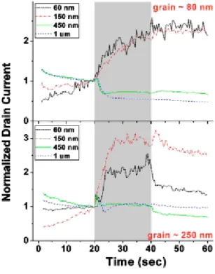
boundaries could be affected by the analyte molecules. Due to their dipole nature, the analyte molecules airborne on grain boundaries will trap the mobile charge carriers from the channel. [38] [39] Meanwhile the analyte (1-pentanol) interacting with the semiconductor (pentacene) grains will result in excess holes through chemical processes that are not completely understood. We propose that the overall sensing response is the result of a combination of these two competing effects. For a longer channel relative to grain sizes, there are enough grain boundaries inside the channel so that the former effect is dominant and the overall sensing response is the current decreasing (mobility reduced by the trapping effect at grain boundaries). For a shorter channel relative to grain sizes, the latter effect dominates due to very few number of grain boundaries inside channel, which leads to the current increasing by excess charges from the interaction between grains and the analyte.The result is shown in Fig. 2.1
2-2-3 Sensing Selectivity
To realize selective gas detection, sensor arrays are often constructed, i.e. several sensors showing different patterns of gas sensitivity are selected and simultaneously operated. Signal evaluation algorithms ranging from partial least squares methods to neural networks with fuzzy preprocessing are used to identify the
type of gases presented and to calculate their concentrations. A simple technique to obtain an array using one sensor is to modulate the operating temperature to different define levels.
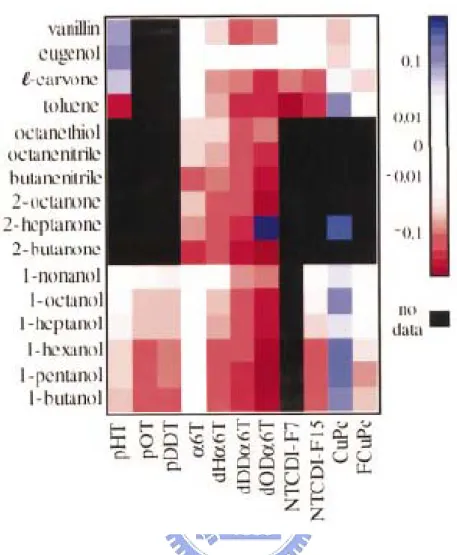
In the research of Crone et al. [40], they adopt eleven different organic thin films to make OTFT and observe the reaction of these OTFTs to sixteen different gases. The result is shown in Fig. 2.2 and it also reveals that OTFTs apply to electronic nose. Then, in 2005 year Liao et al. submitted that concept of application of OTFTs on electronic nose. [41] They proposed three different active materials including P3HT, pentacene, and P3OT to make OTFTs and show the sensing gas selectively for these OTFTs.
2-3 Immobilizations of Bio-molecules
Self-assembled monolayer (SAM) technology provides a powerful tool for generating monolayers of biological molecules on various substrates. The formation of such monolayers offers great versatility in terms of the sophisticated bio-recognition, which might provide a method for the in vitro development of biosurfaces that are able to mimic naturally occurring molecular recognition process [42]. SAMs also permit reliable control over the packing density and the environment of an immobilized recognition center or multiple centers on a substrate surface [43].
In the paper, they demonstrate a novel DNA hybridization detection method with organic thin film transistors.[44] DNA molecules are immobilized directly on the surface of organic semiconductors, producing an unambiguous doping-induced threshold voltage shift upon hybridization. With these shifts, single-stranded DNA (ssDNA) and double-stranded DNA (dsDNA) are differentiated successfully.
In our research, we try to immobilize BSA on the SAM treated surface, and observe that BSA bond with APTES .Then, we make OTFTs treated by SAM to sense gas and try to increase the sensing selectivity of OTFTs for ammonia. Finally, we expect to immobilize DNA on the SAM treated surface and detect Biological member.
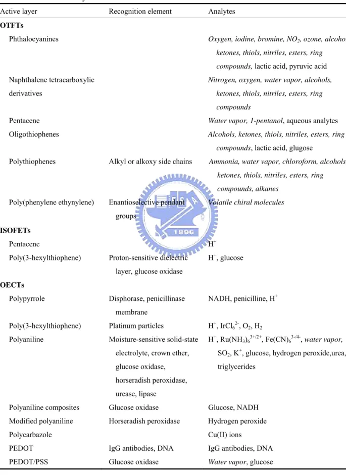
Table I Summary of reviewed OFET sensors
Active layer Recognition element Analytes
OTFTs
Phthalocyanines Oxygen, iodine, bromine, NO2, ozone, alcohols,
ketones, thiols, nitriles, esters, ring compounds, lactic acid, pyruvic acid
Naphthalene tetracarboxylic derivatives
Nitrogen, oxygen, water vapor, alcohols, ketones, thiols, nitriles, esters, ring compounds
Pentacene Water vapor, 1-pentanol, aqueous analytes
Oligothiophenes Alcohols, ketones, thiols, nitriles, esters, ring compounds, lactic acid, glugose
Polythiophenes Alkyl or alkoxy side chains Ammonia, water vapor, chloroform, alcohols, ketones, thiols, nitriles, esters, ring compounds, alkanes
Poly(phenylene ethynylene) Enantioselective pendant groups
Volatile chiral molecules
ISOFETs
Pentacene H+
Poly(3-hexylthiophene) Proton-sensitive dielectric layer, glucose oxidase
H+, glucose
OECTs
Polypyrrole Disphorase, penicillinase membrane
NADH, penicilline, H+ Poly(3-hexylthiophene) Platinum particles H+, IrCl
62-, O2, H2
Polyaniline Moisture-sensitive solid-state electrolyte, crown ether,
glucose oxidase, horseradish peroxidase, urease, lipase
H+, Ru(NH
3)63+/2+, Fe(CN)63-/4-, water vapor,
SO2, K+, glucose, hydrogen peroxide,urea, triglycerides
Polyaniline composites Glucose oxidase Glucose, NADH Modified polyaniline Horseradish peroxidase Hydrogen peroxide
Polycarbazole Cu(II) ions
PEDOT IgG antibodies, DNA IgG antibodies, DNA PEDOT/PSS Glucose oxidase Water vapor, glucose
Figure 2.1.Sensing data of Ids (normalized to that measured just before the analyte was
delivered) for 80 nm pentacene grain size and different nanoscale channel lengths (same W/L of 10), measured at Vg =Vds=Vside=−2.5 V (two side guards were kept at
the same potential as the drain), d distance from syringe nozzle to devised=2 mm, v analytic fluxd =45 ml/min.
Figure 2.2 Map illustrating the effect of 16 analytes on 11 sensor materials. Black indicates that data are not available and white indicates negligible response. Positive changes in sensor current are shown in shades of blue while decreases are shown in shades of red.
Chapter 3
EXPERIMENT METHODS
3-1
Device Structures and Fabrication
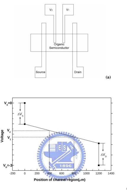
3-1-1 Gated four-probes OTFTs for resistance measurement
Gated four-probe OTFTs electrical measurements were carried out using a Keithley 4200-SCS semiconductor parameter analyzer. In the four-terminal measurements (Fig.3.1 (a)) the voltage drops V and 1 V between the source contact 2 and the two voltage-probing electrodes were measured separately, with two Kelvin-probes SMUs set current less then 10 14
Amps
− and measure the voltage. As shown in Fig. 3.1(b) (an idealized depiction of the change in potential through the device when biased in the linear region of device operation), the potential drop between the voltage probes is assumed to be linear for VDS <VGS −VT (where V T is the threshold voltage, VGS is the gate-source voltage, and VDS is the drain-source voltage), the field-effect mobility is given by
1 1 D i DS GS I L W C V V μ = × × × ∂ ∂ (1)
where C is the gate insulator capacitance per unit area about 3.45×10i -8 F/cm2. Knowing the channel potential at two points, V and1 V , a linear extrapolation of 2 the potential profile to each contact was performed. The potential drops at the source and drain, ΔVS , ΔVD and ΔVFilm , were calculated according to the following
equations: 1 2 2 2 2 1 ( ) ( ) ( ) S S V V V V L L V L L ⎡ − ⎤ Δ =⎢ − − ⎥− − ⎣ ⎦ (2) 1 2 2 2 2 1 ( ) ( ) D D V V V V V L L L ⎡ − ⎤ Δ = −⎢ + ⎥ − ⎣ ⎦ (3) 1 2 2 1 ( ) ( ) Film V V V L L L − Δ = − (4)
WhereV ,D V and 1 V are the voltages at the source, drain, and potential probes, 2 respectively.L ,1 L and L are the distances from the drain electrode to the first 2 potential probe, the second potential probe, and the source electrode, respectively. Where ΔVFilmis the actual voltage drop across the film.
With the knowledge of the total current flowing through the device and the potential drops across the film and contacts, the resistance of the source contact, drain contact, and the film can be calculated using Ohm’s Law, when devices operation in linear region. S S D V R I Δ = (5) D D D V R I Δ = (6) F F D V R I Δ = (7)
3-1-2
Preparation of SubstratesIn this study, the OTFT devices we used are top-contact structures. A p-type, single crystal silicon wafer (100) was used as the substrate and the gate electrode. After RCA cleaning, a 1000Å thermally-grown SiO2 layer was deposited by furnace.
After the SiO2 deposition, we try to remove the SiO2 layer from the wafer of
unpolished-side. The etching-solution we used is buffered oxide etching (B.O.E.) solution (40% NH4F and 1 part 49% HF). Hence, the wafer of unpolished-side
without SiO2 layer can serve as a gate-electrode. Finally, the substrate was cleaned
in ultrasonic tank by the sequence of: de-ionic water (5 minutes), acetone (1 minutes), and de-ionic water (5 minutes).
3-1-3 Surface Treatment
After substrate cleaning, we dip the octadecyltrimethoxysilane (ODMS) and 3-Aminopropyltriethoxysilane (APTES) individually unto the substrate. Consequently, we try to remove the residual solvent. The substrates are then baked in the oven at 120℃ about 15 minutes.
3-1-4 Growth of Thin Film and Electrodes
Pentacene, which was obtained form Aldrich Chemical Company without any purification, was used as an active layer. The deposition is started at a pressure lower than 3×10⁻⁶torr. The deposition rate is controlled at 0.5Å/s. The temperature we use in
depositing pentacene films is 70 oC. All the deposition parameters are monitored by a
quartz crystal microbalance (QCM) during the deposition process. In the end, a 1000Å Au layer was used as the source and drain pad, which is deposited at a rate of 1 Å/sec under 3×10⁻⁶ torr. The channel width (W) and length (L) defined by
shadow-mask was 800μm and 1200μm, respectively. Finally, the device is shown in Fig. 3.2.
3-2 Measurement Methods and Parameter Extraction
In this section, the methods of extraction the mobility, the threshold voltage, the subthreshod swing, the maximum interface trap density, and the is characterized, respectively.
3-2-1 Mobility
Generally, the linear mobility (forVD<VG−Vth) can be extracted from the transconductance maximum g in the linear region: m
OX D t cons V G D m V L WC V I g D μ = ⎥ ⎦ ⎤ ⎢ ⎣ ⎡ ∂ ∂ = = tan (2.5)
The saturation mobility (forVD>VG−Vth) can also be extracted from the slope of the curve in the squared drain-current versus the gate-voltage diagram:
( ) 2 OX G TH D C V V L W I = μ − (2.6) 3-2-2 Threshold voltage
We extract the threshold voltage from equation (2.6), the intersection point of the squared drain-current versus gate-voltage.
3-2-3 Subthreshod swing
Subthreshold swing is also important characteristics for device application. It is a factor to estimate how rapidly the device switches from the off state to the on state in the region of exponential current increase. It is defined by:
(
log)
=constant ∂ ∂=
D V D GI
V
S , when VG<VT for p-type.
Moverover, the subthreshold swing also represents the interface quality and the defect density [2], the maximum interface state trap-density can be extracted by:
q C q kT e S N i SS − ⋅ ⋅ = 1] / ) log( [
A high-performance TFTs will show a lower subthreshold swing.
3-2-4 On/Off current ratio
Devices with high on/off current ratio represent large turn-on current and small off current. It determines the gray-level switching of the displays. High on/off
current ratio means there are enough turn-on current to drive the pixel and sufficiently low off current to keep in low power consumption.
3-3 Gas-Sensing system
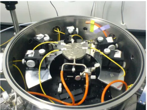
As shown in Fig. 3.3, the gas-sensing system consists of three major parts: a gaseous analyte controller, a gas-proof chamber, and a semiconductor parameter analyzer. In Fig. 3.4(a), (b), and (c), we show the mass flow controller, the power supply, and pressure gauge, respectively. The gaseous analyte was introduced into the gas-proof chamber via the mass flow controllers (MFC; 5850E, Brooks Instrument). The pressure inside the gas-proof chamber is monitored by vacuum gauge (PC-615). The total volume of the gas-proof chamber is about 40 liter. Fig. 3.5 is the top-view image of gas-sensing system. The system is equipped with five Kelvin-probes and positioners. The probes were connected to the semiconductor analyzer (Keithley 4200-SCS&2636) via tri-axial cables. The bottom pipe and the upper pipe serve as the gas-inlet and gas-exhaust, respectively. After mounting a metal cap with transparent window, the gas-proof chamber can be pumped down to less than 1 torr. Consequently, we introduce the pure nitrogen gas into the gas-proof chamber. Thus, all the gaseous-sensing experiments can be processed in a low-humidity and low-oxygen ambiance. All the experiments were also be operated at a pressure about 760 torr.
(a) -200 0 200 400 600 800 1000 1200 1400 VD=-3 VS=0 ΔVS ΔVD V2 V1
Position of channel region(μm)
Volta
g
e
(b)
Figure 3.1. (a) Top view of a field-effect device. (b) Schematic voltage drop along the channel for an OTFT biased in the linear region of device operation. The potential drop between the voltage-probing electrodes is assumed to be linear for the evaluation of the mobility from the four-terminal measurement.
P-type silicon wafer
Oxide
SAM(ODMS or APTES)
Pentacene
Au
Au
P-type silicon wafer
Oxide
SAM(ODMS or APTES)
Pentacene
Au
Au
Fig.3.2 The device structure of SAM-treated OTFTs.
Figure 3.3 sensor measurement system.
N
2 K4200&2636NH
3 MFC Vacuu m Pump×
×
×
×
Vacuum gaugeSensor
Chamber
Exhaust(a)
(b)
Figure 3.4 analyte control system.
(a) There is a four channel Mass Flow Controller (MFC) Readout Power Supply, and a vacuum gauge.
Chapter 4
Experiments Results and Discussion
4-1 SAM with APTES/ODMS
4-1-1 Percentage Control
Before identifying quality of SAM including ODMS and APTES, we try to mix ODMS and APTES. First, we must find the solvent including ethanol to dissolve ODMS and APTES. We observe that ethanol can dissolve both ODMS and APTES, but the sample must be overnight after dipping. Then, we change percentage of ODMS mixed APTES and the percentage are 100%ODMS, 90%ODMS/10%APTES, 50%ODMS/50%APTES, and 100%APTES, respectively.And, the percentage is volume ratio for ODMS and APTES.
4-1-2 Molecule Immobilization
The quality of ODMS and APTES immobilization can be approved by SEM, AFM, anti-body, and protein immobilization. The amine groups (-NH2) of APTES can
covalent bonding with anti-body, and anti-body is big molecular which has 10nm Au atom on the end so we can use SEM to check the growth condition of APTES. The result was shown in the inset of Fig. 4.2(a).In Fig. 4.2(a), we observe that Au atoms exist and the size of Au atom is about 10nm. But, the quantity of Au atom is too less so this method using SEM to check existence of BSA isn’t better.
Then, we use AFM to check the existence of BSA in Fig. 4.2(b). In Fig. 4.2(b), we deduced that protein truly draws in by APTES and not by ODMS. Besides, protein
on APTES is uniform and there is no protein on ODMS because there is no functional group on ODMS to covalent bond with BSA.We also deduced APTES truly grow on SiO2 because of AFM of BSA covalent bonded with APTES.Finally, we conclude that
the method of AFM of BSA can be observed more easily than the method of SEM of BSA.
4-2 Material ans electrical analysis on SAM-OTFTs
4-2-1 AFM analysis of SAM quality
By ODMS, ODMS mixed with APTES and APTES-dipped SiO2, we try to
initiate surface characteristics of SAM .In Fig. 4.2(b), we show the atomic force microscope (AFM) images of ODMS and APTES treated SiO2 dielectric. In the
Table III, as we can observe, we proposed ODMS, ODMS mixed with APTES, APTES and the surface roughness of ODMS, ODMS mixed with APTES including ODMS/APTES=90%/10% and 50%/50%, APTES-dipped SiO2 are about 0.234nm,
0.356nm, 0.369nm, and 0.221nm, respectively. APTES and ODMS have different numbers of carbon chain so the length of carbon chains between ODMS and APTES are different. We deduced the roughness of ODMS mixed APTES is bigger because the length of carbon chains between ODMS and APTES are different, and ODMS and APTES can’t match well to induce to broken bonds. Then we choose ODMS and APTES as our SAM in after research because ODMS mixed APTES-dipped SiO2 is
too rough. Additionally, we also understand that the ODMS and APTES will not affect the surface roughness of SiO2 significantly, so pentacene can grow on ODMS and
APTES treated SiO2 well. The AFM image of pentacene on SAM-dipped SiO2 layer is
also show in Fig. 4.2(c).It seems that the grain of pentacene on ODMS treated SiO2 is
bigger than that on APTES treated SiO2 because of surface energy difference between
ODMS and APTES treated SiO2 .
4-2-2 Electrical Characteristics of OTFTs with distinct SAM-dielectrics
Before ammonia is introduced into chamber, we compare electrical characteristics of ODMS and APTES-OTFTs including threshold voltage, mobility, and Subthreshold swing. After the source (Au), drain (Au), and voltage-probing electrodes are deposited on pentacene film, we measured the transfer characteristics of the gated-4-probes OTFT. The drain-current is plotted as a function of gate-voltage in Fig. 4.3.When gate bias changes from 5V to -50V and drain bias is -3V, the devices shows an on/off current ratio about 4 order for APTES-OTFTs and about 6 order for ODMS-OTFTs but the Ion~10-7A for ODMS and APTES-OTFTs are the same.
It also shows threshold voltage difference for ODMS and APTES-OTFT from -11.75 V to -43.6 V. The Vth difference may be attributing to –NH2 on APTES because of the
negative charge of-NH2 to trap the main carrier-hole. Mobility for ODMS and
between ODMS and APTES-OTFTs may be –NH2 on APTES to trap hole carriers.
Subthreshold swing for ODMS and APTES-OTFTs are1.34 and 1.73 V/decade, respectively. The Electrical Characteristics results show in the Table IV. We deduced –NH2 on APTES will trap hole and induced that the threshold voltage will
shift more negatively, on current, and mobility will get smaller, but it doesn’t affect Subthreshold swing a lot.
4-3 Effects of ammonia (NH
3) on Gated four-probe OTFTs
4-3-1 Id-Vg curve variation
Before the measurement, the gas-sensing chamber is pumped-down to less than 1 torr and vented to 760 torr by the high-purity nitrogen (N2) gas. Initially, we
measured the gated-4-probe OTFT in the nitrogen ambiance. Before ammonia (NH3)
is introduced into the chamber, we expected that ODMS and APTES-OTFTs are different in the change of threshold voltage shift and change of mobility because there is –NH2 on APTES and will be expected not to react with NH3.First, we analysis the
id-Vg curve of ODMS and APTES-OTFT in 5mins,10mins and 20mins in the 0.5ppm ammonia, and change gate bias from 5V to -45V and drain bias is fixed in -3V.We expect to observe that mobility and threshold voltage will saturate. The electrical characteristics of ODMS and APTES-OTFT are shown in Fig. 4.4(a) and 4.4(b). When the NH3 is introduced into the chamber, the drain-current (I ) will reduced D
from 5mins to 20mins. Interestingly, the threshold voltage will also shift more negatively, and field-effect mobility will decrease .But, we observe that the threshold voltage and mobility will saturate in 10mins in Fig. 4.5(a) and 4.5(b).So we decide to choose 10mins as our main parameter in our next experiment.
Then, we change the quantity of ammonia (NH3) from 0.5ppm to 1.5ppm. And,
we also change gate bias from 0V to -50V and drain bias is fixed in -3V. Then we measured the drain-current plotted as a function of gate-voltage every 10mins as the quantity of NH3 is 0.5ppm, 1ppm, 1.5ppm. In Fig. 4.6(a) and 4.6(b), when the NH3 is
introduced into the chamber, the drain-current (I ) will reduced with the increase of D the NH3 concentration in Fig. 4.6(c). The decrease of on current is because of
mobility or threshold voltage change by 2.6.In 4.3.3, we will analysis mobility and threshold voltage change with the increase of the NH3 concentration .Interestingly, the
threshold voltage will also shift more negatively, and field-effect mobility will decrease with the increase of the NH3 concentration. The on/off current ratio and the
subthreshold swing will not be changed significantly with the increase of the NH3
concentration.
4-3-2 Contact resistance variation
contact resistance and pentacene resistance by the gated-4-probe OTFT, respectively. From potential-probes on channel, the voltage-drops at the source electrode (Δ ), VS drain electrode (ΔVD), and within the pentacene film (ΔVfilm) can be estimated by:
2 1 1 1 2 1 ( ) [ ] ( ) S S V V V V L V L L − Δ = − ⋅ − − 2 1 2 2 2 1 ( ) [ ( )] ( ) D D V V V V V L L L L − Δ = − + ⋅ − − 2 1 2 1 ( ) ( ) film V V V L L L − Δ = ⋅ − 1
V and V is the voltage measured from the first potential probe (near the source 2
electrode) and second potential probe (near the drain electrode), respectively. L 1
and L is the distance from the first potential probe to source electrode and the 2
second potential probe to drain electrode. L is the channel length. V and D V is S the drain voltage and source voltage, respectively. The total contact resistance (Rcont) and film resistance (Rfilm) can also be estimate by:
S D cont D V V R I Δ + Δ = film film D V R I Δ =
minus threshold-voltage (VG−Vth), respectively. TheRcontand Rfilm get smaller with more minus VG−Vth and get smaller as the quantity of NH3 get much more for
ODMS-OTFTs but get bigger for APTES-OTFTs. The Fig. 4.8(a) and 4.8(b) shows the percentage (%) of Rcont and Rfilm versus injected NH3, respectively. It is clear that the percentage (%) of Rfilm is as high as about 90% during the NH3 gaseous experiment for ODMS and APTES-OTFTs. Thus, the OTFT characteristics should be mainly dominated by the pentacene film properties rather than the contact properties.
4-3-3 Threshold voltage and mobility variation
Since the pentacene film properties will dominate the OTFT characteristics during the NH3 gaseous experiment, we try to observe the intrinsic variation of
field-effect mobility. In gated-4-probes measurement, the contact-corrected field-effect mobility (μeff ) can be extracted by
1 eff total G C V σ μ = ⋅ ∂ ∂ 2 1 ' D I L V V W σ = ⋅ −
where Ctotal is the total capacitance of OTFT, σ is the conductivity, V and 1
2
V is the voltage measured from the first potential probe (near the source electrode) and second potential probe (near the drain electrode), 'L is the distance between two
potential probes, and W is the channel width.
The threshold voltage shift (ΔVth), intrinsic field-effect mobility, and the subthreshold swing (S S. .) is also plotted as a function of NH3 concentration in Fig.
4.9 and Fig. 4.10, Fig.4.11, respectively. In Fig. 4.9, the threshold voltage will shift toward more negatively from -11.75V to -19.94V for ODMS-OTFTs and from -43.6V to -50.34V for APTES-OTFTs with the increase of NH3 concentration. But for
ODMS-OTFTs, the change of threshold voltage (Vth %) is bigger than that of
APTES-OTFTs. The reason might be –NH2 on APTES don’t react with NH3
dramatically and repel NH3 so there is less NH3 to trap carrier that Vth % is smaller for
APTES-OTFTs than ODMS-OTFTs. In Fig. 4.10, the field-effect mobility will decrease from 0.33 cm2/Vs to 0.314 cm2/Vs with the increase of NH
3 concentration
for ODMS-OTFTs and from 0.038 cm2/Vs to0.029 cm2/Vs for APTES-OTFTs. But
for ODMS-OTFTs, the change of field-effect mobility (μ %) is smaller than that of APTES-OTFTs. However, the subthreshold swing is kept at an averaged value around 1.28±0.05V/decade and 1.76±0.09V/decade for ODMS and APTES-OTFTs, respectively, and seems not to be affected by the NH3 dramatically, even when the
NH3 concentration is approached to a concentration of 1.5ppm.Finally, we deduced
that the difference of the change of threshold voltage (Vth %), field-effect mobility (μ
functional group on ODMS.
In Fig. 4.12, we observe that when the NH3 molecular is introduced, the
molecular will be adsorbed by the pentacene film. The polycrystalline pentacene with a lot of GBs will serve additional sites to interact with NH3 molecular. Hence, the
absorbed NH3 molecular on the GBs will increase the barrier height and acts as
trapping sites (Qtrap). In our experiment, an increased (negatively shift) threshold
voltage implies the concentration of mobile holes in the pentacene film will be reduced. But for APTES-OTFTs, there are functional groups (-NH2) to repel NH3
molecular and Qtrap is less so the quantity of threshold voltage shift is smaller in Fig.
4.9.We also observe that the quantity of the change of intrinsic field-effect mobility for APTES-OTFTs is bigger than ODMS-OTFTs in Fig. 4.10.Because the grain boundaries of pentacene on APTES are more than those on ODMS, more GBs will absorb more NH3 molecular to affect carrier conduction. And, we deduced the change of maximum on current by comparing the change of mobility and threshold voltage in Fig. 4.6(c).By 2.6, we understand that the change of maximum on current (ΔIon) is
smaller for APTES-OTFTs because the change of mobility is bigger and the change of threshold voltage is smaller. Finally, we understand that the quantity of GBs affects the change of mobility, the quantity of Qtrap affects the threshold voltage shift, and the
Table II The surface roughness of ODMS, ODMS mixed with APTES, APTES-dipped SiO2
0.221
0.369
0.356
0.234
Rms(nm) APTES ODMS/APT ES=50%/50 % ODMS/APT ES=90%/10 % ODMS0.221
0.369
0.356
0.234
Rms(nm) APTES ODMS/APT ES=50%/50 % ODMS/APT ES=90%/10 % ODMSTable III The comparison of ODMS and APTES -OTFTs electrical properties
Treated μ(cm2/Vs) Vth(V) Subthreshold swing(V/decade) on/off ratio ODMS-OTFTs 0.33 -11.75 1.34 >106 APTES-OTFTs 0.038 -43.6 1.73 >104
ODMS
APTES
ODMS
APTES
Fig. 4.1 The contact angle of the de-ionized water on ODMS-treated SiO2 surface,
Fig. 4.2(a) The amine groups of APTES can covalent bonding with anti-body.
Fig. 4.2(b) The amine groups of APTES can covalent bonding with bovine serum
albumin (BSA).And BSA is shown in the AFM.
ODMS
APTES
Fig. 4.2(c) atomic force microscope (AFM) images of SAM-dipped SiO2 dielectric
for ODMS and APTES
ODMS-pentacene APTES-pentacene
Fig. 4.3Transfer characteristics of OTFT with treated ODMS/APTES dielectric Gate Voltage(V) -60 -50 -40 -30 -20 -10 0 10 Drain Current(sem i-lo g)(A) 1e-13 1e-12 1e-11 1e-10 1e-9 1e-8 1e-7 1e-6 1e-5 ODMS APTES VD=-3V Channel:L/W=1200um/800um Gate Voltage(V) -60 -50 -40 -30 -20 -10 0 10 Drain Current(l ine a r-sc ale)(A) 0.0 5.0e-4 1.0e-3 1.5e-3 2.0e-3 2.5e-3 ODMS APTES
Gate Voltage(V)
-50 -40 -30 -20 -10 0 10Drai
n
Cu
rrent(semi-l
o
g
-scale)(A)
1e-12 1e-11 1e-10 1e-9 1e-8 1e-7 1e-6 1e-5 N2 0.5ppm NH3-5min 0.5ppm NH3-10min 0.5ppm NH3-15minVD=-3V
Drain
C
u
rrent(l
in
ear-scal
e)(A)
0 2e-4 4e-4 6e-4 8e-4 1e-3Gate Voltage(V)
-50 -40 -30 -20 -10 0 10Drai
n
Cu
rrent(semi-l
o
g
-scale)(A)
1e-12 1e-11 1e-10 1e-9 1e-8 1e-7 1e-6 1e-5 N2 0.5ppm NH3-5min 0.5ppm NH3-10min 0.5ppm NH3-15minVD=-3V
Drain
C
u
rrent(l
in
ear-scal
e)(A)
0 2e-4 4e-4 6e-4 8e-4 1e-3Fig.4.4 (a)Electrical characteristics of ODMS-OTFTs in 0.5ppm NH3 in 5mins,
Gate Voltage(V)
-50 -40 -30 -20 -10 0 10Drai
n Cu
rren
t(semi
-lo
g-scale)(A
)
1e-14 1e-13 1e-12 1e-11 1e-10 1e-9 1e-8 1e-7 1e-6 N2 0.5ppm NH3-5min 0.5ppm NH3-10min 0.5ppm NH3-15minVD=-3V
Drain Current(linear-scale)(A)
0 5e-5 1e-4 2e-4 2e-4 3e-4 3e-4Gate Voltage(V)
-50 -40 -30 -20 -10 0 10Drai
n Cu
rren
t(semi
-lo
g-scale)(A
)
1e-14 1e-13 1e-12 1e-11 1e-10 1e-9 1e-8 1e-7 1e-6 N2 0.5ppm NH3-5min 0.5ppm NH3-10min 0.5ppm NH3-15minVD=-3V
Drain Current(linear-scale)(A)
0 5e-5 1e-4 2e-4 2e-4 3e-4 3e-4Fig.4.4 (b)Electrical characteristics of APTES-OTFTs in0.5ppm NH3 in 5mins,
10mins, and 20mins.
Time(sec) 0 200 400 600 800 1000 1200 1400 F ield-effect mobi li ty (cm 2 /S* V ) 0.20 0.22 0.24 0.26 0.28 0.30 0.32 0.34 Time(sec) 0 200 400 600 800 1000 1200 1400 Th reshold Voltag e(V) -12.5 -12.0 -11.5 -11.0 -10.5 -10.0 -9.5 -9.0 -8.5 Time(sec) 0 200 400 600 800 1000 1200 1400 F ield-effect mobi li ty (cm 2 /S* V ) 0.20 0.22 0.24 0.26 0.28 0.30 0.32 0.34 Time(sec) 0 200 400 600 800 1000 1200 1400 Th reshold Voltag e(V) -12.5 -12.0 -11.5 -11.0 -10.5 -10.0 -9.5 -9.0 -8.5
Fig.4.5(a)field-effect mobility and threshold voltage of ODMS-OTFTs in 0.5ppm
Time(sec) 0 200 400 600 800 1000 1200 1400 Fiel d-effect m o bi li ty (cm 2/s *V ) 0.078 0.080 0.082 0.084 0.086 0.088 0.090 0.092 0.094 Time(sec) 0 200 400 600 800 1000 1200 1400 T h resh old Voltag e(V) -28.0 -27.5 -27.0 -26.5 -26.0 Time(sec) 0 200 400 600 800 1000 1200 1400 Fiel d-effect m o bi li ty (cm 2/s *V ) 0.078 0.080 0.082 0.084 0.086 0.088 0.090 0.092 0.094 Time(sec) 0 200 400 600 800 1000 1200 1400 T h resh old Voltag e(V) -28.0 -27.5 -27.0 -26.5 -26.0
Fig.4.5(b)field-effect mobility and threshold voltage of APTES-OTFTs in 0.5ppm
NH3 in 5 mins,10mins,and 20mins. Gate voltage(V) -60 -50 -40 -30 -20 -10 0 Drain c u rre n t(linear-scale )(A) 0.0 5.0e-4 1.0e-3 1.5e-3 2.0e-3 2.5e-3 N2 0.5ppm NH3 1ppm NH3 1.5ppm NH3 VD=-3V channel:L/W=800um/1200um Gate voltage(V) -60 -50 -40 -30 -20 -10 0 Drain current( sem i-log -scale)(A) 1e-13 1e-12 1e-11 1e-10 1e-9 1e-8 1e-7 1e-6 1e-5 N2 0.5ppm NH3 1ppm NH3 1.5ppm NH3 VD=-3V channel:L/W=800um/1200um Gate voltage(V) -60 -50 -40 -30 -20 -10 0 Drain c u rre nt(linear-scale )(A) 0.0 5.0e-4 1.0e-3 1.5e-3 2.0e-3 2.5e-3 N2 0.5ppm NH3 1ppm NH3 1.5ppm NH3 VD=-3V channel:L/W=800um/1200um Gate voltage(V) -60 -50 -40 -30 -20 -10 0 Drain current( sem i-log -scale)(A) 1e-13 1e-12 1e-11 1e-10 1e-9 1e-8 1e-7 1e-6 1e-5 N2 0.5ppm NH3 1ppm NH3 1.5ppm NH3 VD=-3V channel:L/W=800um/1200um
Gate Voltage(V) -70 -60 -50 -40 -30 -20 -10 0 D ra in C u rrent(linear-sc a le)(A ) 0 1e-4 2e-4 3e-4 4e-4 5e-4 N2 0.5ppm-NH3 1ppm-NH3 1.5ppm-NH3 VD=-3V Channel: L/W=800um/1200um Gate Voltage(V) -70 -60 -50 -40 -30 -20 -10 0 D rain Curre nt(se mi-log sc ale )(V ) 1e-13 1e-12 1e-11 1e-10 1e-9 1e-8 1e-7 1e-6 N2 0.5ppm-NH3 1ppm-NH3 1.5ppm-NH3 VD=-3V Channel: L/W=800um/1200um Gate Voltage(V) -70 -60 -50 -40 -30 -20 -10 0 D ra in C u rrent(linear-sc a le)(A ) 0 1e-4 2e-4 3e-4 4e-4 5e-4 N2 0.5ppm-NH3 1ppm-NH3 1.5ppm-NH3 VD=-3V Channel: L/W=800um/1200um Gate Voltage(V) -70 -60 -50 -40 -30 -20 -10 0 D rain Curre nt(se mi-log sc ale )(V ) 1e-13 1e-12 1e-11 1e-10 1e-9 1e-8 1e-7 1e-6 N2 0.5ppm-NH3 1ppm-NH3 1.5ppm-NH3 VD=-3V Channel: L/W=800um/1200um
Fig.4.6(b)Electrical characteristics of APTES-OTFTs in NH3.
NH3 concentration in chamber(ppm) 0.4 0.6 0.8 1.0 1.2 1.4 1.6 Δ Maxi mum On Curr ent(A ) 3e-7 4e-7 5e-7 6e-7 7e-7 8e-7 9e-7 1e-6 ODMS-OTFT 3.0e-8 4.0e-8 5.0e-8 6.0e-8 7.0e-8 8.0e-8 9.0e-8 1.0e-7 1.1e-7 APTES-OTFT NH3 concentration in chamber(ppm) 0.4 0.6 0.8 1.0 1.2 1.4 1.6 Δ Maxi mum On Curr ent(A ) 3e-7 4e-7 5e-7 6e-7 7e-7 8e-7 9e-7 1e-6 ODMS-OTFT 3.0e-8 4.0e-8 5.0e-8 6.0e-8 7.0e-8 8.0e-8 9.0e-8 1.0e-7 1.1e-7 APTES-OTFT
Fig. 4.6(c) the change of maximum on drain-current (I ) of ODMS and D APTES-OTFT versus NH3 concentration