適用於展頻時脈與資料回復電路之漸增數位化頻率補償
61
0
0
全文
(2) 適用於展頻時脈與時脈資料回復電路 之漸增數位化頻率補償 Spread Spectrum Clock and Data Recovery Circuit with Incremental Digitize Frequency Compensation Student : WeiHsiang Pan. 研 究 生:潘威翔. Advisor : ChauChin Su. 指導教授:蘇朝琴 教授. 國 立 交 通 大 學 電機與控制工程研究所 碩士論文. A Thesis Submitted to Department of Electrical and Control Engineering College of Electrical Engineering and Computer Science National Chiao Tung University in partial Fulfillment of the Requirements for the Degree of Master in Electrical and Control Engineering September 2007 Hsinchu, Taiwan, Republic of China. 中華民國九十六年九月 I.
(3) 適用於展頻時脈與時脈資料回復電路 之漸增數位化頻率補償 研究生 : 潘威翔. 指導教授 : 蘇朝琴 教授. 國立交通大學電機與控制工程研究所. 摘. 要. 本論文設計一時脈與資料回復電路應用在展頻技術下。在一全數位化的時脈與資料回 復電路中,加上另一迴路,以補償在展頻技術下產生的較大的頻率變動。在固定的頻率補 償週期內,偵測頻率的變化,再頻率補償迴路中,產生等效之補償量以調整回復時脈。利 用此想法,漸漸地追鎖在展頻下的頻率變化。此外,並藉由此論文分析系統中信心計數器 大小的選擇方式,並設計一可調整大小之信心計數器以調整系統之等效頻寬。 於此論文中,我們實現了一個傳輸速度為每秒三十億位元的時脈與資料回復電路。使 用台積電 0.18um 1P6M CMOS 製程。在 1.8 伏特的電源供應下,所消秏 60.8mW 的功率, 且此時脈與資料回復電路之面積為 390um×400um。由模擬結果顯示,此電路可以成功地補 償在 Serial ATA 規格下的 33kHz 三角波調變率及 5000ppm 展頻量。. 關鍵字: 時脈與資料回復電路、展頻技術、頻率補償、全數位化、信心計數器. II.
(4) Spread Spectrum Clock and Data Recovery Circuit with Incremental Digitize Frequency Compensation Student: WeiHsiang Pan. Advisor: ChauChin Su. Department of Electrical and Control Engineering National Chiao Tung University. Abstract In this thesis, we design a Clock and Data Recovery(CDR) circuit for spread spectrum data communication. We add a frequency compensation loop in an all digital CDR. This frequency compensation technique compensate large frequency variation in spread spectrum data. We detect the frequency variation in a fixed period and generate the equivalent pulses to compensate frequency. Using this concept, we track the frequency variation in spread spectrum gradually. Besides, we analyze mathematically to the determinate the confidence counter size. And we design a variable size confidence counter to adjust the equivalent bandwidth. A 3Gb/s CDR for Serial ATA is implemented in this thesis by TSMC 0.18um 1P6M CMOS technology. The proposed CDR consumes 60.8mW on a 1.8V power supply and the area is 390um×400um. It is verified that this CDR compensates the frequency variation from Serial ATA spread spectrum specification successfully.. Keyword: Clock and Data Recovery, Frequency compensation, Spread spectrum, All digitized, Confidence counter. III.
(5) 致. 謝. 我最先要感謝的是我的家人。一直以來提供了我最好的求學環境。 還要感謝. 蘇朝琴老師,不論在學業還是生活上的教導。. 實驗室的大家。鴻文、丸子、仁乾、煜輝、盈杰幾位學長。小馬、賢哥、方董、村鑫、 教主、存遠、忠傑、汝敏等等一起打拚的伙伴們,還有很多實驗室的學長學弟們。謝謝你 們。不管是對於我在專業領域上的指導,還有更多的是日常生活的相處,在二年的研究生 活裡,能和你們在一起,總是充滿了笑聲。 最後,我還要感謝很多很多的我的同學、朋友、以及師長們,即使是一句鼓勵、一句 加油,也都讓人很感動。 謝謝大家。我會再加油的。大家也加油。 潘威翔 2007 秋. IV.
(6) List of Contents. List of Contents List of Contents ........................................................................................V List of Tables........................................................................................... VI List of Figures ...............................................................................VII Chapter 1. Introduction..........................................................................1. 1.1 BASIC SERIAL LINK. 2. 1.2 MOTIVATION. 3. 1.3 THESIS ORGANIZATION. 4. Chapter 2. Background Study ...............................................................5. 2.1 TECHNIQUE OF CDR. 5. 2.2 BASIC OF SPERAD SPECTRUM. 9. Chapter 3. Frequncy Compensation Technique ................................11. 3.1 FREQUENCY COMPENSATION METHODOLOGY. 11. 3.2 PROPOSED CDR ARCHITECTURE. 12. 3.3 CONFIDENCE COUNTER SIZE ANALYSIS. 15. 3.4 FREQUENCY COMPENSATION PERIOD DETERMINATION. 22. Chapter 4 Implementation of Clock and Data Recovery....................25 4.1 BUILDING BLOCKS. 26. 4.2 SIMULATION RESULTS. 40. 4.3 TAPE OUT AND CHIP SUMMARY. 45. 4.4 TEST ENVIRONMENT SETUP. 46. 4.5 SUMMARY AND COMPARISONS. 47. Chapter 5 Conclusion .............................................................................49 5.1 CONCLUSIONS. 49. 5.2 FUTURE WORKS. 50. Bibliography ............................................................................................51. V.
(7) List of Tables. List of Tables Table 1.1 Standard of high-speed communication Table 2.1 Comparison of PLL based CDR and oversampling CDR Table 4.1: Encoder truth table Table 4.2: 6-bit adder output in variable sized confidence counter (partial) Table 4.3: Phase selector phase period and phase error Table 4.4: Chip Summary Table 4.5: Performance comparison of CDRs. VI. 3 9 28 29 35 46 48.
(8) List of Figures. List of Figures Figure 1.1: Conventional serial link transceiver architecture Figure 2.1: Functionality of clock and data recovery circuit Figure 2.2: PLL based CDR Figure 2.3: Oversampling based CDR Figure 2.4: Timing diagram of the oversampling Figure 2.5 Comparison of non-Spread spectrum and spread spectrum Figure 2.6: Spread spectrum requirement for Serial-ATA II Figure 3.1: The methodology of frequency compensation Figure 3.2: Proposed CDR architecture Figure 3.3: Simplified phase locked loop architecture Figure 3.4: Transfer curve of bang-bang phase detector Figure 3.5: Frequency compensation loop Figure 3.6: Modify the confidence counter as a Markov chain Figure 3.7: Gaussian distribution profile Figure 3.8: The relationship between N and equivalent bandwidth. 2 5 6 7 8 9 10 12 13 13 14 15 16 17 19. Figure 3.9: Phase selector transfer curve Figure 3.10: Jitter tolerance of Serial ATA II and desired curve Figure 3.11: The equivalent frequency response of C.C. by different size Figure 3.12: Relationship between Ts and frequency offset Figure 3.13: Determination of Ts. 19 21 22 23 24. Figure 4.1: Proposed system block diagram Figure 4.2: HRPD timing diagram Figure 4.3: Half Rate Phase Detector Figure 4.4: Variable-sized confidence counter Figure 4.5: The structure of 6-bit adder Figure 4.6: Fine tune circuit Figure 4.7: State diagram of fine tune (partial) Figure 4.8: Coarse tune circuit Figure 4.9: State diagram of coarse tune Figure 4.10: Control tune control bit Figure 4.11: Phase selector input and output pins Figure 4.12: Phase selector architecture Figure 4.13: Simulation of phase selector Figure 4.14: Pulse counter Figure 4.15: Frequency Error Compensator. 25 26 27 29 30 31 31 32 32 33 33 34 35 36 37. VII.
(9) List of Figures. Figure 4.16: Timing diagram of FEC Figure 4.17: The concept of the lock detector Figure 4.18: Lock detector Figure 4.19: Behavior Simulation Figure 4.20: Behavior Simulation when input without offset initially Figure 4.21: Behavior Simulation when input with 5000 ppm offset initially Figure 4.22: Circuit simulation when input without offset initially Figure 4.23: Circuit simulation when input with 5000ppm offset initially Figure 4.24: The recovered data when input without frequency variation Figure 4.25: Comparison when input without offset initially Figure 4.26: Comparison when input with 5000ppm offset initially Figure 4.27: Chip layout Figure 4.28: Test environment setup. VIII. 38 39 40 40 41 41 42 43 43 44 44 45 47.
(10) Chapter1 Introduction. Chapter 1 Introduction. Along with IC fabrication technology has an advanced evolution in recent years, circuits pursuit to more complicated and better performance design. In communication systems, the transmitting data rate increases to above Gb/s range. Traditionally, the Gb/s communication system always implements by GaAs or Bipolar, because of GaAs and Bipolar elements have higher bandwidth. It is easy to operate at high speed link system. Fortunately, the CMOS technology is improved with higher bandwidth. The circuits designed by CMOS have some advantages such as low cost, low area ,and easy implementation, etc. Therefore, Gb/s high-speed link systems which is implemented by CMOS technology are more popular.. 1.
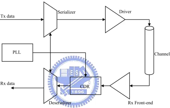
(11) Chapter1 Introduction. 1.1 Basic Serial Link Figure 1.1 shows a conventional serial link system. It comprises three fundamental components: a transmitter, a channel, and a receiver. The transmitter usually implements by a serializer and an output driver. The serializer converts parallel signal into serial. The serial data contains the timing information. The output driver is used to drive signal into the channel.. Tx data. Driver. Serializer. PLL. Channel. Rx data. CDR Deserializer. Rx Front-end. Figure 1.1: Conventional serial link transceiver architecture The second part of the serial link system is the channel. There are many types of channels for different applications. One of these channels is the copper wire. Unlike the optical fibers with larger bandwidth, the copper wires have limited bandwidth comparatively. But the advantage of the copper wire is its low cost. Therefore, the copper wire channel is popular in the high-speed systems. The receiver includes a front end amplifier, a clock and data recovery module(CDR)and a deserializer. In order to recover the signal, we need a receiver frond end amplifier to amplify the signal from channel. The CDR is used to resample the data by the recovered clock. Finally, the deserializer converts the high-speed and serial data into low speed and parallel data.. 2.
(12) Chapter1 Introduction. In additional, a serial link system also needs a phase lock loop(PLL) to as the clock source. The PLL provides high frequency clock to serializer and CDR. High-speed serial link systems are widely used in many applications such as communication within computers, data transmissions, and routes. Table 1.1 shows some popular communication standards.. Standard. Speed. USB2.0. 480Mbps. IEEE802.3. 1Gbps. Serial ATA. 1.5Gbps. IEEE1394b. 1.6Gbps ~ 3 .2Gbps. PCI Express. 2.5Gbps. Serial ATA II. 3Gbps. SONET OC-192. 9.95Gbps. Table 1.1 Standard of high-speed communication. 1.2 Motivation In high-speed serial link systems, the CDR is an important component. The data are transmitted through the channel, the signal is suppressed. We need a CDR to recover the data and clock. A good CDR recovers the data with low bit error rate (BER). That is, the main purpose of CDR recovers the data through channel with low bit error. Besides, the CDR design also reduces the jitters as much as possible. When a system operates at high speed, the spectrum is a concentrated pulse at certain frequency. It creates by Electro-Magnetic Interference(EMI). As a result, the spread spectrum technique is proposed[1]. The spread spectrum technique has a large frequency variation for traditional CDRs. In spread spectrum situation, conventional 3.
(13) Chapter1 Introduction. CDRs cannot tolerance the large frequency offsets in the specification. Therefore, we proposed a technique to compensate large frequency offset with low jitter.. 1.3 Thesis Organization This thesis comprises five chapters. Chapter 1 introduces the basis of serial link, the motivation and the thesis organization. In Chapter 2, we describe the background study. We will introduce the concept of spread spectrum. In addition, we also describe two basic types of CDR. Chapter 3 describes the consideration of the frequency compensation technique. In the proposed architecture, we derive the confidence counter size. Moreover, the optimal frequency compensation period is decided. Chapter 4 describes each block in detail. Behavior simulation, circuit simulation, and layout are shown in this chapter. Finally, we consider the test environment. Chapter 5 concludes this thesis and discussed the future development.. 4.
(14) Chapter2 Background Study. Chapter 2 Background Study. 2.1 Technique of CDR Basic method of CDR is shown in Figure 2.1. The noisy and asynchronous data is received from channel. We need a CDR to recover the clock and resample the data. The main function of CDR is to synchronize and reconstruct data, and reduce the accumulated jitter reduction. Decision Circuit D. Q. Recovered Data. Serial Data Input CDR Circuit Recovered Clock. Figure 2.1: Functionality of clock and data recovery circuit. 5.
(15) Chapter2 Background Study. Generally speaking, the CDR has two basic architectures. The PLL based CDR and the oversamoling based CDR use different concepts to architect a CDR. We discuss these two types of CDR in next paragraphs.. PLL based CDR Figure 2.2 shows the basic architecture of the PLL based CDR[2]. The difference between traditional PLL and PLL based CDR is the retiming circuit implemented by a D flip flop(DFF). The random data instead of reference clock is used as input. PLL based CDR comprises a phase frequency detector(PFD), a charge pump(CP), a low-pass filter(LPF), a voltage-controlled oscillator(VCO), and a retiming circuit. The PLL based CDR uses the PFD to detect the timing difference between the input data and the sampling clock. In order to adjust the VCO control voltage and filter out high frequency noise, the CP and LPF are designed. Finally, according to the control voltage, the VCO generates the sampling clock until the sampling clock and input data have no phase difference. Retiming Recovery Data. Data in PFD. Charge. LPF. Pump. VCO. Figure 2.2: PLL based CDR There is another similar type of CDR architecture, called DLL based CDR[2]. It. replaces the VCO by a voltage control delay line(VCDL). Unlink the VCO, the. VCDL adjusts the phase rather than the frequency.. 6.
(16) Chapter2 Background Study. Oversampling Based CDR Figure 2.3 shows the block diagram of the oversampling CDR[3]. The input data is sampled by a certain number of parallel samplers simultaneously. We also need a multi-phase clock generator to generate multi-phase clock. The outputs of the parallel samplers are stored. The bit boundary detection detects the data boundary by a majority voter. Finally, according to the bit boundary detection, we obtain the optimal clock to sample the data. Therefore, the data selector is implemented by a multiplexer to decide which sampled result is the recovered data.. Phase Detection. Parallel Samplers Data. Ref. Clock. DFF. DFF. DFF. DFF. Sample Storage. DFF. Multi-Phase Clock Generator. Data Selector Recovery Data. Bit Boundary Detection. Figure 2.3: Oversampling based CDR Figure 2.4 is an example of the oversampling technique. In this example, the data is sampled by three phases in every bit time. Every neighboring sampled results is exclusive-ored. to detect the data boundary. According to the accumulated. number of transitions, we decide the one of the maximum count to be the boundary. In this example, the maximum accumulated transition is six. We derive the transition edge is between phase 1 and phase 2. Finally, the best phase to sample is phase 3.[4]. 7.
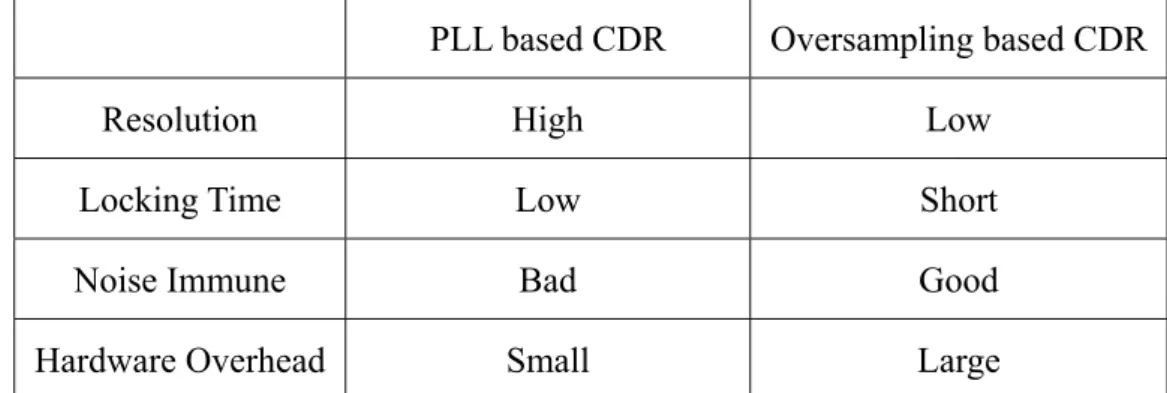
(17) Chapter2 Background Study. Input data Sampling Phases P1. P2 P3 P1. P2 P3 P1. P2 P3 P1. P2 P3 P1. P2 P3 P1. P2 P3. Sampled Value. 1 1 1. 0 0 0. 1 1 1. 0 0 0. 1 1 1. 0 0. 0. Indicate Transition. 1. Accumulate Transition. 0 0. 1 0 0. 1. 6. Transition Edge judgment. 0 0. 1. 0 0. 0. 1. 0 0. 1. 0. 0. P1-P2 P3. Phase Picked. Figure 2.4: Timing diagram of the oversampling. Comparison Two different types of CDR architecture are presented in the previous paragraphs. Table 2.1 lists the comparison between the PLL based CDRs and the oversampling based CDRs. Generally speaking, PLL based CDRs are an analog approach and oversampling based CDRs use a digital approach. Therefore, oversampling based CDRs are easy to be redesigned when the process technology is changed. It is one of the important advantages of the oversampling based CDRs. In Table 2.1, we compare some features of CDRs to understand the advantages and drawbacks in these two types of CDRs.. 8.
(18) Chapter2 Background Study. PLL based CDR. Oversampling based CDR. Resolution. High. Low. Locking Time. Low. Short. Noise Immune. Bad. Good. Hardware Overhead. Small. Large. Table 2.1: Comparison of PLL based CDR and oversampling CDR. 2.2 Basic of Spread Spectrum In order to reduce EMI, there are many techniques proposed. The spread spectrum is one of these techniques. The spread spectrum utilizes the frequency modulation to distribute the power. This technique is described in Figure 2.5[1]. Originally, the total power is concentrated at certain frequency. It induces large EMI. The spread spectrum reduces the maximum peak energy under the same total amount of energy. Only a small amount of variation in frequency is needed to obtain several decibels of energy reduction. In short, the spread spectrum is a popular, low cost, and efficient technique to reduce EMI. Non-Spread spectrum Spread spectrum Figure 2.5: Comparison of non-Spread spectrum and spread spectrum Figure 2.6 shows the Serial-ATA II requirement for 3Gbps transceiver systems [5]. The spread spectrum utilizes a 5000ppm down spreading and a 30~33kHz triangular profiles. According to this requirement, the lowest frequency is 2.985Gbps.. 9.
(19) Chapter2 Background Study. f 3Gbps 2.985Gbps (-5000ppm). 30~33kHz non-SSC SSC t. Figure 2.6: Spread spectrum requirement for Serial-ATA II Down spreading frequency modulation ensures the highest frequency is below the original frequency, 3Gbps. Serial-ATA specification defines a 30~33 kHz triangular modulation rate. In this requirement, the frequency varies with time.. 10.
(20) Chapter3 Frequency Compensation Technique. Chapter 3 Frequency Compensation Technique. Conventional CDRs, no matter PLL based or oversampling based, have less than 1000 ppm frequency tolerance. However, the Serial ATA requires a 5000ppm spread ratio. It induces very large jitter when input data has high frequency offset. Therefore, we propose a frequency compensation technique to enhance the tracking ability. The main contribution of this technique is the reduction the jitter at high frequency offset.. 3.1 Frequency Compensation Methodology In traditional CDR, it is not easy to track large frequency variation because the bandwidth is limited. In other words, small bandwidth induces smaller jitter, but the tracking ability is weak. On the contrary, if the CDR bandwidth is designed too large, it is good for frequency tolerance, but it obtains large jitter. In order to solve this trade off between bandwidth and jitter, we design another loop. Frequency compensation loop adds to a DLL based CDR[6]. The. 11.
(21) Chapter3 Frequency Compensation Technique. major purpose of the frequency compensation loop is to increase the CDR bandwidth. Only when the bandwidth is extended, the frequency tolerance is increased. The methodology of frequency compensation is shown in Figure 3.1. In Serial ATA, the spreading is a triangular waveform with 33kHz modulation frequency. For the frequency changes, we detect the amount of frequency variation in a frequency compensation period. In this thesis, the frequency compensation period is Ts . In Figure 3.1, we detect the frequency increment in section A. Therefore, the frequency compensation loop provides the same amount of frequency to compensate this increment in section B and so on. According to this methodology, we compensate the frequency in every Ts . ∆f Compensated Frequency. 1/33k t. ∆f1. ¼*1/33k ∆f0. Ts. A. B. Ts. Ts. Figure 3.1: The methodology of frequency compensation. 3.2 The Proposed CDR Architecture Figure 3.2 shows the proposed CDR architecture with frequency compensation. This architecture can be separated into two parts. The first part is a phase locked loop. It comprises a phase detector, a confidence counter, a phase control ,and a. 12.
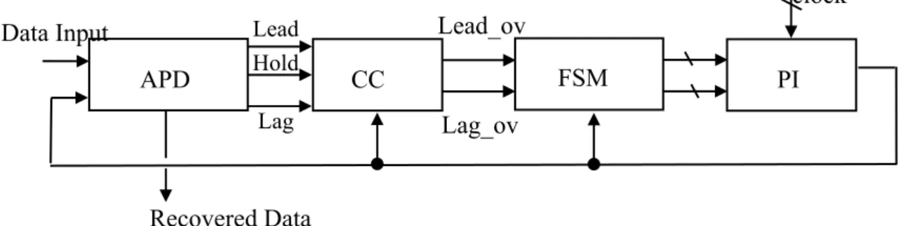
(22) Chapter3 Frequency Compensation Technique. phase selector. The second part is the frequency compensation loop. It comprises a pulse counter, a pulse accumulator, and a frequency error compensator (FEC). Besides, we design a lock detector to control the confidence counter size.. SSC_Data Input 3Gbps HRPD. Lock Detector Lead_p/ Lag_p Phase Control. Ts. Variable C.C.. 1.5G 8 phase Phase Selector. Lead_f/ Lag_f Recovery Clock. Pulse . Accum.. Pulse Counter. FEC. Ts. Figure 3.2: Proposed CDR architecture. Phase locked loop The phase locked loop can be simplified as shown in Figure 3.3. The phase detector (PD) is a bang-bang phase detector. The transfer curve of bang-bang phase detector is shown in Figure 3.4[7]. The PD can detect the relationship between input data and recovered clock. The PD output “LEAD” means the input data phase appears earlier than recovered clock and vice versa. clock Data Input APD. Lead Hold Lag. Lead_ov FSM. CC Lag_ov. Recovered Data Figure 3.3: Simplified phase locked loop architecture. 13. PI.
(23) Chapter3 Frequency Compensation Technique. PD out Lead ∆φ Lag. Figure 3.4: Transfer curve of bang-bang phase detector The Confidence Counter(CC) is similar to a loop filter functionally. The confidence counter size decides the equivalent bandwidth. In this thesis, the confidence counter size is N . If the number of accumulated input signal (Lead/Lag/Hold) exceeds N , the confidence counter have an output Lead_ov or Lag_ov. Lead_ov and Lag_ov are the inputs of the phase control. The coarse tune controls the choice of two neighboring phases from external clock. The fine tune interpolate phase more precisely. The phase control is designed with coarse tune and fine tune. Finally, the phase selector adjusts the phase to track the input data phase. In order to have more precise phase resolution, we use the interpolation technique in the phase selector. The advantage of high resolution is the jitter suppression. In other words, when this system is lock and stable, the recovered clock is lock between two phases. The higher the phase resolution, the smaller the jitter is induced. This architecture is implemented in digital. It is another advantage of this architecture.. Frequency Compensation loop The frequency compensation loop comprises three components. Figure 3.5 shows the block diagram of the frequency compensation loop.. 14.
(24) Chapter3 Frequency Compensation Technique. From Variable sized C.C. Pulse Counter. Pulse Accum.. Freq. Error Comp.. P0. Ts. P0. To Phase Control (FSM). Figure: 3.5 Frequency compensation loop The first one is the pulse counter. The pulse counter counts the number of pulse difference between lead pulses and lag pulses. This value means the frequency offset in a specific time. This specific time is the rate to update the number of compensated pulses. We denote the frequency compensation period Ts in this thesis. The pulse accumulator accumulates the pulses in every Ts . The final component of the frequency compensation loop is FEC. FEC can generate the same number of the pulses as the number in the pulses accumulation. And the pulse is generated as uniformly as possible. Finally, these pulses are used as the input of the phase control to adjust the phase in the phase selector. Every pulse adjusts the recovered clock one resolution.. 3.3 Confidence Counter Analysis The first key point in this design is to decide N . Intuitively, a smaller N produces an output quickly. That is, a smaller N represents a larger equivalent bandwidth. In the phase locked loop, we derive closed loop transfer function by the following steps: 1.Calculate the equivalent bandwidth for N of 6: Consider the random walk theory[8], we can calculate the expected value by the probability. The diagram is shown in Figure 3.6 15.
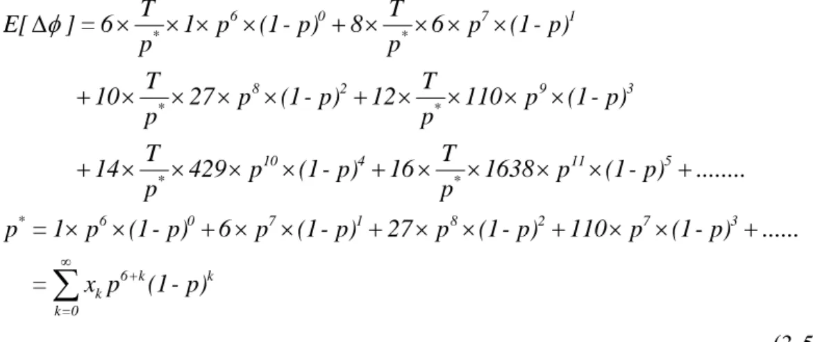
(25) Chapter3 Frequency Compensation Technique. P00 s0. •. P45. P34. s5. s4. s3 P43. P56. P67 s6. s7. P89 s8. P87. P76. P65. P54. P78. s9. •. s12 P12 12. P98. Figure 3.6: Modify the confidence counter as a Markov chain[9] In Figure 3.6, the probability from state “ i ” to “ j ” is Pij = Pr(X 1 = j X 0 = i) .. (3-1). Define the probability of going from state “ i ” to state “ j ” in n time steps as Pijn = Pr(X 1 = j X 0 = i) .. (3-2). Using the first passage time, we modify (3-2) as. Pij(n) = ∑ Pik × Pkj(n-1). for i =6, j =12 must n =6,8,10….. (3-3). k≠ j. Now we use (3-3) to calculate the combinations of Pijn for different n . Therefore, we establish the matrix (3-4). P0n,12 P1n,12 P2n,12 P3n,12 P4n,12 P5n,12 P6n,12 P7n,12 P8n,12 P9n,12 P10n ,12 P11n,12 N=1 ⎡ 0. 0. 0. 0. 0. 0. 0. 0. 0. 0. 0. N=2. 0 0. 0 0. 0 0. 0 0. 0 0. 0 0. 0 0. 0 0. 0 1. 1 0. 0 0 0. 0 0 0. 0 0 0. 0 0 0. 0 0 0. 0 0 1. 0 1 0. 1 0 4. 0 3 0. 2 0 5. 0. 0. 0. 0. 1. 0. 5. 0. 9. 0. 0. 0. 0. 1. 0. 6. 0. 14. 0. 14. ⎢0 ⎢ N=3 ⎢ 0 ⎢ N=4 0 ⎢ N=5 ⎢ 0 ⎢ N=6 ⎢ 0 N=7 ⎢ 0 ⎢ N=8 ⎣ ⎢0. 1⎤ 0 ⎥⎥ 1⎥ ⎥ 0⎥ 2⎥ ⎥ 0⎥ 5⎥ ⎥ 0 ⎦⎥ (3-4). Second, we use the expected value of conditional probability to calculate the time that confidence counter output occurs.. 16.
(26) Chapter3 Frequency Compensation Technique. T T × 1 × p6 × (1- p)0 + 8 × * × 6 × p7 × (1- p)1 * p p T T + 10 × * × 27 × p 8 × (1- p)2 + 12 × * × 110 × p 9 × (1- p)3 p p T T + 14 × * × 429 × p10 × (1- p)4 + 16 × * × 1638 × p 11 × (1- p)5 + ........ p p. E[ Δφ ] = 6 ×. p* = 1 × p6 × (1- p)0 + 6 × p7 × (1- p)1 + 27 × p 8 × (1- p)2 + 110 × p7 × (1- p)3 + ...... ∞. = ∑ xk p6+k (1- p)k k=0. (3-5) In (3-5), p means the probability of lead. Therefore, we assume the input jitter is a Gaussian distribution in Figure 3.7. The probability of lead can be calculated as ∞. p = ∫ f(x)dx Δφ. = Q(. Δφ. σ. .. (3-6). ) f(x). x Lag. Lead. ∆φ. Figure 3.7: Gaussian distribution profile In (3-5), parameter ζ is represented the number was circuited by dot square in (3-4). We can extend the matrix to a general from by following derive.. ζ0 = 1 6. ζ 1 = 1+1+1+1+1+1= ∑ 1 j=1. 17.
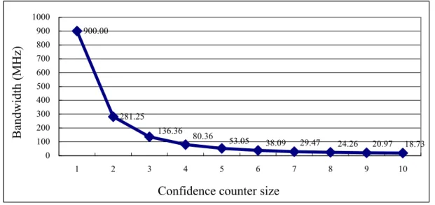
(27) Chapter3 Frequency Compensation Technique 6. i+1. ζ 2 = 27 = 2+3+4 + 5+6 +7 = ∑ ( ∑ 1) i=1. j=1. 6. ζ 3 = 110 +5+9 +14 + 20 + 27 + 35 = ∑ r=1. r+1. i+1. i=1. j=1. ∑ ( ∑ 1). The general form of ζ is 6. k -2. ji+1 +1 j1 +1. jk-1 =1. i=1. ji =1 j0 =1. ∑ ∏ ∑ ∑1. ζk =. .. (3-7). Rewrite (3-5): (6 + 2n) × ζ n × p6+n (1- p)n ×T p* n=0 ∞. E[ Δφ ] = ∑ ∞. = ∑ (6 + 2n) ×. ζn. n=0. p*. × [Q(. Δφ. )]. σ. 6+n. [1- Q(. Δφ. σ. .. (3-8). )] × T n. (3-8) means the excepted value for the confidence counter to obtain an output. We can derive the equivalent bandwidth from (3-8).. ωC_C =. 2.. 1 E[ Δφ ]. (3-9). Rewrite the equivalent bandwidth in a general form:. (3-8) can replace the confidence counter size 6 by N . We obtain the equivalent bandwidth of confidence counter as ∞. ωc_c = 2π × { ∑ (N + 2k) × k=0. ζk *. P. × [Q(. Δφ. σ. )] N + k [1- Q(. Δφ. σ. )] k × T}-1 .. (3-10). According to (3-10), the relationship between confidence counter size N and equivalent bandwidth is plotted in Figure 3.8.. 18.
(28) Chapter3 Frequency Compensation Technique. 1000. Bandwidth (MHz). 900. 900.00. 800 700 600 500 400 300. 281.25. 200. 136.36. 80.36. 100. 53.05. 29.47. 38.09. 24.26. 20.97. 18.73. 0 1. 2. 3. 4. 5. 6. 7. 8. 9. 10. Confidence counter size Figure 3.8: The relationship between N and equivalent bandwidth. From Figure 3.8, we achieve the result that the larger the confidence counter size, the smaller the equivalent bandwidth.. 3.. Phase selector transfer function:. Besides the confidence counter, there is another component in phase locked loop. The phase selector adjusts the phase when the control digital code changes. We modify the relationship between digital code and output phase in Figure 3.9. Therefore, we linearizes the relationship curve. Eventually, the transfer function of phase selector K PI is represented in (3-20): ∆φ 2π. (2π/16)*2 (2π/16)*1 12. 16. Figure 3.9: Phase selector transfer curve. 19. Digital Code.
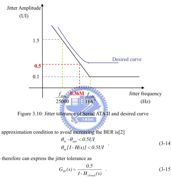
(29) Chapter3 Frequency Compensation Technique. K PI =. 2p 2p = 16 L. (3-11). where L is the interpolation steps. 4.. Phase locked loop transfer function:. From (3-10) and (3-11), the phase locked loop transfer function is derived under these assumptions: Assumption 1: The input jitter is a Gaussian distribution Assumption 2: The phase selector transfer curve is linearized Assumption 3: Only consider the input jitter in ±3σ Assumption 4: Δφ is half the resolution. The phase locked loop closed transfer function can be represented in (3-12) by these assumptions.. KI. H closed (s)=. (K I +1)+. s. (3-12). ωc_c. R ζ Where ωc_c = 2π × { ∑ (N + 2k) × k* × [Q( 2 )] N + k [1- Q( Ji P k=0 6 ∞. R 2 )] k × T}-1 .(3 -13) Ji 6. In (3-12) and (3-13), the phase locked loop transfer function depends on four parameters. N is the confidence counter size.. R is the phase resolution. J i is the peak to peak input jitter.. T is the clock period. Besides, P* and ζ k are shown in (3-5) and (3-7). Jitter tolerance is an important specification for CDRs. Jitter tolerance is defined as input jitter a receiver must tolerance without violating system’s BER specification. Jitter tolerance specification of Serial ATA II is shown in Figure 20.
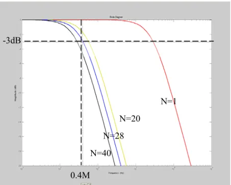
(30) Chapter3 Frequency Compensation Technique. 3.11[5]. The available region is upper the jitter tolerance mask. As a result, we design our desire curve as the dotted line. In Figure 3.10, if we deign the phase locked loop bandwidth at 0.4MHz, it suits for the jitter tolerance.. Jitter Amplitude (UI). 1.5 Desired curve 0.5. 0.1 f data 0.36M f data 25000 1667. Jitter frequency (Hz). Figure 3.10: Jitter tolerance of Serial ATA II and desired curve An approximation condition to avoid increasing the BER is[2] θin - θ out < 0.5UI . θin [1- H(s)] < 0.5UI We therefore can express the jitter tolerance as 0.5 . GJT (s)= 1 - H closed (s). (3-14). (3-15). The relation between jitter tolerance and phase locked loop closed transfer function is shown in Figure 3.11. According to the phase locked loop closed transfer function (3-12), we can calculate the equivalent bandwidth by different N . The result is shown in Figure 3.11. When N is 28, the equivalent bandwidth is 0.4MHz. Eventually, in order to be easy for circuit design, we choose N =32 as the confidence counter size.. 21.
(31) Chapter3 Frequency Compensation Technique. -3dB. N=1 N=20 N=28 N=40 0.4M Figure 3.11: The equivalent frequency response of C.C. by different size In short, in our design the confidence counter size is 32. As the result, the equivalent bandwidth satisfies the Serial ATA II jitter tolerance requirement.. 3.4. Frequency Compensation Period Determination. The second key point in our design is to determine the frequency compensated period. In Figure 3.1, the spread spectrum is a triangular profile. Therefore, the amount of frequency increment is fixed. In Figure 3.12, we calculate the slope of the frequency offset.. 22.
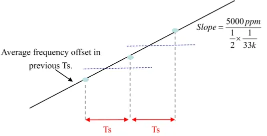
(32) Chapter3 Frequency Compensation Technique. Slope = Average frequency offset in previous Ts.. Ts. 5000 ppm 1 1 × 2 33k. Ts. Figure 3.12: Relationship between Ts and frequency offset According to the Serial ATA II specification[5], the modulation frequency is 33kHz, and spread ratio is 5000ppm. As the result, we can derive the equation: Δf = slope × Ts = 330 × Ts . (3-16) where Δf means the frequency offset.. The longer the Ts is, the larger the frequency offset will be. But the longer the Ts , the more precious equivalent frequency offset be calculated. It is a trade off between the Ts and the frequency offset. In this design, we design the maximum error tolerance is two resolutions in Ts . We represent it as 1 32 = Δf Ts × f clk 2×. .. (3-17). ⇒ 41.68p = Δf × Ts. In this design, the number of resolution steps is 32. And Ts multiplies f clk means the number of clocks in Ts . Finally, (3-17) means at the maximum frequency offset, the maximum compensated error is 2 times resolution. From (3-16) and (3-17), we can find the optimal Ts and the equivalent frequency offset. Figure 3.13 shows the results from these two equations.. 23.
(33) Chapter3 Frequency Compensation Technique. Δf(ppm ). 117.15 112.53. 0.355u 0.341u (512clock) (533clock). Ts. Figure 3.13: Determination of Ts The optimal Ts is 0.355us. In order to simplified the circuit design , we choose the Ts =0.314us. Ts is 0.341us represents that a Ts is 512-clock cycles. Therefore, in every Ts , the frequency offset is 112.53ppm.. 24.
(34) Chapter4 Implementation of Clock and Data Recovery. Chapter 4 Implementation of Clock and Data Recovery. In this chapter, we describe the detail of the circuit implementation. The proposed system block diagram is shown in Figure 4.1. Therefore, we have behavior simulation to verify this design functionally. Besides, the circuit level simulation predicts the performance. Finally, the layout is shown, and the test environment setup is proposed.. SSC_Data Input 3Gbps HRPD. Lock Detector Variable C.C.. Lead_p/ Lag_p Phase Control. Ts. 1.5G 8 phase Phase Selector. Lead_f/ Lag_f Recovery Clock. Pulse Counter. Pulse . Accum.. FEC. Ts Figure 4.1: Proposed system block diagram. 25.
(35) Chapter4 Implementation of Clock and Data Recovery. 4.1 Building Blocks There are eight blocks in proposed CDR as Figure 4.1. We describe these blocks respectively.. Half Rate Phase Detector The half rate phase detector (HRPD) detects two bit boundary is lead, lag or hold in a clock cycle. HRPD needs 4-phase clock source to sample the input bit stream. The considerations is shown in Figure 4.2. Input data 3Gbps P0(1.5GHz) P1 P2 P3 Figure 4.2: HRPD timing diagram In Figure 4.2, P0 and P2 detect the boundary of the input data, and P1 and P3 can sample the data. The circuit implementation is shown is Figure 4.3.[10]. By this operation, there are two answers of lead, lag ,or hold in every clock cycle. It is the reason that the architecture is called half rate. The output of HRPD has 4 bits. Lead 1 and Lag 1 represent the relation between the input data and recovered clock in the first bit boundary. Lead 2 and Lag 2 are for the second bit boundary. For example, if (Lead1,Lag1,Lead2,Lag2)=1000, it means that the first boundary leads the clock and the second boundary has no transition.. 26.
(36) Chapter4 Implementation of Clock and Data Recovery. DFF Data in. DFF. DFF Lead1. P0 DFF. DFF Lag1. P1 DFF P2. Lag2. DFF Lead2. DFF. DFF. P3 P0 Figure 4.3: Half Rate Phase Detector Therefore, we need an encoder to transform the output of the HRPD output into 2’s complement format. Table 4.1 is the truth table of this transformation. If the Lead1 and Lead2 are 1s, we transform into the 010(+2). On the contrary, if the Lag1 and Lag2 are 1s, we transform into the 110(-2). The positive number means lead and the negative number means lag. Finally, the boolean function of the encoder is (4-1). And, the encoder is implemented by static CMOS logic.. A2 = S 3S 2( S1 + S 0) + S 0 S1( S 3 + S 2) A1 = S 3S 2( S1 + S 0) + S 0 S1( S 3 + S 2) + S 3S 2 S1S 0 A0 = S 3 ⊕ S 2 ⊕ S1 ⊕ S 0. 27. (4-1).
(37) Chapter4 Implementation of Clock and Data Recovery. PD Output S3 S2 S1 (Lead1) (Lead2) (Lag1) 0 0 0. Encode S0 (Lag2) 0. A2 (sign) 0. A1. A0. 0. 0. 0. 0. 0. 1. 1. 1. 1. 0. 0. 1. 0. 1. 1. 1. 0. 0. 1. 1. 1. 1. 0. 0. 1. 0. 0. 0. 0. 1. 0. 1. 0. 1. 0. 0. 0. 0. 1. 1. 0. 0. 0. 0. 0. 1. 1. 1. 1. 1. 1. 1. 0. 0. 0. 0. 0. 1. 1. 0. 0. 1. 0. 0. 0. 1. 0. 1. 0. 0. 0. 0. 1. 0. 1. 1. 1. 1. 1. 1. 1. 0. 0. 0. 1. 0. 1. 1. 0. 1. 0. 0. 1. 1. 1. 1. 0. 0. 0. 1. 1. 1. 1. 1. 0. 0. 0. Table 4.1: Encoder truth table. Variable-Sized Confidence Counter In Chapter 3, we have introduced the function of the confidence counter. According to the analysis in Chapter 3, the confidence counter size decides the equivalent bandwidth. A smaller N is equivalent to the larger bandwidth and better tracking ability. In order to compensate initial frequency offset, we choose N to be 2 initially. Then, N is increased to 8. Finally, N is fixed at the desired value 32. By adjusting the size of the confidence counter, we change the equivalent bandwidth. Therefore, it is called variable-sized confidence counter. The circuit of the variable-size confidence counter is shown in Figure 4.4.. 28.
(38) Chapter4 Implementation of Clock and Data Recovery. From Lock L[2:0] Detector. A[2:0] B[5:0]. 6-bit Adder. DFF SO[5:0] Register ×6 rst. SO5 SO3 SO1. 100 010. Lag. Q/Qb. 001. Lead. P0. Reset 6. Figure 4.4: Variable-sized confidence counter. In Figure 4.4, a 6-bit adder is designed. SO[5:0] are output bits of the 6-bit adder. For example, when N is 2, we detect that when SO1 changes the value. For N of 2, 8, and 32, we detect SO1, SO3, and SO5. In Table 4.2, the boldface. represents that bit value being changed. Simultaneously, the variable sized confidence counter generates a output pulse. Moreover, if the input of the variable size confidence counter is lead, it represents positive value. When the accumulated value is +2, there is a lead output pulse. On the contrary, when the accumulated value is -3, another lag output pulse is generated. It is an asymmetry decision.. Decimal. SO5. SO4. SO3. SO2. SO1. SO0. +2. 0. 0. 0. 0. 1. 0. +8. 0. 0. 1. 0. 0. 0. +32. 1. 0. 0. 0. 0. 0. -2. 1. 1. 1. 1. 1. 0. -3. 1. 1. 1. 1. 0. 1. -8. 1. 1. 1. 0. 0. 0. -9. 1. 1. 0. 1. 1. 1. -32. 1. 0. 0. 0. 0. 0. -33. 0. 1. 1. 1. 1. 1. 29.
(39) Chapter4 Implementation of Clock and Data Recovery. Table 4.2: 6-bit adder output in variable sized confidence counter (partial) The adjustment of confidence counter number is decided by the lock detector. We will introduce the behavior and circuit of the lock detector later. Consider a clock frequency of 1.5GHz, it means that confidence counter must achieve its function in 666.6666ps. In Figure 4.4, we design a 6-bit adder with delay as small as possible. As the result, the 6-bit adder is shown in Figure 4.5. It is a carry-look-ahead(CLA) structure[11]. In order to reduce the propagation delay, we implement these gates by the pseudo NMOS logic rather than the static logic. From the simulation, the critical path in this 6-bit adder is 460ps.. A0 B0. P0. S0. G0 (C1) A1 B1. S1. P1 G1. C2. C2=P1G0. S2 A2 B2. P2 G2. A2 B3. C3=P2P1G0+P2G1+G. S3. P3 G3. A2 B4. B5. C4=P3C3. C4 S4. P4 G4. A2. C3. C5=P4P3C3+P4G3+G. C5 S5. P5 Figure 4.5: The structure of 6-bit adder. 30.
(40) Chapter4 Implementation of Clock and Data Recovery. Phase Control The phase control has two input source. One is the phase locked loop control and another control is from frequency compensation loop. Functionally, the phase control is a finite state machine to control the adjustment of phase. The phase control is separated into two parts. The first part is the fine tune. We use four bit to control the interpolation. Figure 4.6 is the fine tune circuit.. Lead_ft Lag_ft Hold_ft D0. D1. D2. D3. Clk. Figure 4.6: Fine tune circuit Only when the input is Lead_ft or Lag_ft, the state of D3~D0 change. The fine tune state diagram is shown in Figure 4.7. Every state represents a resolution in phase difference. The four bits control the total amount of the interpolation.. Lead. Podd. Peven 0000. 0001. 0011. 0111. 1111. Peven+2 1110. 1100. 1000. 0000. Lag Figure 4.7: State diagram of fine tune (partial) The second part is the coarse tune. Because we have a 8-phase PLL to generate. 31.
(41) Chapter4 Implementation of Clock and Data Recovery. the clock, we deign the coarse tune as Figure 4.8.. Lead_ct Lag_ct Hold_ct. CA1. CB1. CA2. CB2. CA3. CB3. CA4. CB4. Clk DFF reset to 1 Figure 4.8: Coarse tune circuit We must choose two neighboring phases to do the interpolation. Initially, the first two D flip-flop (DFF) are designed in a reset-to-1 format. Therefore, CA1 and CB1 are 1 and others are 0. As the result, phase 0 and phase 1 are chosen to interpolate. The state diagram is shown in Figure 4.9. CA[3:0] Selected Phase CB[4:0]. 0001 P0/P1 0001 Lead. 0010 P2/P1 0001. 0010 P2/P3 0010. Lag 0001 P0/P7 1000. 0100 P4/P3 0010. 1000 P6/P7 1000. 1000 P6/P5 0100. 0100 P4/P5 0100. Figure 4.9: State diagram of coarse tune. The coarse state adjustment control bit is called Lead_ct, Lag_ct, and Hold_ct. The coarse tune control bits are implemented in Figure 4.10.. 32.
(42) Chapter4 Implementation of Clock and Data Recovery. Lead_ft d4p. Lead_ct. DFF. d4. Hold_ct. d1. DFF. Lag_ct. d1p cks. Lag_ft. Figure 4.10: Control tune control bit. The coarse tune changes the state only when fine tune state is 1111 or 0000 and Lead_ft or Lag_ft are input simultaneously. Then, we adjust the coarse tune state. In other words, we change the source clock to do interpolation.. Phase Selector The phase selector has 8 coarse tune control bits, 4 fine tune control bits, and 8-phase clock source input. The output is a 4-phase clock to HRPD. It is shown in Figure 4.11. 1.5G 8 phase. Coarse tune 8. Fine tune. Phase Selector. 4. 4. To HRPD. Figure 4.11: Phase selector input and output pins. Circuit structure of the phase selector is shown in Figure 4.12. CA[3:0] and CB[3:0] are the 8 control bits of the coarse tune. We use these coarse tune bit to decide which two neighboring phase are chosen. Then, the phase interpolation technique is applied. We design 4 parallel tri-state inverters to have the same input. 33.
(43) Chapter4 Implementation of Clock and Data Recovery. phase. Another 4 parallel tri-state inverters also have the same width input. Therefore, the output phase is interpolated according to these tri-state inverters is on or off respectively. In our design, we need 4 phase outputs. Two sets of the same architecture are designed. Both of these architectures are differential. Because our PLL generates 8-phase 1.5GHz clock source, the neighboring phases have 83.3333ps phase difference. The architecture of the phase selector is shown in Figure 4.12. Two neighboring phases are interpolated to 4 phases. Therefore, this architecture has the number of 32 resolution steps. In other words, each fine tune adjusts 20.83ps phase in ideal case. This architecture utilities tri-state inverters to implement interpolation digitally. Figure 4.13 shows the simulation of the phase interpolation and Table 4.3 is the simulation results and errors. In Table 4.3, the simulation results show that we have 1.2% phase error by the interpolation technique.. P0 P2 P4 P6. X0 X1 X2 X3 CA[3:0]. d[3:0]. PO0/PO2. P1 P3 P5 P7 CB[3:0] P2 P4 P6 P0. X0 X1 X2 X3 CA[3:0]. d[3:0]. PO1/PO3. P3 P5 P7 P1 CB[3:0] Figure 4.12: Phase selector architecture 34.
(44) Chapter4 Implementation of Clock and Data Recovery. Figure 4.13: Simulation of phase selector Ideal section period=20.83ps. s1. s2. s3. s4. Section Period (ps). 20.87. 20.86. 20.57. 21.01. Error(%). 0.19. 0.14. -1.2. 0.86. Table 4.3: Phase selector phase period and phase error. Pulse Counter The pulse counter counts the number of difference between Lead_p and Lag_p from variable size confidence counter in every Ts . In our design, the maximum frequency offset is 5000ppm. 5000ppm means every 1000 clock cycles have 5 unit interval(UI) phase error. As a result, when Ts is 512 clocks, it has 2.5 UI phase error in a Ts . We need 80 phase adjustments to compensate 2.5UI phase error in 1/32 resolution. Therefore, we design a 8-bit up/down counter as the pulse counter. The 8-bit up/down counter is shown in Figure 4.14.. 35.
(45) Chapter4 Implementation of Clock and Data Recovery. Lag_p Lead_p TFF S0. TFF S1. TFF S2. TFF S3. TFF S4. TFF S5. TFF S6. TFF S7. Figure 4.14: Pulse counter To reduce propagation delay, we use pseudo NMOS logic to design the up/down counter. The number of the pulse counter means the equivalent frequency offset in a Ts .. Pulse Accumulator The pulse accumulator adds the value which is counted in the pulse counter. The accumulated value means the equivalent frequency offset. That is, we track the frequency variation along with the accumulated value changes in the pulse accumulator. We call the technique is incremental because the accumulated value in the pulse accumulator is changed gradually. Because the accumulated value is updated in every Ts , the pulse accumulator is implemented by a traditional 8-bit CLA adder.. Frequency Error Compensator FEC is the heart of the frequency compensation loop. According to the accumulated value in the pulse accumulator, FEC generates the same numbers of pulses in Ts . Because the frequency variation is linear in spread spectrum, FEC must generate the pulse as uniformly as possible. These pulses are the control bits to adjust the phase. Using these pulses, we compensate the frequency offset. The structure of FEC is shown in Figure 4.15. We utilize a ripple counter[12], a 7-bit counter, and some logic gates to generate C0~C6. The ripple counter is serial four DFFs. The ripple counter converts the clock from 1.5GHz to 375MHz. In other words, the signal Clk_r have a transition in 4 clock cycles. The 7-bit counter is 36.
(46) Chapter4 Implementation of Clock and Data Recovery. triggered by Clk_r. After the 7 output bits of counter and Clk_r are operated in some logic gates, we obtain C0~C6. C0 generates 128 pulses in a Ts . And C1, C2, C3, C4, C5, and C6 generate 64, 32, 16, 8, 4, 2, and 1 pulses respectively. Besides, the 8-bit accumulator stores the number of pulses which must generate in FEC. SF7 in 8-bit accumulator is the sign bit. We use SF7 to control 7 multiplexers (MUXs). These MUXs decide that the positive value or the negative value is applied to FEC. Eventually, we determine C0~C6 which signals are chosen by the valued in accumulator. Lead_f or Lag_f generates the same number of pulses in a Ts .. C6 SF6. C5 2-1 MUX Groups. 8-bit Accum. Uniform pulse gen. logic MSB. C4 7 bit Counter. C3 C2 C1 C0. SF0 SF7. LSB Clk_r. Leadb_f. Ripple Counter P0. Lagb_f Figure 4.15: Frequency Error Compensator. For example, when the accumulated value is 20, the binary number SF[7:0] is 00010100. Figure 4.16 shows the timing diagram of this example. Because the sign bit SF7 is 0, Lead_f has output pulses. According to SF4 and SF2 are 1, we derive C2 and C4 are chosen to generate the output. C2 generates 16 pulses in a Ts and C4 generates 4 pulses. Therefore, Lead_f have 20 pulses in the Ts to compensate the 37.
(47) Chapter4 Implementation of Clock and Data Recovery. frequency offset. P0 (1.5GHz) Clk_r Clk_r C0 C1 C2 C3 C4 C5 C6 Lead_f Lag_f Figure 4.16: Timing diagram of FEC. Lock Detector The lock detector controls the size of the variable sized confidence counter. The confidence counter size decides the bandwidth. Therefore, we adjust the confidence counter size to enhance the tracking ability. Now, the lock detector is a component to judge when to adjust the confidence counter size. It is called lock in the system with frequency variation when the number of the confidence counter output Lead_p and Lag_p have small difference. For this reason, we assume the input jitter is 0.3 UI and Gaussian distribution. Then, we consider the input jitter in ±3σ . If the difference of Lead_p and Lag_p is smaller than a resolution, it is locked. In our design, a resolution is 20.83ps and 1 σ is 33.33ps. We derive the locked region as Lead _ p : Lag _ p = Q(. 10.41 10.41 ) : 1- Q( )= 37.5% : 62.5% 33.33 33.33. (4-2). and vice versa. In short, if the difference between Lead_p and Lag_p is smaller than 62.5%-37.5%=25%, we decide the system is locked. This concept is shown in Figure 4.17. After the lock detector is locked, the confidence counter size increases and the equivalent bandwidth is smaller.. 38.
(48) Chapter4 Implementation of Clock and Data Recovery. f(x). Lead_p(37.5%). Lag_p(62.5%). -3σ. -3σ. x. 1 Resolution Figure 4.17: The concept of the lock detector. The implementation of the lock detector is shown in Figure 4.18. We detect the output of the pulse counter SS[7:0] to be the input of the lock detector. The pulse counter calculates the difference of Lead_p and Lag_p in every Ts . Initially, the confidence counter size N is 2. Because the ratio between Lead_p and Lag_p is 96 160 : = 37.5% : 62.5% 256 256. (4-3). we judge the system is locked. That is, when the difference of the number of pulses is smaller than 64 in 512 clock cycles, the system is locked.. Therefore, SS6 and SS5 are detected that whether the value is changed or not. If the one of them is changed, it means the difference is lager than 64. The system is unlocked. On the contrary, if SS5 and SS6 maintains their value in a Ts , it represents the system is locked. We adjust N to 8. When N is 8, we detect SS4 and SS3 to judge the system is locked or not. Finally, N is adjusted to 32. In Chapter 3, we analyze that N =32 is the desired value.. 39.
(49) Chapter4 Implementation of Clock and Data Recovery. L[2:0]: SS3 SS4 SS5 SS6. 0. 001 010 100 N=2 N=8 N=32. 10. 1 0. 01. 1. L[1:0]. SS. rst 1 L0. L1. L2. Tsd Figure 4.18: Lock detector. 4.2 Simulation Results Behavior Simulation We use SIMULINK to analyze the proposed system behavior function. Especially, the frequency compensation loop and the concept of lock detector are verified by the behavior simulation. Figure 4.19 shows the behavior model of the proposed system. In order to experiment the function of the system, we generate the data with spread spectrum as the system input.. Figure 4.19: Behavior Simulation 40.
(50) Chapter4 Implementation of Clock and Data Recovery. Figure 4.20 shows the tracking ability of system when the input without frequency offset initially. The number of compensation pulses are incremental along with the frequency varies. Figure 4.21 shows the result of frequency compensation when input with 5000ppm frequency offset initially. In Figure 4.21, the system detects this large frequency offset in the first Ts . Therefore, the number of compensation pulses increases to 80. 80 compensation pulses are equivalent to 5000ppm frequency offset in the previous discussion. Then the system has eliminated the initial frequency offset. The system returns to the incremental frequency compensation.. Ts. Acc.# of pulse Count # of pulse in previous Ts Input Frequency Figure 4.20: Behavior Simulation when input without offset initially. Ts. Acc.# of pulse Count # of pulse in previous Ts Input Frequency Figure 4.21: Behavior Simulation when input with 5000 ppm offset initially. 41.
(51) Chapter4 Implementation of Clock and Data Recovery. Circuit Level Simulation The circuit level simulation uses Hspice to simulate. We also use 3Gb/s random data without initial frequency offset as the system input. The simulation results are shown in Figure 4.22. Because the input spread spectrum is down spreading, the compensation pulses are Lead_f. And the number of pulses varies according to frequency variation. Figure 4.23 shows the circuit simulation results when input data with 5000ppm frequency offset. It is similar to the behavior simulation that in first Ts the system generates Lead_f pulses to compensate frequency offset. Then, the compensation pulses are incremental to compensate spread spectrum frequency variation.. Ts. Lead_f. Lag_f. 35. 38. 48. 41. 45. Figure 4.22: Circuit simulation when input without offset initially. 42. 42.
(52) Chapter4 Implementation of Clock and Data Recovery. Ts. Lead_f. Lag f. 54. 50. 11. 46. 14. 17. Figure 4.23: Circuit simulation when input with 5000ppm offset initially. Moreover, we also simulate the proposed CDR when the input without frequency variation. In the CDR the recovered clock is locked in two neighboring phases. The recovered data is shown in Figure 4.24. The peak-to-peak jitter is 35ps.. 35ps. Figure 4.24: The recovered data when input without frequency variation. Comparison Figure 4.25 and Figure 4.26 show the comparison with ideal spread spectrum, behavior simulation results, and circuit level simulation results when input data 43.
(53) Chapter4 Implementation of Clock and Data Recovery. without frequency offset and with 5000ppm frequency offset. In Figure 4.26, when input with 5000ppm frequency offset initially, the number of compensation pulses increases to 120. It is too large to compensate frequency offset. Fortunately, the system corrects in next Ts . In short, both of these two cases operate in the desired function. That is, the frequency compensation loop has shown its advantages to recover spread spectrum frequency offset. 90 80 70. # of pulses. 60 50 40 30 20 10 0 -10 0. 10. 20. 30. 40. 50. 60. 70. 80. 90. Ts SS Triangular Profile. Behavior Simulation. Circuit Simulation. Figure 4.25: Comparison when input without offset initially. 140 120. # of pulses. 100 80 60 40 20 0 0. 10. 20. 30. 40. 50. 60. 70. 80. Ts SS Triangular Profile. Behavior Simulation. Circuit Simulation. Figure 4.26: Comparison when input with 5000ppm offset initially. 44. 90.
(54) Chapter4 Implementation of Clock and Data Recovery. 4.3 Tape Out and Chip Summary The proposed CDR is implemented by National Chip Implement Center (CIC) with T18-96E. The chip area is 920um*1040um as shown in Figure 4.27. In this chip, we have not only the proposed CDR but also a 1.5GHz 8-phase PLL[13]. The PLL is served as a clock source and provide the 8-phases clock to the phase selector in the proposed CDR. In the chip, we use 3 power pads. The first one provides power for the CDR. The second one is PLL’s voltage source. And the third power provides the power to other test circuit and the output drivers. We use 28 pads totally. This chip is implemented by TSMC 0.18um 1P6M technology. Ref clk. vd2. gd2. vcpb. Div out. Clk. gd33. Ctrlb Clkb. SSCb_in. PLL. SSC_in. gd33. gd3. vd3. Re data. Re clkb. Re datab. Re clk. Core L1 gd1 Lag_p. Ts. gd32 Lead p. Rstb. vd1. Lag f. Figure 4.27: Chip layout. 45. Lead f.
(55) Chapter4 Implementation of Clock and Data Recovery. The chip summarized in Table 4.4. The total power is about 158mW. It includes the CDR core, the PLL, the test circuit, and the output drivers. The proposed CDR has 60.8mW power consumption and 390×400um2. Moreover we have a ±5000ppm frequency tolerance in the proposed CDR. Specification Technology. TSMC 0.18um 1P6M. Power Supply. 1.8V. Input Data. 3Gbps with Spread Spectrum. `Chip Size. 1040umx920um. Chip Power. ~158mW. Core Size. 390umx400um. Core Power. 60.8mW. PLL Size. 305umx315um. PLL Power. 30mW. Frequency Tolerance. ±5000ppm. Table 4.4: Chip Summary. 4.4 Test Environment Setup In order to verify the proposed CDR, we consider the measurement setup. In the chip, we have some components are designed for measurement. The test environment setup is shown in Figure 4.28. The blocks in Figure 4.28 are implemented in the chip. The 3Gb/s spread spectrum data is provided by Agilent N4903A and the Pseudo Random Bit Sequence (PRBS) circuit. The clock has two kinds of sources. One is the 1.5GHz 8-phases PLL. Another one utilities Agilent N4901B to provide differential 6GHz clock and divides the 6GHz clock to 1.5GHz 8-phase by the 8-phase clock generator. Therefore, we design the MUX to control which clock source is chosen. In the. 46.
(56) Chapter4 Implementation of Clock and Data Recovery. output measurement side, the output data is serialized by the 2-to-1 serializer. And the recovered data and recovered clock are driven by the output buffer. We measure the recovered data and clock by Agilent N4901B Serial BERT. Because we setup our polynomial function of PRBS in Agilent N4901B, the BER is measured. Besides, Lead_p, Lag_p, Lead_f, and Lag_f are measured by Agilent 86100B oscilloscope. The frequency tracking ability is shown according to the number of pulses in Lead_f and Lag_f in every Ts .. Agilent 81130A Function Generator. 93.75M Hz Clock. Agilent N4901B 13.5-Gbps Serial BERT. 8-phase Clock Generator. 1.5GHz 8-phase PLL. HP E3610A. 6 GHz Clock. DC Poser Supply. Clock Source Control. MUX PRBS Generator Agilent N4903A SSC Generator. CDR Core. Lead_p/ Lag_p. SER 2:1. Lead_f/ Lag_f. Agilent 86100B Wide-Bandwidth Oscilloscope. Re_data/ Re_datab. Output Buffer. Re_clk/ Re_clkb. Figure 4.28: Test environment setup. 4.5 Summary and Comparisons In this chapter, we describe the implementation of the proposed CDR. This CDR implemented by digitize architecture hence the power consumption is reduced. The frequency compensation loop is verified to improve to frequency tolerance. This. 47.
(57) Chapter4 Implementation of Clock and Data Recovery. CDR operates at 3Gb/s data rate and suits for Serial ATA II specification. Table 4.5 shows the comparison between this work and others proposed CDR. We compare some proposed CDR with another loop to compensate frequency. [14] and [15] have higher data rate than our CDR, but the frequency tolerance is smaller obviously. On the contrary, [16], [17], and [18] have high frequency tolerance, but the area is larger than the proposed CDR.. This Work. 1. 2. 3. 4. 5. Publication. JSSC 03 [14]. VLSI Circuit 01 [15]. VLSI Circuit 03 [16]. VLSI Circuit 02 [17]. VLSI Circuit 06 [18]. Data Rate (Gb/s). 3.125. 4. 3. 1.5. 2. 3. CMOS Tech (um). 0.13. 0.24. 0.15. 0.13. 0.18. 0.18. Power (mW). 80. 84. -. -. 14. 60.8. Supply (V). 1.8. 1.93. 1.5. 1.3. 1.8. 1.8. Frequency Tolerance (ppm). ±200. ±400. ±5000. -5150 ~350. ±2500. ±5000. Area (mm2). 1×0.16. 0.3. 0.715. -. 0.8. 0.39×0.4. Table 4.5: Performance comparison of CDRs. 48.
(58) Chapter5 Conclusion. Chapter 5 Conclusion. 5.1 Conclusions In this thesis, we have proposed a CDR with incremental frequency compensation technique. The proposed CDR is added a frequency compensation loop. This frequency compensation loop detects the frequency variation in a certain period. It enhances the frequency tracking ability by this additional loop. Through the frequency compensation loop, the high frequency offset which requires from spread spectrum is tracked. Therefore, the proposed CDR suits for Serial ATA II spread spectrum requirement. Moreover, the proposed architecture is implemented by digital cells. The digital architecture has advantages in power consumption and technology update.. 49.
(59) Chapter5 Conclusion. Using the concepts of the random walk in the Markov chain, we derive the equivalent closed loop transfer function of the phase locked loop. According to the transfer function, we decide the suitable confidence counter size in our design. Then the optimal frequency compensation period is derived as a 512 clock period. This proposed CDR will be implemented in TSMC 0.18um 1P6M CMOS technology. The simulation results are shown in Chapter 4. Finally, we verify that this CDR tolerates at least 5000ppm frequency offset.. 5.2 Future Works In the proposed CDR, the phase resolution can be increased. The higher the phase resolution is, the more precise in phase adjustment we will have. But if we increase the phase resolution, the number of bits of the pulse counter and the pulse accumulator is also increased. That is, the hardware overhead is increased as well. Therefore, it is a trade off between the phase resolution and hardware overhead. Besides, the frequency compensation pulses can be designed as uniformly as possible. In our design, we use combinational logics to generate the pulses. These pulses are power of two. It is not uniform enough. Hence, it is second point in future work. Finally, the phase control has two input source from the phase locked loop and the frequency compensation loop. When these two loops output control signals into the phase control simultaneously, the phase control must judge how to adjust the recovered clock.. 50.
(60) Bibliography. Bibliography [1] K. Hardin et al. “Spread Spectrum Clock Generation for the Reduction of Radiated Emissions,” in Proceedings of the 1994 IEEE International Symposium on Electromagnetic Compatibility, pp. 227-231, 1994. [2] B.Razavi, " Design of Integrated Circuits for Optical Communications " McGraw Hill,2003 [3] J.Kim, D.Jeong,"Multi-gigabit-Rate Clock and Data Recovery Based on Blind oversampling" IEEE Communications Magazine, pp68-74, Dec,2003 [4] Chih-Kong Ken Yang, Ramin Farjad-Rad and Mark A. Horowitz, “A 0.5-μmCMOS 4.0-Gbit/s Serial Link Transceiver with Data Recovery Using Oversampling,” IEEE JSSC, vol. 33, pp. 713-722, May, 1998 [5] Serial ATA Workgroup “ SATA: High speed Serialized AT Attachment " , Revision 2.5, 27-Oct.-2005 [6] K.-L. Hsiao, “A Small Area Low Power 2.5Gb/s Transceiver with Digitized Architecture, " M.S. Dissertation, Department of Electrical and Control Engineering,National Chiao Tung University, Taiwan, July 2006. [7] B. Razavi, “Challenges in the design of high-speed clock and data recoverycircuits,” IEEE Communications Magazine, pp. 94-101, Aug. 2002 [8] H.Stark, J.Woods. “Probability and Random Processes with Applications to Signal Processing,”Prentice-Hall Publication,2002. [9] A.L. Garcia. “Probability and Random Processes For Electrical Engineering,” Addison-Wesley Publication,1994. [10] C.H Lee, “All Digital Clock and Data Recovery Circuit Architecture for High Speed Serial Link, " M.S. Dissertation, Department of Electrical Engineering ,National Center University, Taiwan, July 2004. 51.
(61) Bibliography. [11] Neil H.E. Weste, David Harris, “ CMOS VLSI Design A Circuits and ststems perspective.” Addison-Wesley Publication,2004 [12] M.Morris Mano, “ Digital Design.” Prentice-Hall Publication,2002. [13] J.-C. Hsu, “A 1.25-GHz, 8-phase phase-locked loop with low gain and wide tuning range VCO,” M.S. Dissertation, Department of Electrical Engineering, National Central University, Taiwan, July 2003. [14] Jiok-Tiaq Ng, et al., “A Second-Order Semidigital Clock Recovery Circuit Based on Injection Locking " IEEE J. Solid-State Circuits, vol. 38, pp. 2101-2110,Dec. 2003 [15] M.-J. Lee , et al., “An 84mW 4Gb/s clock and data recovery circuit for serial link applications," in Symp. VLSI Circuits Dig. pp. 149-152., June 2001 [16] M. Aoyama, K. Ogasawara, M. Sugawara, T. Ishibashi, T. Ishibashi, S. Shimoyama, K. Yamaguchi, T. Yanagita, T. Noma, “3Gbps, 5000ppm Spread Spectrum SerDes PHY with frequency tracking Phase Interpolator for Serial ATA " 2003 Symposium on VLSl Circuits Digest of Technical Papers 8-4 ,June,2002. [17] M. Sugawara, et al., “l.5Gbps, 5150 ppm Spread Spectrum SerDes PHY with a 0.3mW, 1.5Gbps Level Detector for Serial ATA", 2002 Symposium on VLSl Circuits Digest of Technical Papers 5-3, June,2002. [18] P.K. Hanumolu, G. Y. Wei, U. K. Moon “ A Wide Tracking Range 0.4-4 Gbps Clock and Data Recovery Circuit" 2006 Symposium on VLSl Circuits Digest of Technical Papers, June,2002.. 52.
(62)
數據

+7

相關文件
Quality kindergarten education should be aligned with primary and secondary education in laying a firm foundation for the sustainable learning and growth of
[r]
[r]
[r]
[r]
[r]
• A sequence of numbers between 1 and d results in a walk on the graph if given the starting node.. – E.g., (1, 3, 2, 2, 1, 3) from
除了新聞報導,可以查看網路 評價(如 Google
