□期中進度報告
計畫名稱:高分子/無機材量子點雷射的製備及特性研究
計畫類別:■ 個別型計畫 □ 整合型計畫
計畫編號:NSC-93-2216-E-009-002
執行期間:93 年 8 月 1 日至 94 年 7 月 31 日
計畫主持人:黃華宗
共同主持人:
計畫參與人員:
成果報告類型(依經費核定清單規定繳交):□精簡報告 ▓完整報告
本成果報告包括以下應繳交之附件:
□赴國外出差或研習心得報告一份
□赴大陸地區出差或研習心得報告一份
□出席國際學術會議心得報告及發表之論文各一份
□國際合作研究計畫國外研究報告書一份
處理方式:除產學合作研究計畫、提升產業技術及人才培育研究計畫、
列管計畫及下列情形者外,得立即公開查詢
□涉及專利或其他智慧財產權,□一年□二年後可公開查詢
執行單位:國立交通大學材料科學與工程研究所
中
華
民
國
九
十
四
年
八
月
三
日
高分子/無機材量子點雷射的製備及特性研究
摘要
近幾年來由於奈米材料具有包羅萬象的新穎物理及化學性質不斷的被發現,這些 現象驅使著科學家對於合成具低維度結構的奈米材料,例如零維度的奈米粒子及一維 度的奈米線感到相當濃厚的興趣。本研究主要致力於具低維度的氧化鋅奈米材料包含 奈米柱、奈米錐陣列以及奈米複合材料合成和性質探討 本研究第一部分是探討在基板上直接成長出一維單晶氧化鋅奈米柱。利用一種新 穎的兩步驟合成方法,我們已經可以在極為低溫90 oC的水溶液中長出高密度且平均直 徑約45 奈米的氧化鋅奈米柱。值得注意的是之所以在低溫下可以製備出氧化鋅奈米柱 是因為藉由氧化鋅奈米結構基板的幫助,這裡所扮演作用如同是自身種子作用以利於 控制氧化鋅奈米柱的成核種子及直徑大小。 本研究第二部分是利用一種溫和化學製程方法成長具高順向性排列及獨立式的氧 化鋅奈米錐陣列。除此之外我們利用此種方法合成出一些極為新穎的氧化鋅奈米結構 材料,例如”奈米錐/柱”陣列,奈米刷子,奈米筆及”奈米柱/板”陣列。利用x光繞射分 析發現氧化鋅奈米錐是屬於六方柱wurtzite結構並且其成長軸方向完美順著基材方向成 長。從高解析度穿透式電子顯微鏡中可知奈米錐是單晶構造。在室溫下量測奈米錐可 發現在波長 378 nm左右有著高強度的紫外光發光。我們也針對氧化鋅奈米錐陣列作場 發射性質的探討,從研究結果發現在電流密度約為0.1 µA/cm-1時,起始電場強度約為 10.8 V/µm,並且當施加電場強度為 19.5 V/µm 時電流密度可達 1 mA/cm2。 本研究第三部分是我們利用一種奈米粒子表面改質方法以獲得高透明度及安定發 光的氧化鋅/聚乙基醇丙烯酸甲酯奈米複合材料。利用一種簡單且溫和的溶膠-凝膠反應 中加入3-(Trimethoxysilyl)propyl methacrylate (TPM)安定劑以製備 TPM-modified 的氧化 鋅奈米粒子。當奈米粒子表面覆蓋安定劑時可明顯提升奈米粒子的安定性並且改善奈 米粒子和有機基材之間的互溶性。從實驗結果可知利用安定劑改質的奈米粒所製備出 的複合材料具較佳的分散性及較佳可操縱性光的學性質。我們亦利用紫外−可見光吸收化鋅奈米粒子作性質分析。最後並利用奈米粒子受光激發所產生的激發光來使高分子 聚合,並可經由理論計算,利用兩道特定波長之雷射光束使其在光聚合性高分子表面 產生干涉效應,進而造成干涉條紋,而此以干涉條紋的振幅和波峰大小可經由理論計 算使其具有DBR(distribute bragg’s reflector mirror)的效用,使得此一有機量子點固態 雷射的結構更為簡單。
Synthesis and Characterization of Polymer/Inorganic Material
Quantum Dots Laser
Abstract
Growing low-dimensional nanostructured materials, such as zero-dimensional nanoparticles, and one-dimensional nanorowires (nanorods), have attracted great interested due to their novel physical and chemical properties. This dissertation work concerns the synthesis and characteristics of low-dimensional ZnO nanostructures containing nanorods, well-aligned nanotips arrays, nanoparticles/Poly(hydroxyethyl methacrylate) nanohybrid Film.
In the first part of the project, we discuss the synthesis of one-dimensional single crystal ZnO nanorods directly grown on the substrates. Employing a novel two steps procedure, the high density of ZnO nanorods with a diameter about 45 nm can be successfully grown on the substrate in aqueous solution at attractive low temperature in 90 oC. Notably, low-temperature growth of ZnO nanorods can be achieved via the help of ZnO nanostructured (ZnO nanoparticles/ITO) substrate, as self-seeding purpose, which can be used to be effectively control of the diameter and nuclei sites of ZnO nanorods.
In the second part of the project, we have proposed highly aligned and free-standing ZnO nanotip arrays grown on the ZnO films by soft chemical method. In addition, the soft growing method also has been extended to synthesize a novel of fascinating ZnO nanostructures, such as nanotips/rod arrays, nanopaintbrushs, nanopencils, nanorods/nanoplate arrays. X-ray diffraction analysis shows that the ZnO nanotips are hexagonal wurtzite structure, and the c-axes of nanotips are perfectly along the substrate surface normal. HRTEM demonstrates the ZnO nanotip to be a single crystal. Room temperature photoluminescence of the ZnO nanotips has a strong UV emission band at 378 nm. The field emission of ZnO nanotip arrays shows a turn-on field of about 10.8 V/µm at a current density of 0.1 µA/cm-1 and emission current density up to about 1 mA/cm2 at a bias field of 19.5 V/µm.
nanoparticle surface modified method. 3-(Trimethoxysilyl)propyl methacrylate (TPM) was used as the stabilizing agent in the simple, mild sol-gel route to prepare the TPM-modified ZnO nanoparticles. The existence of TPM agent on the nanoparticle surface effectively promotes the stability of colloidal ZnO nanoparticles and the compatibility between inorganic nanoparticles and organic matrix in solid nanohybrid. The resulting ZnO/PHEMA nanocomposites with TPM-modified nanoparticles have a better dispersibility and controllable luminescent properties. The characteristics of TPM-modified and unmodified ZnO nanoparticles have been studied by ultraviolet-visible (UV-vis) absorption spectroscopy, powder X-ray diffraction (XRD), transmission electron microscopy (TEM), Fourier transform infrared (FTIR) and 1H NMR spectroscopy.
TABLE OF CONTENTS LIST OF TABLES………..VIII LIST OF FIGURES……….IX Chapter 1 Introduction………..1 1.1 Background………....1 1.2 Overview of Project………....8 1.3 Reference………...10
Chapter 2 Literature Review………....11
2.1 Strategy for Synthesis 1D ZnO nanostructures……….11
2.1.1 Thermal Evaporation………..13
2.1.2 Vapor-Liquid-Solid Growth Mechanism………14
2.1.3 Chemical Vapor Deposition………16
2.1.4 Anodic Alumina Oxide Template………18
2.1.5 Orient-attachment Growth………..19
2.1.6 Hydrolysis Reaction………20
2.2 Properties and Potential Applications………...….22
2.2.1 The Structures and Properties of ZnO………22
2.2.2 Application of 1D ZnO………...23
2.3 Reference………...30
Chapter 3 A Novel Low Temperature Growth and Characterization of Single Crystal ZnO Nanorods……….34
3.1 Introduction………..34
3.2 Experimental Section………....35
3.2.1 Preparation of ~4.3 nm ZnO Nanoparticle Seeds………..36
3.2.2 Growth of ZnO nanorods………...36
3.3 Characterization………....37
3.3.1 ZnO Nanoparticles Seeds………..37
3.2.2 Characterization of the As-grown ZnO Nanorods………...37
3.2.3 Influence Parameter of Growth One-dimensional ZnO……….39
3.4 Conclusions………...41
3.5 Reference………..52
Chapter 4 Low-temperature Solution Approach Toward Highly Aligned ZnO Nanotip Arrays……….54
4.3 Result and Discussion……….56
4.4 Conclusions……….61
4.5 Reference………71
Chapter 5 Effect of Surface Stabilization of Nanoparticles on Luminescent Characteristics in ZnO/Poly(hydroxyethyl methacrylate) Nanohybrid Film………...73
5.1 Introduction……….…73
5.2 Experiment Section……….…75
5.2.1 Synthesis of ZnO Nanoparticles...75
5.2.2 Synthesis of TPM-modified ZnO Nanoparticles……….76
5.2.3 Preparation of Nanoparticels Powder………..76
5.2.4 Preparation of ZnO Nanocomposites………...76
5.2.5 Preparation of ZnO Nanocomposites………...76
5.3 Characterization………..81
5.4 Result and Discussion……….81
5.4.1 Stability of ZnO Nanoparticle Colloids………...81
5.4.2 Optical Properties and Morphology of ZnO/PHEMA Nanocomposites………..84
5.4.3 Optical Properties of ZnO/PMMA Nanocomposites………86
5.5 Conclusion………86
5.6 Reference……….100
Chapter 6 Conclusion and Further Prospect………103
6.1 Conclusion………...103
Publications………...118
LIST OF TABLES
Table 1-1 Examples of some application of nanohybrids……….8 Table 2-1 summarizes the different processing techniques available for synthesis
one-dimensional ZnO nanostructures………..12 Table 2-2 Properties of wurtzite ZnO………...27 Table 2-3 Summary of emission turn-on fields and threshold fields (field required to generate
a current density of 10 µA/cm2 and 1 mA/cm2, respectively) for various ZnO nanostructures emitters……….………....28 Table 5-1 Luminescence properties of ZnO NPs in solution and ZnO/PHEMA
nanocomposites………..………..94 Scheme 1. The synthesis procedure of ZnO/PHEMA nanocomposites………...88
Chapter 1 Introduction
Figure 1-1. “Moore’s Law” plot of transistor size versus year……….2 Figure 1-2. Examples of zero-dimensional nanostructures with typical ranges of
dimension………...…3 Figure 1-3. Energy level diagrams of three classes of materials showing discrete energies
into molecules energy bands………...7
Chapter 2 Literature Review
Figure 2-1. SEM images of ZnO nanostructures obtained by thermal evaporation….13 Figure 2-2. Scheme diagram of ZnO nanowires growth with Au particles as seeds for
vapor-liquid-solid (VLS) mechanism. (I) Deposition of nano-sized Au particles on a Si substrate. (II) Formation a liquid alloy after heating to about 880 oC in a Zn and CO/CO2 vapor. (III) After the alloy reaching a
supersaturated with vapor sources, the nuclei of ZnO crystals precipitate and further grow into the nanowires. (IV) SEM image of ZnO nanowires grown on Si (100)………...14 Figure 2-3. ZnO nanowires arrays grown on sapphire (0001) substrate…………...…15 Figure 2-4. (a) Schematic of 10 periods of MQWs ZnO nanorods grown on the sapphire
substrate. (b) SEM image of the MQWs ZnO nanorods……….17 Figure 2-5. Schematic outline of fabrication of free-standing nanowire arrays by AAO
template method……….……….18 Figure 2-6. Schematic illustrating the formation of ZnO nanorods by “oriented
attachment” growth: (a) fresh nanoparticles and (b) after one day aging at 60 oC of the concentrated colloids………20 Figure 2-7. The wurtzite model of ZnO……….………..22 Figure 2-8. (a) Schematic illustration of p-GaN/n-ZnO nanorods heterostructures devices.
(b) SEM image of as-synthesis ZnO nanorods on GaN substrate……..…26
Chapter 3 A Novel Low Temperature Growth and Characterization of Single Crystal ZnO Nanorods
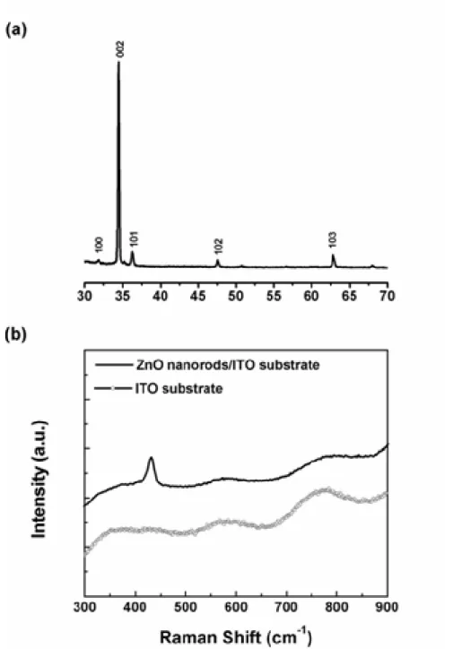
Figure 3-2. A schematic illustration for ZnO nanorod growth on nanostructured substrate by soft chemical method. (a)-(b) formation of ZnO nanoparticle colloids through sol-gel reaction and dispersion on ITO substrate; (c) the ZnO nanorods directly grow from the nanoparticles via hydrolysis-condensation process………...….43 Figure 3-3. (a) Absorption spectra, (b) TEM image and (c) XRD pattern of
CATOH-capped ZnO nanoparticles………..44 Figure 3-4. SEM images of ZnO nanorods grown inaqueous solution on the
nanostructured substrates. The corresponding concentration of Zn2+ aqueous solutions is (a) 10×10-3, (b) 8.4×10⁻³ and (c) 6.8×10⁻³ M. The inset in Fig. 3-4(a) exhibits hexagonal prismatic cross-section and a hemispherical end……….45 Figure 3-5. (a) XRD pattern and (b) Raman spectrum of the ZnO nanorods on ITO
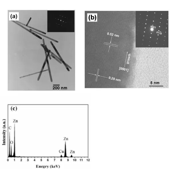
substrate……….46 Figure 3-6. (a) TEM and select area diffraction image of single crystal ZnO nanorods
grown in 10×10-3 M Zn2+ aqueous solution. The diffraction pattern shows that the nanorod grows along [0001] direction. (b) High resolution TEM image obtained from the edge of an individual nanorod and its corresponding SAED diffraction pattern (inset) (c) EDS analysis of ZnO nanorod………..47 Figure 3-7. PL spectra of (a) the as-grown ZnO nanorods and (b) heat treated at 350 oC for 12 h……….48 Figure 3-8. (a) SEM and (b) TEM images of the ZnO nanorods grown under same
condition but using precursor concentration of nanoparticles seeds about 0.05M………...………49 Figure 3-9. SEM image of the ZnO nanorods grown at the same condition but using the
nanostructured substrate with low heat treatment temperature of ~250
oC...49 Figure 3-10. SEM image of the ZnO nanostructure grown at the same condition but
using the nanostructured substrate with low heat treatment temperature of
~200 oC………..……..50
Figure 3-11. (a) A low magnification TEM image of as-synthesis ZnO nanotubes, (b,c) high magnification TEM images of a single nanotube, and (d) a HRTEM image of ZnO nanotube………...51
Arrays
Figure 4-1. SEM images show highly aligned ZnO nanotip arrays grown on the ZnO thin film at 95 oC aqueous solution for 6 hours. Low-magnification images from (a) top view and (b) tilt view reveal that high density of well-oriented ZnO
nanotips were dispersively distributed on the substrate. (c) Top and (d) side view of high-magnification SEM images. (e) TEM image of a typical ZnO nanotip. (f) High-resolution TEM image taken from the edge of ZnO nanotips and the corresponding fast Fourier-transform pattern (inset)………..62 Figure 4-2. Low density ZnO nanotip arrays grown on thin film with low concentration of 3×10 -4 M Zn2+aqueous solution………..63 Figure 4-3. SEM image showing the nanotips bundling together grown on the ZnO thin film at 95 oC aqueous solution for 24 hours………....63
Figure 4-4. X-ray diffraction pattern of ZnO nanotip arrays grown on the ZnO film..64 Figure 4-5. PL spectrum of ZnO nanotip arrays measured at room temperature…….65 Figure 4-6. High resolution TEM cross-section micrograph of the interface region...66 Figure 4-7. (a,b) SEM images show the as-grown ZnO nanotip arrays self-organized on
the ZnO microrod. (c) Bright-field and (d) dark-field TEM images from the nanotips-microrod junction region and (e) the corresponding diffraction pattern of microrod………..……..67 Figure 4-8. SEM images showing novel geometric structures of ZnO (a) nanopaintbrushs
and (b) nanopencils (c) nanorods/nanoplate………….………..68 Figure 4-9. Schematic diagram of experiment setup to study field-emission properties of
ZnO nanotips arrays………69 Figure 4-10. (a) Field emission current density vs electric field of ZnO nanotip arrays on Si
substrate and (b) the corresponding F-N plot……….…………..70
Chapter 5 Effect of Surface Stabilization of Nanoparticles on Luminescent
Characteristics in ZnO/Poly(hydroxyethyl methacrylate) Nanohybrid Film
Figure 5-1. TEM image and size distribution histogram of fresh unmodified ZnO particles………...…….89
Figure 5-2. Time dependence of UV/vis absorption spectra: (a) umodified ZnO
nanoparticles and (b) TPM-modified ZnO nanoparticles in ethanol. Inset are photographs of the ZnO nanoparticle colloids aging at room temperature for 2 months………..90 Figure 5-3. Particle diameters versus aging time of the ZnO particles in ethanol……..91 Figure 5-4. Powder x-ray diffraction spectra of (a) umodified ZnO nanoparticles, (b)
TPM-modified ZnO nanoparticles prepared with different aging time. The diffraction pattern of wurtzite ZnO crystal from JCPDS database is shown in bottom for comparison………92 Figure 5-5. FTIR spectra of the (a) unmodified ZnO nanoparticles and (b) TPM-modified
ZnO nanoparticles………..……….93 Figure 5-6. 1H NMR spectra of the (a) pure TPM stabilizer, (b) unmodified ZnO
nanoparticles and (c) TPM-modified ZnO nanoparticles dispersed in
DMSO-d6………95
Figure 5-7. Photoluminescence spectra of unmodified ZnO nanoparticles in ethanol solution., and modified and unmodified ZnO/PHEMA nanocomposites…96 Figure 5-8. Photographs of transparent ZnO/PHEMA nanocomposites with various
particles sizes (a) under daylight and (b)−(d) under an UV lamp. The luminescence images of nanocomposites fabricated by ZnO particles with an average diameter of (b) 3.2 nm; (c) 2.2 nm; and (d) 6.1 nm, respectively…97 Figure 5-9. Cross-section TEM images: (a) 6.1 nm unmodified ZnO particles in PHEMA matrix and (b) 3.2 nm TPM-modified ZnO particles in PHEMA matrix…..98 Figure 5-10. Photographs of ZnO/PMMA nanocomposites (a) under daylight and (b) under
an UV lamp with the samples of (I) 3.2 nm unmodified ZnO, (II) 3.2 nm TPM-modified ZnO and (III) 6.1 nm unmodified ZnO………..……..99
Chapter 1
Introduction
1.1 Background
“There’s plenty of room at the bottom, that...almost any chemically stable structure, that can be specified, can in fact be built….”
Richard P. Feynamn [1]
Since the famous statement by Richard P. Feynman in a talk to the American Physical Society nearly 50 years ago, there has been driving force toward the fabrication of materials using the synthesis routes that build molecules from the level of “bottom-up” synthesis. The “bottom-up” synthesis is considered to give more control over the structure and design of nanomaterials than the “top-down” synthesis, in that one starts with bulk materials and sculpts downward to get to the nanoscale.
Chapter 1 Introduction
“Top-down” Approach
“Top-down” approach has been enormously successful, as the evidence by the progress in the microelectronic industry [2]. The technology is partly dominated by the ever shrinking of devices in the semiconductor progress and supported by the availability of characterization. The trend of decrease device dimensions has followed the well-known Moore’s law [3] predicted in 1965 and illustrated in Figure 1-1. The figure shows that the dimension of a device halves approximately 18-24 months and today’s transistor were fallen in the nanometer range. The astonishing rate of progress will be difficult to continue much past 2010, however, due to a combination of technological and economic reasons. For instance, the widening of the band gap of semiconductors occurs when the size of materials reaches de Broglies’s wavelength.
Figure 1-1 “Moore’s Law” plot of transistor size versus year. [From ref. 4]
“Bottom-up” Approach
Another approach to nanofabrication is the so-called “bottom-up” approach. The approach refers to build-up materials from the bottom: atom-by-atom, molecular-by-molecules, or cluster-by-cluster. The approach has the potential to go far beyond of the limits of top-down technology by defining nanosystems through building structures molecules-by-molecules and even replication themselves.
Nanometer Scale Structures⎯Nanostructures
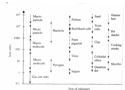
The development of structures with dimension in nanoscale range presents an exciting and rapidly expanding area of research in materials science. Figure 1-1 gives a partial list of zero-dimensional nanostructures, listing some of important objects from the microscopic to macroscopic world [4]. A “nano” represents one billionth, or 10-9. Generally, in a wider meaning of the nanostructures, any material that has at least one dimensions below 100 nm. Reducing 1, 2, 3, dimensions (D) of bulk materials to the nanometer scale produces nanometer thick 2D layer, 1D nanowires, 0 D nanoparticles, respectively.
Figure 1-2 Examples of zero-dimensional nanostructures with typical ranges of dimension. [From ref. 4]
Two-dimensional Nanostructures⎯Thin Film
Among nanostructures, thin film structures are the best developed, and many methods have been developed and improved. Different vapor-phase growth methods (such as evaporation , molecular beam, chemical vapor deposition, atomic layer deposition) and liquid-phase growth methods (such as electrochemical deposition , Langmuir-Boldgett, self-assembled monolayers, chemical solution deposition) have been developed to grow various thin films. These synthesis methods allow the intensive study of properties and application of many different materials.
Chapter 1 Introduction
One-dimensional Nanostructures⎯Nanowires, Nanorods
One-dimensional nanostructures, such as nanowires [5], nanorods … etc, have been the extensively studies due to their novel physical properties and potential to revolutionize broad area of nanotechnology. One-dimensional nanostructures are the smallest dimensional structures that can act both as interconnect for the transport of charge carrier, thus are ideally studied to the critical and ubiquitous task of moving charges in nanodevices [6,7]. As semiconductor nanowires, on the other hand, provide all the properties of traditional semiconductor, such as excellent optical and electric properties, as well as new benefits form the reduced dimensions of the materials, such as possible carrier mobility enhancement. However, compared with that in two-dimensional thin film systems and zero-dimensional nanoparticles, the research progress on nanowires has been rare, due to the difficulties associated with synthesizing nanowires with well-controlled composition. In general, the techniques employed to produce nanowires include thermal evaporation, chemical vapor deposition, anodic aluminum template, and hydrolysis reaction etc. The detailed description will be presented in Chapter 2.
Zero-dimensional Nanostructures⎯Nanoparticles (NPs)
Individual molecules, quantum dots, nanocrystals, and nanoparticles, which can be classified as zero-dimensional structures, are attractive building blocks for bottom-up approach of nanoscale devices. Although numerous techniques have been developed for synthesizing NPs, most practical application of nanomaterials will require high-quality suitable product (monodispersion, uniform shape, high stability of NPs).
Nanoparticles possess a large fraction of surface atoms per unit volume. Due to the vast surface area, all nanoparticle materials have a huge surface energy and, thus often form agglomeration as a result of attractive van der Waals force to minimize the total surface energy. In many applications and processing where well-dispersed particles or stabilized dispersion are required, and undesirable agglomeration and coagulation in the synthesis and processing steps must be prevented. Producing unagglomerated particles can be achieved by two conceptually different ways: electrostatic stabilization, and by steric stabilization [4].
Electrostatic Stabilization [8]
When the nanoparticles are ultra-small, and are dispersed in a polar solvent, van der Waals force and Brownian motion play important role, whereas the influence of gravity becomes negligible. The method is to disperse the particles by electrostatic repulsion resulting from the interaction between the electric double layers surrounding the particles. A typical example, the synergistic and concurrent particles preparation and electrostatic stabilization is illustrated by classical synthesis of 3 nm diameter ZnO particles [9]. This process involved the hydrolysis and condensation of ethanol zinc acetate dihydrate solution in lithium hydroxide monohydrate. The ZnO nanoparticles formed at coated by an electric double layer (composed of carboxylic acid ions and the cations of zinc) responsible for Coulombic responsible which decays exponential with increasing interparticles instance. There is a weak minimum repulsion in the van der Waals energy at an interparticle separation which approximately corresponds to the diameter of stabilized ZnO nanoparticles. The stable stable distance of particle separation depends not only on the charges of the particles, but also the concentration of ion in the diffuse region of the double layer. It also should be noted that electrostatic stabilization is limited by the following factors:
z It is only applicable to dilute systems.
z It is not applicable to electrolyte sensitive systems.
z It is almost not possible to redisperse the aggregated particles. z It is difficult to apply to multiple phase systems.
Steric Stabilization
One alternative way to produce unagglomerated particles is accomplished by absorbing polymer and/or surfactant onto the surface of nanoparticle colloids. This idea is borrowed from the physical basis of steric stabilization: a volume restriction effect arising from the decrease in possible configuration (entropy; ∆S) in the region between the two surface when the two particles contact one another and an osmotic effect due to the relatively high concentration of absorbed polymeric molecules in the region when the two particles.
Chapter 1 Introduction
Steric stabilization possesses several advantages over electrostatic stabilization [4]: z It is thermodynamic stabilization method, so that the particles are always redispersible. z A very high concentration can be accommodated, and the dispersion medium can be
completely depleted.
z It is not electrolyte sensitive.
z It is suitable to multiple phase systems
Size of Quantization Effects
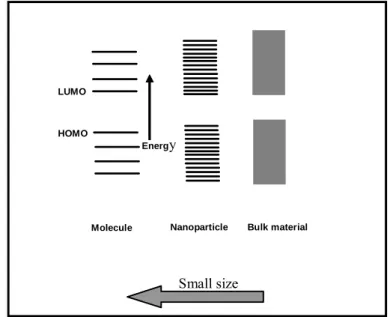
Dimensionality plays a critical role in determining the electronic and optical properties of materials. When the size of materials in a micrometer scale, the physical properties exhibit the same as that of bulk value; however, when the size of materials in a nanometer scale, the physical properties may exhibit a distinctively different from that of the bulk value. As a result, materials scientist interested in nanotechnology have mostly devote to the study of “the quantum-sized effects” owing to the spatial confinement of delocalized electrons in confined grain sizes. For example, bulk gold is chemically inert and thus considered to be not useful as a catalyst. However, nanostructured gold can have very excellent catalyst properties as first demonstrated by Haruta et al. [10]. Optical, mechanical, magnetic and thermal properties of nanostructured materials may also have similar shift. As an example is that the gold can appear blue, purple, red, or orange, as it size varies from 500 nm to 1 nm [11]. Similarly semiconductor (III-V) nanostructures exhibit a systematic blue-shift of photoluminescence emission when their size is smaller than 10−20 nm exciton diameter of corresponding bulk materials [12]. In the nano-size regime, these novel optical properties arise as a result of a change in the electric band structure. The energy states of a semiconductor material as it become in smaller size can be described initially as bulk material orbits which become discretely quantized band states in nanoparticles, and finally, quasi-uncontinuous energy bands in the molecule (Figure 1-3).
LUMO HOMO
Energy
Small size
Molecule Nanoparticle Bulk material
Figure 1-3 Energy level diagrams of three classes of materials showing discrete energies into molecules energy bands.
InorganicNanoparticles/Organic Polymer Nanohybrid
Recent extensive investigation into integration of organic and inorganic materials at nanoscale hybrid structures enables active devices that inherit the superior optoelectronic characteristic of nanoparticles (NPs) and possess advantages of polymers such as flexibility, film integrity, and conformity. The control of the particle size, size distribution and dispersion homogeneity over entire matrix is the critical prerequisite to assure the optical and electrical properties of the nanocomposites for nanodevice applications. Some of these applications for these nanohybrids materials are summarized in Table 1-1. It is apparent that the applications of nanohybrids range from electroluminescence to catalysis, solar cells, and storage.
Chapter 1 Introduction: Overview of the thesis
Table 1-1 Examples of some application of nanohybrids
Field Applications examples Reference
Device1: Ag/Mg:Ag/40 nmAlq3/CdSe (ZnS) NPs/TPD/ITO
EL: wavelength ~560 nm; external efficiency:~ 0.52 %
[13] Electroluminescence
Device 2:Ca:Al/MEH-PPV: doped InAs-ZnSe NPs/ITO EL: wavelength 1000 nm−1300 nm; external efficiency:~ 0.5 %
[14]
Catalysits Pt nanoparticles for hydrogenation of cyclohexane with 100 % conversion
[15]
Device 1:Al/PPV: doped ZnO NPs/ITO [16]
Solar cells
Devices2: Au/PA-PPV/TiO2 NPs/ITO [17]
Magnetic Storage Fe2O3 nanoparticles in magnetic media storage [18]
1.2 Overview of the Project
Thesis Outline
The dissertation is divided into three parts: first part (chapter 1 to chapter 2), comprise introduction and literature review. The second part (chapter 3 to chapter 5), describes the experiments, results, and discussions. The last part (chapter 6), presents a brief summary.
This thesis is organized in the following manner:
z In chapter 2, I describe a series of methodology used to produce one-dimensional ZnO nanostructures.
z In chapter 3, I present a soft chemical method for growth of single crystal ZnO nanords directly grown on ZnO nanostructured substrates. The structures, appearances and optical properties of ZnO nanorods also have been characterized in this chapter.
z In chapter 4, I further use the soft chemical approach to grow vertical and isolated single crystal ZnO nanotip arrays on different ZnO substrates. Results of optical and field emission measurement on ZnO nanotip arrays will also be presented.
z In chapter 5, I present the synthesis of high transparent and stable luminescent ZnO/PHEMA nanocomposites via a nanoparticle surface modified method. The characteristics of TPM-modified and unmodified ZnO nanoparticles have been characterized by UV-vis, XRD, TEM, FTIR and 1H NMR analysis.
1.3Reference
[1] R. Feynman. There’ plenty of room at the bottom: an invitation to center a new field of physics. Engineer & Science Magazine, California Institute of Technology, USA; 1960. [2] J. R. Health, P. J. Kuekes. G. S. Sinder, R. S. Williams, Science 280 (1998) 1716. [3] B. E. Deal, Interface 6 (1976) 18.
[4] G. Z. Gao, Nanostructures & Nanomaterials, Synthesis, Properties & Nanomaterials, Imperical College Press, 2004.
[5] M. H. Haung, Y. Wu, H. Feick, N. Tran, E. Webber, P. Yang, Adv. Mater. 13 (2001) 113. [6] Y. Wu, R. Fan, P. Yang, Int. J. Nano. 1 (2002) 1.
[7] Y. Wu, H. Yan, M. Huang, B. Messer, J. H. Song, P. Yang, Chem. Eur. J. 8 (2002) 1260. [8] P. C. Pierre, Introduction to Sol-Gel Processing, Kluwer, New Work, 1981.
[9] L. Spanhel and M. A. Anderson, J. Am. Chem. Soc., 113 (1991) 2826. [10] M. H. Hartua, Catal Today 36 (1997) 153.
[11] J. P. Wilcoxon, J. E. Martin, F. Parsapour, B. Wiedenman, D. F. Kelley, J. Chem. Phys. 108 (1998) 9137.
[12] C. B. Murry, D. J. Norris, M. G. Bawendi, J. Am. Chem. Soc. 115 (1993) 8706. [13] N. Tessler, V. Medvedev, M. Kazes, S. H. Kan, U. Banin, Science 295 (2002) 1506. [14] S. Coe, W. K. Woo, M. Bawendi, W. Bulovic, Nature 429 (2002) 800.
[15] A. B. R. Mayer, J. E. Mark, Colloid Poly. Si., 275 (1997) 333.
[16] W. J. E. Beek, M. M. Wienk, R. A. J. Janssen, Adv. Mater. 16 (2004) 1099. [17] A. C. Arango, L. R. Johnson, V. N. Bliznyuk, Z. Schlesinger, S. A. Carter, H. H.
Horhold, Adv. Mater. 12 (2000) 1689.
[18] D. Y. Godovsky, Biopolymers/PVA Hydrogels/Anionic Polymerization Nanocomposites, 153 (2000) 163
Chapter 2
Literature Review
This chapter first reviews the progress achievements in the synthesis of one-dimensional nanostructures materials. Based on the different media in the reaction system, the synthesis methods can be generally grouped into two major categories: vapor-based growth and liquid-based growth. Over the past two decades tremendous efforts have been carried out in the field of synthesis carbon nanotubes and 1D semiconductor materials, thus, our review in this chapter will be only focused on 1D ZnO nanostructures. Finally, a brief introduction of physical properties and potential application of 1D ZnO nanostructures are also described.
2.1 Strategies for Synthesis 1D ZnO Nanostructures
Since the successful synthesis of micron-size whiskers using chemical reaction under vacuum in the early 1960’s [1], the investigation and formation of one-dimensional nanostructures have attracted considerable attentions. Up to date, many techniques have
nanotechnology.
Table 2-1 summarizes the different processing techniques available for synthesis
Route Nanostructured Reference
one-dimensional ZnO nanostructures.
Methodology Processing Materials Wires -B Growth Template Growth Growth [2-10] Belts [11-13] Rods [14-17] Thermal Evaporation Tubes [17-20] Wires [21-24] Rods [25-29] Tubes [30-31] Belts [32] Vapor ased
Chemical Vapor Deposition
Needles [33-35]
Anodic Alumina Oxide Wires [36-37]
Dissolution-Condensation Rods [38] Wires [39] Rods [40-43] Liquid-Based Hydrolysis Reaction Tubes [44]
Vapor-based Growth
In this section, two vapor-based methods for preparing 1D ZnO nanostructures are introduced: the thermal evaporation, and chemical vapor deposition.
2.1.1 Thermal Evaporation
Since Sears was the first to explore the preparation of micro-size mercury whisker by axial screw dislocation in 1955, thermal evaporation has become one of the most commonly employed in the synthesis of 1D nanostructure materials. Nowadays, the thermal evaporation growth (vapor-solid process) has been widely used to synthesize a variety of ZnO nanostructures [2-10]. In principle, the thermal vaporization is a simple process in which the vapor is generated by vaporization; subsequently the resultant vapor transports and direct condenses the growth of species on the desirable substrate.
A typical example of 1D ZnO growth via the vapor-solid mechanism was reported by Wang and co-workers (see Figure 1a) [4]. A horizontal tube furnace of 50−100 cm length is used. Vaporization process is conducted in argon from several ten torr to ~600 torr. The powder sources are placed in an aluminum boat and holding at a high temperature of approximately 800−1400 oC to flow the source into the tube, some of which condense in the form of novel ZnO nanostructures (see Figure 2-1b) [4,45]. The morphology of products depends on the processing parameter, i.e, growth temperature, pressure, substrate, and atmosphere. The growth of 1D ZnO via thermal evaporation process may be involved with impurity metal.
Figure 2-1 (a) Schematic diagram of experimental apparatus for growth nanostructures by thermal evaporation growth. (b) SEM images of ZnO nanostructures. [From ref. 4, 45]
Chapter 2 Literature Review: Strategy for synthesis 1D ZnO nanostructures
2.1.2 Vapor-Liquid-Solid Growth Mechanism
-based methods, the vapor-liquid-solid (VLS) process seems to be the most
of micron-sized silicon whisker in 1960s. In the VLS mechanism, metal catalysts are used to form liquid alloys reactants. The anisotropic growth of nanowire is mainly indu
layer of metal catalyst (I); nucleation formation of the nano-sized liquid alloy droplet (Zn:Au) (II) a
Among the vapor
effective method for creating 1D nanowires with single crystalline structure. Wanger
et al. [46] first proposed the VLS mechanism to explain the growth
with dissolution of gaseous
ced and promoted by the solid-liquid interface energy of liquid droplets.
The impurity metal, such Au [2], Sn [47], Co, [48] and NiO [21] are known to be catalyst for guiding ZnO nanowires growth on to a specific substrate. The method of growing ZnO nanowires via VLS mechanism has been well adopted by Yang et al., [2] mainly relying on Au catalyst-induced anisotropic growth of nanowires. They explained the catalyst-induced growth process involving three stages (see Figure 2-2): deposition a
nd growth of ZnO nanowires from the supersaturation droplets of reactants by the VLS mechanism (III). The temperature of formation the liquid alloy droplets should be as high as 880−1000 oC when using Au as catalyst.
Au Alloy Zn vapor I II Substrate nanowir Zn vapor III IV
Figure 2-2 Scheme diagram of ZnO nanowires growth with Au particles as seeds for vapor-liquid-solid (VLS) mechanism. (I) Deposition of nano-sized Au particles on a Si substrate. (II) Formation a liquid alloy after heating to about 880 oC in a Zn and CO/CO2 vapor. (III) After the alloy reaching a supersaturated with vapor sources, the nuclei of
wires grown on Si (100). [From ref. 2]
ZnO crystals precipitate and further grow into the nanowires. (IV) SEM image of ZnO nano
The size of catalyst is recognized to be closely related the diameter of the nanowires, so that small size of metal cluster produces a small size nanowire [2]. By optimizing the growth condition and superior properties of metal catalysts, the possibility of thermal evaporation growth of quantum-sized ZnO nanostructures was suggested. For example, the extraordinarily small size of single crystalline ZnO nanobelts with an average width of 5.5 nm has recently been reported via a solid-vapor deposition process, in which nanobelts deposits on the silicon substrate coated with a thin layer of tin catalyst under a 250~300 oC and
nanowires on the substrate and allows for rmation patterns of ZnO nanowires [2,3]. By combining the selected area deposition of atalyst, ZnO nanowires have been grown as forests of vertically aligned ZnO nanowires ee Figure 2-3B). This process has two main disadvantages: the aligned nanowires are quired at relative high temperature (> 880 oC) growth and expensive sapphire substrates strict the large-scale production and wide applications of 1D ZnO arrays.
250~300 bar environment [49].
Sapphire is an ideal substrate to generate aligned ZnO nanorods on the substrate surface. The sapphire substrate has lattice constant a = 4.57 Å, c = 12.94 Å and small lattice mismatch (~0.1 % at room temperature) with ZnO. It has been proved that single crystalline nanorod can grow parallel to each other and perpendicular to the substrate surface (see Figure 2-3), owing to good epitaxial growth interface between the (0001) plane of ZnO crystal and the (110) plane of sapphire. Nowadays, the VLS mechanism is extensively applied to control the growth direction of
fo c (s re re
Chapter 2 Literature Review: Strategy for synthesis 1D ZnO nanostructures
2.1.1
approach, the active gaseous molecules are generated and transported into reaction chamber. The gaseous molecules will be either thermal disso
e vaporizing mperature of precursor can be maintained at temperature as low as 130−140 oC. Park et
l. [33] also employed this interesting method to form vertically well-aligned ZnO
anoneedles on (111) Si substrates, where the needles with sharp tips and uniform istribution in their diameter. Furthermore, a number of hosts have been extensively used
e MOCVD method to develop a controllable in suit doping of manganese in ZnO nanorods, hile it still maintaining wurtzite structure [35,50].
Similar to route of MOCVD, the preferentially aligned ZnO nanorod arrays can also be
chie s a
igher crystallography quality and a greater tendency to form regular arrays on the sapphire 001) substrate than those reported using other vapor-based method. Due to more
.3 Chemical Vapor Deposition (CVD)
The temperature for preparing aligned ZnO nanowire arrays via the VLS process is too high and not suitable for the fabrication of aluminum-based metallization of electronic devices (melting point of aluminum ~700 oC). As a result, it is desirable to grow aligned 1D ZnO arrays in a controlled low-temperature growth fashion.
CVD is of particular interest since it has a powerful approach for crystal film growth at a relative low temperature. In this
ciation or chemical reaction on a heat substrate surface to form stable solid film. Generally, CVD can be classified according to the type of heating method, such as thermally activated CVD, photo-assisted CVD, plasma-enhanced CVD (PECVD), metal-organic chemical vapor deposition (MOCVD) and mtalorganic vapor-phase epitaxial growth (MOVPE). Wangrt and Eillis was the first used the CVD method to grow whisker in 1964 and then Givargizov extended this method to synthesize a variety of whiskers (such as Ge, GaAs, InP and Si).
Recently, Wu’s group [25] was among the first of several groups that developed and optimized a related metal-organic chemical vapor deposition (MOCVD) method to obtain aligned ZnO nanorods on silicon and sapphire substrate at ~500 oC. By employing zinc acetylacetonate hydrate compound as the metal-organic precursor, th
te a n d th w
a ved by MOVPE, according to Park et al. [51]. In this method, the nanorods posses h
f growth conditions obtained in the reaction cham
ecently, this method has been used to fabricate nanocsale multiple-quantum-well heter
uniform vaporized gas and better control o
ber, the diameter of nanorods can be effectively controlled by varying the reaction time. A drawback of this method is that it needs to operate in the low-vapor-pressure. Therefore, expensive vacuum equipment is required.
R
ostructures of ZnO/ZnOMgO nanords arrays (see Figure 2-4) [52]. These quantum structures in a single nanorod would enable novel physical properties from quantum confinement effect.
(a) (b)
Liquid-based Growth
In this section, three liquid-based growth methods have been used to prepare a number of 1D ZnO nanostructure materials: including anodic alumina oxide template, orient-attachment growth, and hydrolysis reaction. In contrast to the techniques discussed above, the liquid-based method has several advanta
Figure 2-4 (a) Schematic of 10 periods of MQWs ZnO nanorods grown on the sapphire substrate. (b) SEM image of the MQWs ZnO nanorods. [From ref. 52]
ges, such as environment friendliness, easily large scaling, low producing cost, and low-temperature growth condition.
Chapter 2 Literature Review: Strategy for synthesis 1D ZnO nanostructures
uniform, cylindrical pores with diameter ranging from 0 nm to 200 nm (I). The pores are arranged in regular hexagonal arrays and the pore dens
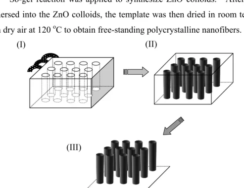
mbrane (II). If the template of membrane is dissolved in a chemical olution, the free-standing nanowire arrays are obtained (III). Although the AAO
mplate-assisted method has been demonstrated to be efficient approach of large-area (up to everal cm2) nanowire arrays, it still has a dr ack. Most of the AAO-template synthesis f nanowires is polycrystal or amorphous structures. The polycrystalline/amorphous anowires could be severely limited their application in optoelectronic nanodevices.
Martin and co-workers [37] recently reported that high density of ZnO nanofibrils with n average diameter of 200 nm were fabricated by filling ZnO colloidal solutions into AAO mplate. So-gel reaction was applied to synthesize ZnO colloids. After the membrane as immersed into the ZnO colloids, the template was then dried in room temperature, and red
2.1.4 Anodic Alumina Oxide (AAO) Template
Among the numerous liquid-based methods, anodic alumina oxide (AAO) template has attracted interesting due to its versatility and facility. Anodic alumina oxide is a thermally and chemically stable template; that has
1
ity can be as high as 1011 pores per square centimeter. In this technique, the high density nanochannels can be filled with metals or semiconductor materials by pressurized liquid injection, polymerization, sol-gel colloids and electrochemical deposition to form 1D nanowires in the me s te awb s o n a te w
it in dry air at 120 oC to obtain free-standing polycrystalline nanofibers.
(I) (II)
fi
(III)
Figure 2-5 Schematic outlines of fabrication free-standing nanowire arrays by AAO template method.
2.1.5 Orient-attachment Growth
Nanocrystals growth in solution generally comprises the fast nucleation of primary particles and the subsequently crystal growth via two primary mechanism of coarsening and aggregation processes. Penn and Banfield [53] proposed a new crystal growth mechanism called “orient-attachment” growth in which the anatase and iron oxide can coalesce together under hydrothermal condition. In the nanocrystals aggregates process, the lattice plane at the interface of adjacent oriented particles may not perfectly align and result in a dislocation at the contact particles. These defects would influence subsequent ocarsening and final structures of crystal.
Single crystal ZnO nanorods can also be formed via a self-assembly mechanism of aggregated nanoparticles in methanol, as Weller et al [38] has demonstrated in recent year. This approach uses an extremely simple, low-temperature (60
s with ize of ~3 nm through a sol-gel reaction (Figure 2-6a). The concentration of colloids was then
h aggregated anoparticles e as seeds for further crystal growth. The “orient-attachment” growth has
e advantages of producing nanorods very quickly and massively. However, the control of ucleation site and orientation of the nanorods on the substrate would be very difficult.
Hydrothermal synthetic route is similar to orient-attachment method. It also has been explored as another possible way to produce single crystal ZnO nanorods by liquid-based reaction. In this process, a mixture of alkali aqueous solution and complex agent such as ethylenediamine is put into the Telfon-lined autoclave, where the complex agent are usually used to control the growth rate of different faces. The whole reaction are kept at evaluated temperature (180−230 oC) and pressure (0.1−15 MPa) environment to lead ZnO crystal
gr ZnO
nanorods with high crystalline in the diameter regime of 50 nm under a high-pressure and oC), liquid-based growth. The first step of this approach involved the formation of the quasi-spherical particle
s
increased by evaporation of the solvent and aged at 60 oC in different length of time. Specifically, the length of rod-like nanoparticles increased with reaction time, but the width of nanorods grew only slightly (see Figure 2-6b). This process thus enables the single crystalline ZnO nanorods to grow in the absence of a template. Weller used an “oriented attachment” mechanism to explain anisotropic growth of nanorod, in whic
n serv
th n
Chapter 2 Literature Review: Strategy for synthesis 1D ZnO nanostructures
of Zn alkali.
up 5] proposed a metal-oxide crystals growth method called “purposed-built materials” or we calle m l p t a n q d
very well, which will be the focus in our research. high-temperature (180 oC) solutions
(a) (b)
2.1.6 Hydrolysis Reaction
Despite the described progress of the liquid-based methodology for synthesis single crystal 1D ZnO, there is still remained some problems in their synthesis, such as mass production and well aligned growth of ZnO on the substrates. But, the Vayssieres’s gro
Figure 2-6 Schematic illustrating the formation of ZnO nanorods by “oriented attachment” growth: (a) fresh nanoparticles and (b) after one day aging at 60 oC of the concentrated colloids.
[5
d “soft chemical route”, as a new candidate for growing single crystals ZnO. This ethod is capable of controlling growth directly on the substrate and acquiring a arge-scaled production of 1D ZnO arrays. In additional, these ordered ZnO arrays can
repare by hydrolysis reaction of zinc salt precursor in an aqueous at attractive low emperature of 95 oC. Since the electrical and optical properties of 1D ZnO nanostructures
re size-dependent, the growth of high crystal quality ZnO with well-defined and anometer-sized diameter is highly desirable. The soft chemical route can obtain large uantities of ZnO submicrods, however, the product size and morphology can not controlle
ucleation and Growth Model N
The easiest method to prepare uniformly sized colloids metal oxide is based on (forced) ydrolysis of metal salt solution. The monodispersive particles can be obtained by arefully controlling the kinetics of the precipitation in ionic solution. It is well known that
ost polyvalent cations readily hydrolyze, and that deprotonation of coordinated water olecules is greatly accelerated with increasing temperature. Therefore, increasing mperature will result in an increasing amount of deprotonated molecules because ydrolysis products are intermediates to the precipitation of metal oxides.
In the formation of new crystal from solution, the nucleation plays an important role in ontrolling the final particles size and distribution. Essentially, there are three kind of ucleation process: homogenous nucleation, heterogeneous nucleation and secondary u
u f
u
In the classical theory of homogenous nucleation, the overall free energy change (∆G) r spherical particles, is the sum of the free energy of formation of a new volume and free
on. h c m m te h c n
n cleation. Homogenous nucleation occurs in the absence of any solid interface, as cleating acid. On the other hand, heterogeneous nucleation allows the formation o
lei on the foreign solid interface. c
n n
fo
energy of new surface creati
∆G = −4/ν ⋅π⋅r3⋅k
B⋅T⋅ln (S) + 4 π⋅r2γ
Where ν is the molecular volume of the precipitated particle, r is the radius of the embryo, kB is the Boltzmann’s constant, S is the saturation ratio and γ is the surface free energy per unit surface area.
Once the solution reaches a saturation ratio (S > 1), ∆G has a positive maximum at a critical size. This maximum free energy is the activation energy for nucleation. In the most case of metal oxide, however, homogenous nucleation in the absence of a solid interface solution needs a higher activation energy barrier. Therefore, the heterogeneous
Chapter 2 Literature Review: Properties and Potential Applications
ucleation mechanism will be more favorable to crystal growth in the solution. Based on , the crystal nucleation and growth in the solutions are cont
ynthesis 1D ZnO nanostructures as mentioned above. One signification for literature review in this chapter is the
uides, varistors, gas senosor, surface acoustic wave devices, transparent conducting glass and field emission devices.
tzite (hexagonal; space group C6mc) structures with lattice onstant a = b= 3.25 Å and c = 5.12 Å, where layers occupied by zinc atoms alternate with
layers occup oms are tetrahedrally coordinate to four
xygen atoms, and the d-electrons of zinc hybridize with the p-electron of oxygen (see Fig
n
the model of hetero-nucleation
rolled by interface free energy. Generally, the interfacial energy between the crystal and the substrate is smaller than the interfacial energy between the crystal and the solution. When the reactant species is a supersaturated, thereby a new crystal only forms on the substrate.
2.2 Properties and Potential Applications of 1D ZnO Nanostructures
In this chapter, we have been focused on studying the issue of s
physical properties and potential applications for 1D ZnO nanostructures.
Zinc oxide has been know and extensively studied over the past two decades. ZnO is a very promising material for optical, electrical, catalytic and piezoelectric applications. Therefore, it has emerged as one of most used semiconductor oxides employed in catalysts, solar cell, UV LEDs, optical waveg
2.2.1 The Structures and General Properties of ZnO
Zinc Oxide (ZnO) has a wur c
ied by oxygen atoms. The zinc at o
ure 2-7).
nts. Cd substitution (doping) can lead to a reduction in the energy gap to ~ .0 eV, whereas Mg substitution can increase the energy gap to as high as ~4.0 eV [58].
nd the hole
ately, both ZnO film and 1D ZnO single crystalline nanostructures show excellent optic
perature (26 meV). As such, it offers a candidate host for developing a room temperature UV laser [3].
-1) than GaN (100 cm-1) at room temp
d possible quantum confinement effect that may exhibit new distinct electrical, chem thermal properties. At present, many researches have been extensively devoted to explore these novel physical properties and take advantage of these
roperties in advanced nanodevice applications.
Recent progress in processing and novel applications for related 1D ZnO nanomaterials re listed below:
To realize any type of devices technology, it is difficult to understand their character without a basic knowledge of basic material parameters. Table 2-2 summarizes the material parameters of wurtzite ZnO [57]. ZnO is an II−VI compound semiconductor with direct band gap of 3.4 eV at room temperature, and shows optical properties similar to observed in GaN. The optical band gap of ZnO can be tuned via divalent substitution on the cation site, as called dopa
3
The electron Hall mobility in single crystal ZnO is between 100 and 200 cm2/V s a
Hall mobility is on the order of 5 cm2/V s at room temperature. The carrier effective mass in ZnO is basically equal to 0.24 m0 and 0.59 m0 for electrons and holes, respectively.
L
al characteristics. In some respects, the physical properties of ZnO compare favorably to those of the GaN. The high exciton binding energy (60 meV) in ZnO wurtzite crystals, significantly larger than that of GaN (25 meV), that ensures an efficient exciton relate photon emission process under low threshold excitation energy at room temperature. The binding energy of ZnO has greater than thermal energy at room tem
Furthermore, ZnO has higher optical gain (300 cm erature.
2.2.2 Application of 1D ZnO Nanowires
In contrast to bulk materials, the low-dimensional nanoscale materials comprise large surface area an
ical, optical, and
p
Chapter 2 Literature Review: Properties and Potential Applications
Fabrication of p-GaN/n-ZnO nanorods heterojunction EL devices [60] z Synthesis single-crystal ZnO nanowires via a VLS growth mechanism [2,3] z Room temperature ultraviolet lasing in ZnO nanowire arrays [3]
z Growth aligned submicron ZnO rods in low-temperature aqueous solution [55] z Field electron emission from vertically aligned ZnO nanowire arrays [59]
z Synthesis of single-crystal complete nanorings of ZnO via a spontaneous self-coiling process [56]
z Quantum confinement observed in ZnO/ZnMgO nanorods heterostructures [52] z
Hydrogen Storage
Hydrogen storage in 1D nanostructure, such CNTs, has attracted a great deal attention. Hydrogen storage capacity would be potentially useful for fuel cell in electric vehicles or laptop computer application. Recently, Wan et al. [61] have reported that the hydrogen storage capacity of about 0.83 % is achieved in ZnO nanowires under the pressure of 3.03 Mpa at room temperature and about 71 % of the storage hydrogen is released under ambient
ressure.
Gas Sensors
p
Among major application of 1D ZnO nanostructures is likely related the sensing of gas molecules. Because of the high surface-to-volume ratio of 1D ZnO nanostructures, their electronic properties are extremely sensitive to species absorbed on the surface. For example, Wang and co-workers [62,63] have demonstrated the perspective of gas sensor using the microelectromechanical system based on ZnO nanowires. They reported that ZnO nanowires have a high sensitivity and fast
oC. In another demonstration, the same group also observed that the response to ethanol gas molecules at a work temperature of 300
positive temperature coefficient resistance of Cd-doped ZnO nanowires strongly depends on doped ZnO porous surface states produced by water molecules absorption. Hence, the
Cd-nanowires might show a promising application for humidity sensors.
Field-emission Devices
Because of the unique geometries of 1D nanowires and nanotubes, combined with their
active as cold
high flexibility and hardness resulting from defect-free lattices, these materials are attr cathode for device that use field emission electron sources and flat panel
ission anowire arrays exhibited a turn-on electric field of about 6.0 V/µm and the emission current density reached about 1 mA/cm2 at an applied field of 11.0 V/µm.
field in the tetrapod-like ZnO nanostructures
carbon nanotubes emitters. The field emission properties in various ZnO anostructure emitters are summarized in Table 2-3.
Elec
display. Le and co-workers [59] were first group to explore the field em characteristics of well-aligned ZnO nanowires. The single crystalline n
Wan et al. [64] have reported the turn-on
almost as low as 1.6 V/µm at the current density of 1 µA/ cm2. Ren et al. [65] subsequently developed an extremely low operating electric field of ZnO nanowires grown on carbon cloth. In particular, a turn-on electric field of as low as 0.7 V/µm is needed to obtain an emission current density of 1 mA/cm2, which is comparable with those for other field emitters as
n
troluminescence Devices
One of the more exciting applications for 1D ZnO nanowires is the light-emitting diodes (LEDs). Because of the superior characteristic of direct and wide band gap with a large exciton binding energy (60 meV), the ZnO materials are attractive much attentions especially for short-wavelength emitting devices application. Like ordinary electroluminescence devices, the ZnO-based EL device typically comprises ZnO p-n homojunction structure and n-ZnO/p-GaN heterojunction structure. The latter generates luminescence; however, has lower luminescence efficiency due to the large lattice mismatch at junction interface. This problem may be resolved by employing the growth 1D
Chapter 2 Literature Review: Properties and Potential Applications
nanorods, as nanosize junctions, since the growth mechanism of nanorods is completely different. Yi et al. [60] have demonstrated the electroluminescence from the p-GaN/n-ZnO nanorod arrays heterostructure EL devices (see Figure 2-8). The p-n heterojunctions
anorod arrays device shows a high current density and strong luminescence at a reverse- ias of 3V.
n b
igure 2-8 (a) Schematic illustration of p-GaN/n-ZnO nanorods heterostructures devices. (b) SEM image of as-synthesis ZnO nanorods on GaN substrate. [From ref. 60].
Table 2-2 Properties of wurtzite ZnO. [57] Property Value Lattice parameter at 300 K a0 0.32495 nm c0 0.52069 nm a0/c0 1.602 u 0.345 Density 5.606 g/cm3
Stable phase at 300 K Wurtzite
Melting point 1975 oC
Thermal conductivity 0.6, 1−1.2
Linear expansion coefficient (/C) a0: 6.5×10⁻⁶
c0: 3.0×10⁻⁶ Static dielectric constant 8.656
Refractive index 2.008, 2.029
Energy gap 3.4 eV , direct
Intrinsic carrier concentration < 106 meV
Exciton binding energy 60 meV
Electron effective mass 0.24m0
Electron Hall mobility at 300K for low n-type conductivity
100−200 cm2/V s
Hole effective mass 0.59 m0
Hole Hall mobility at 300 K for low
p-type conductivity
Chapter 2 Literature Review: Properties and Potential Applications
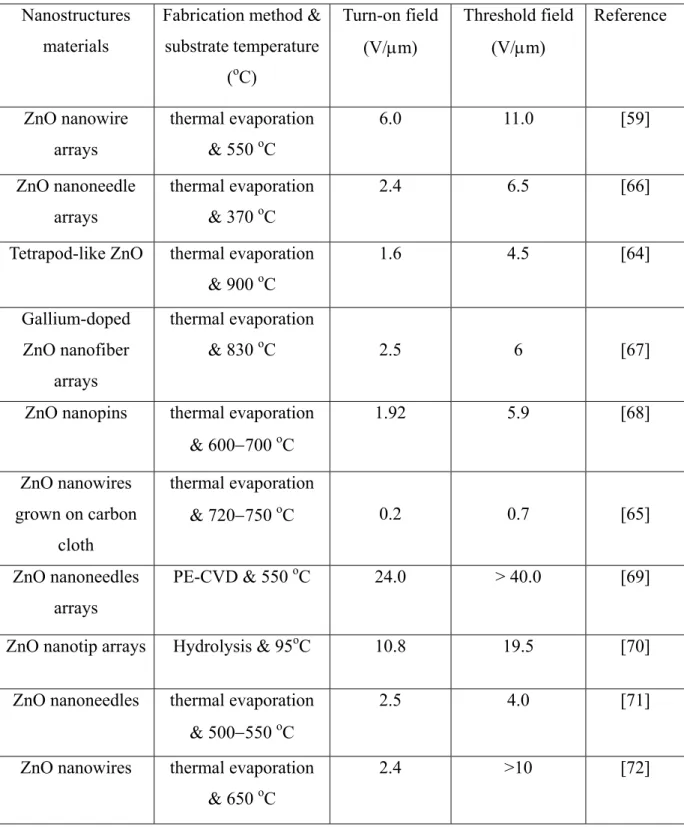
Table 2-3 Summary on turn-on fields and threshold fields (field required to generate a current mA/cm2, respectively) for various ZnO nanostructures emitters.
Nanostructures materials
Fabrication method & trate temperature (oC) Turn-on f (V/µm) old field (V/µm) Reference of emissi
density of 10 µA/cm2 and 1
subs ield Thresh & 550 therm o e thermal e & 370 o od-like ZnO thermal evaporatio
doped thermal evapor er & 83
anopins thermal evaporat & 600−700 cloth & 720−750 C thermal evaporation arrays Hydrolysis o ZnO nanowire arrays al evaporation C 6.0 11.0 [59] ZnO nanoneedl arrays vaporation C 2.4 6.5 [66] Tetrap n & 900 oC 1.6 4.5 [64] Gallium-ZnO nanofib arrays ation 0 oC 2.5 6 [67] ZnO n ion oC 1.92 5.9 [68] ZnO nanowires grown on carbon o 0.2 0.7 [65] ZnO nanoneedles arrays PE-CVD & 550 oC 24.0 > 40.0 [69]
ZnO nanotip & 95 C 10.8 19.5 [70]
ZnO nanoneedles thermal evaporation & 500−550 oC
2.5 4.0 [71]
ZnO nanowires thermal evaporation & 650 oC
2.3 Motivation
methods have rarely been achieved.
os he ro
diam O nan ctur nanopar
controlling the nuclei of them e nanometer scale at which they grow. In this way, the
Zn reate d “bott p” approach is characte of
nanotechnology. In the second purpose, we devote to grow highly aligned and free-standing ZnO nanotip arrays grown on the ZnO films. The soft growing method also
has been extended to synthe etric structures, including
nanotips/rod arrays, nanopaintbrushs and nanopencils. In the third objective, highly transparent and stable lum ly(hydroxyethyl methacrylate) nanocomposites have been synthesized via a nanoparticle surface modified method. The resulting
Z com odified nanoparticles have a better dispersibility
and controllable luminescent properties.
Even though several groups have been extensively working to develop 1D ZnO on the substrate by using vapor-based growth, to date successful preparing ZnO nanorods via the liquid-based
The first purp eter of Zn
e of this research is to orods on the nanostru
on th
use the soft c mical route to p duce small ed (ZnO ticles/ITO) substrates, by
O nanorod is c d using the recognize om u that ristic
size a series of novel geom
inescent ZnO/Po
2.4 Reference
[1]
[3]
[9] Y. W. Wang, L. D. Zhang, G. Z. Wang, X. S. Peng, Z. Q. Chu, C. H. Liang, J. Cryst. Growth 234 (2002) 171.
[10] S. C. Lyu, Y. Zhang, C. J. Lee, Chem. Mater. 15 (2003) 3294. [11] X. Y. Kong, Y. Ding, Z. L. Wang, J. Phys. Chem. B 108 (2004) 570. [12] X. Y. Kong, Z. L. Wang, Nano Lett. 12 (2003) 1625.
[13] R. S. Yang, Y. Ding, Z. L. Wang, Nano Lett. 4 (2004) 1309.
[14] Y. Dai, Y. Zhang, Q. K. Li, C. W. Nan, Chem. Phys. Lett. 358 (2002) 83. [15] J. Y. Lao, J. Y. Huang, D. Z. Wang, Z. F. Ren, Nano Lett. 3 (2003) 235.
[16] V. A. L. Roy, A. B. Djursic, W. K. Chan, Gao, H. F. Lui, C. Surya, Appl. Phys. Lett. 83 (2003) 141.
[17] H. Chik, J. Liang, S. G. Cloutier, N. Kouklin, J. M. Xu, Appl. Phys. Lett. 84 (2004) 3376.
[18] J. Q. Hu, Q. Li, X. M. Meng, C. S. Lee, S. T. Lee, Chem. Mater. 15 (2003) 305. G. W. Sear, Acta Metal, 3 (1955) 361.
[2] M. H. Haung, Y. Wu, H. Feick, N. Tran, E. Webber, P. Yang, Adv. Mater. 13 (2001) 113. M. H. Huang, S. Mao, H. Feick, H. Yan, Y. Wu, H. Kind, E. Weber, R. Russo, P. Yang, Science 292 (2001) 1897.
[4] Z. R. Dai, Z. W. Pan, Z. L. Wang, Adv. Funct. Mater. 13 (2003) 9. [5] B. D. Yao, Y. F. Chen, N. Wang, Appl. Phys. Lett. 81 (2002) 757.
[6] D. Banerjee, J. Y. Lao, D. Z. Wang, J. Y. Huang, Z. F. Ren, D. Steeves, B. Kimball, M. Sennett, Appl. Phys. Lett. 83 (2003) 2061.
[7] H. J. Yuan, S. S. Xie, D. F. Liu, X. Q. Yan, Z. P. Zhou, L. J. Ci, J. X. Wang, Y. Gao, L. Song, L. F. Liu, W. Y. Zhou, G. Wang, Chem. Phys. Lett. 371 (2003) 337.
[8] Y. C. Kong, D. P. Yu, B. Zhang, W. Fang, S. Q. Feng, Appl. Phys. Lett. 78 (2001) 407.
L. Zhang, D. P. Yu, Appl. Phys. Lett. 83 (2003) 1689.
[20] B. P. Zhang, N. T. Binh, K. Wakatsuki, Y. Segawa, Y. Yamada, N. Usami, M. Kawasaki,
[21] S. C. Lyu, Y. Zhang, H. Ruh, H. J. Lee, H. W. Shim, E. K. Suh, C. J. Lee, Chem. Phys.
[22] C. Y. Geng, Y. Jiang, Y. Yao, X. M. Meng, J. A. Zapien, C. S. Lee, Y. Lifshitz, and S. T. Lee, Adv. Funct. Mater. 14 (2004) 589.
[24] M.C. Jeong, B. Y. Oh, W. Lee, J. M. Myoung, J. Cryst. Growth 268 (2004) 149. J. J.
[26] B. P. Zhang, N. T. Binh, Y. Segawa, K. Wakatsuki, N. Usami, Appl. Phys. Lett. 83 (2003) 1365.
[28] S X. Liu, X. H. Wu, H. Cao, R. P. H. Chang, J. Appl. Phys. 95 (2004) 3141.
Aravind, D. H. L. Ng, Mater. Lett. 58 (2004) 2195.
Yamada, N. Usami, M. Kawasaki,
[31] J. J. Wu, S. C. Liu, C. T. Wu, K. H. Chen, L. C. Chen, Appl. Phys. Lett. 81 (2002) 1312.
[33] W. I. Park, G. C. Yi, M. Y. Kim, S. J. Pennycook, Adv. Mater. 14 (2002) 1841.
[34] , H. Sheng, J. Zhong, Z. Zhang, N. W. Emanaetoglu, Y. Lu, IEEE Trans.
[35] J. Zhang, S. Muthkumar, Y. Chen, Y. Lu, H. M. Ng, W. Jiang, E. L. Garfunkel, Appl. H. Koinuma, Appl. Phys. Lett. 84 (2004) 4098.
Lett. 363 (2002) 134.
[23] S. Y. Bae, H. W. Seo, J. H. Park, J. Phys. Chem. B 108 (2004) 5206.
[25] Wu, S. C. Liu, Adv. Mater. 14(2002) 215
[27] H. T. Yuan, Y. Zhang, J. Cryst. Growth 263 (2004) 119.
[29] G. Z. Wang, N. G. Ma, C. J. Deng, P. Yu, C. Y. To, N. C. Hung,M.
[30] B. P. Zhang, N. T. Binh, K. Wakatsuki, Y. Segawa, Y. H. Koinuma, Appl. Phys. Lett. 84 (2004) 4098.
[32] J. Zhang. W. Y. Yu, L. D. Zhang, Phys. Lett. A 229 (2002) 276.
S. Muthukumar
Phys. Lett. 83 (2003) 3401.
Y. Li, G. W. Meng, L. D. Zhang, F. Phillipp, Appl. Phy
[36] s. Lett. 76 (2000) 2011.
[38] hem. Int. Ed. 7 (2002) 41.
[40] angmuir 20 (2004) 4196. ong, Chem. 004) 986. [45] aterials Today 7 (2004) 26. [50] t. 85 (2004) 1027. 5 (2003) 526 0) 751.
[55] . Lindquist, A. Hagfeldt, J. Phys. Chem. B 105 (2001) [37] B. B. Lakshmi, P.K. Dorhout, C. R. Martin, Chem. Mater. 9 (1997) 857
C. Pacholski, A. Kornowski, H. Weller, Angew. C [39] L. Vayssieres, Adv. Mater. 15 (2003) 464.
B. Liu, H. C. Zheng, L
[41] J. Zhang, L. –D. Sun, X. –C. Jiang, C. –S. Liao, C. –H. Yan, Crystal. Growth & Design 4 (2004) 309.
[42] X. P. Gao, Z. F. Zheng, H. Y. Zhu, G. L. Pan, J. L Bao, F. Wu, D. Y. S Commun. (2004) 1428.
[43] B. Cheng, E. T. Samulski, Chem. Commun. (2
[44] L. Vayssieres, K. Keis, A. Hagfeldt, S. E. Lindquist, Chem. Mater. 13 (2001) 4395. Z. L. Wang, M
[46] R. S. Wanger, W. C. Ellis, Appl. Phys. Lett. 4 (1964) 89. [47] P. X. Gao, Y. Ding, Z. L. Wang, Nano. Lett. 3 (2003) 1315.
[48] C. J. Lee, T. J. Lee, S. C. Lyu, Y. Zhang, H. Ruh, H. J. Lee, Appl. Phys. Lett. 19 (2002) 3648.
[49] X. Wang, Y. Ding, C. J. Summers, Z. L. Wang, J. Phys. Chem. B 103 (2004) 9701. J. J. Wu, S. C. Liu, M. H. Wang, Appl. Phys. Let
[51] W. I. Park, D. H. Kim, S. –W. Jung, G. –C. Yi, Appl. Phys. Lett. 80 (2002) 4232. [52] W. I. Park, G. –C. Yi, M. Y. Kim, S. J. Pennycook, Adv. Mater. 1
[53] J. F. Banfield, S. A. Welch, H. Zhang, T. T. Ebert, R. L. Penn, Science 289 (200 [54] B. Liu, H. C. Zhang, J. Am. Chem. Soc. 125 (2003) 4430.
L. Vayssieres, K. Kesis, S. E 3350.
22 (2003)
ppl. Phys. Lett. 81 (2002) 3648.
[62] Li, Y. J. Chen, T. H. Wang, X. L. He, J. P. Li, C. L. Lin, Appl. Phys. Lett.
[63] en, T. H. Wang, X. L. He, X. G. Gao, J. P. Li, Appl. Phys. Lett.
Lett. 85 (2004) 1407.
Zhao, B. Xiang, R. M. Wang,
[68] u, X. W. Sun, Appl. Phys. Lett. 83 (2003) 3806.
[57] S. J. Pearton, D. P. Norton, K. Ip, Y. W. Heo, T. Steiner, J. Vac. Sci. Technol. B 932.
[58] L. K. Singh, H. Mohan, Indian, J. Pure Appl. Phys. 13 (1975) 222. [59] C. J. Lee, T. J. Lee, S. C. Lyu, Y. Zhang, A
[60] W. I. Park, G. –C. Yi, Adv. Mater. 16 (2004) 87.
[61] Q. Wan, C. L. Lin, X. B. Yu, T. H. Wang, Appl. Phys. Lett. 84 (2004) 124. Q. Wan, Q. H.
84 (2004) 3654.
Q. Wan, Q. H. Li, Y. J. Ch 84 (2004) 3085.
[64] Q. Wan, K. Yu, T. H. Wang, C. L. Lin, Appl. Phys. Lett. 83 (2003) 2253. [65] S. H. Jo, D. Banerjee, Z. F. Ren, Appl. Phys.
[66] Y. W. Zhu, H. Z. Zhang, X. C. Sun, S. Q. Feng, J. Xu, Q. D. P. Yu, ppl. Pys. Lett. 83 (2003) 144.
[67] C. X. Xu, X. W. Sun, B. J. Chen, Appl. Phys. Lett. 84 (2004) 1540. C. X. X
[69] Y. K. Tseng, C. –J. Huang, H. –M. Cheng, I. –N. Lin, K. –S. Liu, I. –C. Chen, Adv. Funct. Mater 13 (2003) 811.
[70] C. H. Hung, W. T. Wang, J. Cryst. Growth 268 (2004) 242. [71] Y. B. Li, Y. Bando, D. Golberg, Appl. Phys. Lett. 84 (2004) 3603 [72] S. Y. Li, P. Lin, C. Y. Lee, T. Y. Tseng, J. Appl. Phys. 95 (2004) 3711
![Figure 1-1 “Moore’s Law” plot of transistor size versus year. [From ref. 4]](https://thumb-ap.123doks.com/thumbv2/9libinfo/8760727.208117/14.892.220.732.525.797/figure-moore-law-plot-transistor-size-versus-year.webp)

![Figure 2-3 ZnO nanowires arrays grown on sapphire (0001) substrate. [From ref. 3]](https://thumb-ap.123doks.com/thumbv2/9libinfo/8760727.208117/27.892.245.683.814.1039/figure-zno-nanowires-arrays-grown-sapphire-substrate-ref.webp)
![Table 2-2 Properties of wurtzite ZnO. [57] Property Value Lattice parameter at 300 K a 0 0.32495 nm c 0 0.52069 nm a 0 /c 0 1.602 u 0.345 Density 5.606 g/cm3](https://thumb-ap.123doks.com/thumbv2/9libinfo/8760727.208117/39.892.162.721.145.938/table-properties-wurtzite-property-value-lattice-parameter-density.webp)