THz radiation emission properties of multienergy arsenic-ion-implanted GaAs and
semi-insulating GaAs based photoconductive antennas
Tze-An Liu, Masahiko Tani, and Ci-Ling Pan
Citation: Journal of Applied Physics 93, 2996 (2003); doi: 10.1063/1.1541105
View online: http://dx.doi.org/10.1063/1.1541105
View Table of Contents: http://scitation.aip.org/content/aip/journal/jap/93/5?ver=pdfcov
Published by the AIP Publishing
Articles you may be interested in
Analysis of terahertz pulses from large-aperture biased semi-insulating and arsenic-ion-implanted GaAs antennas
J. Appl. Phys. 104, 053121 (2008); 10.1063/1.2967716
Terahertz emission properties of arsenic and oxygen ion-implanted GaAs based photoconductive pulsed sources
J. Vac. Sci. Technol. A 24, 774 (2006); 10.1116/1.2183284
Dark current and trailing-edge suppression in ultrafast photoconductive switches and terahertz spiral antennas fabricated on multienergy arsenic-ion-implanted GaAs
J. Appl. Phys. 98, 013711 (2005); 10.1063/1.1953867
Ultrabroadband terahertz field detection by photoconductive antennas based on multi-energy arsenic-ion-implanted GaAs and semi-insulating GaAs
Appl. Phys. Lett. 83, 1322 (2003); 10.1063/1.1604191
Photoconductive detection of millimeter waves using proton implanted GaAs
Appl. Phys. Lett. 75, 745 (1999); 10.1063/1.124499
THz radiation emission properties of multienergy arsenic-ion-implanted
GaAs and semi-insulating GaAs based photoconductive antennas
Tze-An Liua)
Institute of Electro-Optical Engineering, National Chiao Tung University, 1001 Ta Hsueh Road, Hsinchu 300, Taiwan, Republic of China
Masahiko Tani
Research Center for Superconductor Photonics, Osaka University, 2-1 Yamadaoka, Suita, Osaka 565-0871, Japan
Ci-Ling Pan
Institute of Electro-Optical Engineering, National Chiao Tung University, 1001 Ta Hsueh Road, Hsinchu 300, Taiwan, Republic of China
共Received 20 September 2002; accepted 9 December 2002兲
We compare the performance of THz photoconductive 共PC兲 emitter antennas fabricated on multienergy arsenic ion implanted GaAs 共multi-GaAs:As⫹) and semi-insulating GaAs. High damage threshold biasing共⬎60 kV/cm兲 and large saturation optical-pumping power 共⬃20 mW兲 for multi-GaAs:As⫹based PC antennas are reported. Carrier mobility in the As ion implanted layer of GaAs:As⫹ was estimated to be about 150 cm2/V/s, which was comparable to that of low temperature GaAs. © 2003 American Institute of Physics. 关DOI: 10.1063/1.1541105兴
I. INTRODUCTION
Low-temperature共LT兲 grown GaAs1,2 is widely used as the photoconductive 共PC兲 substrate of PC antennas for gen-eration and detection of THz radiation because of the high-resistivity (107⍀ cm)3 and reasonably good mobility共100– 300 cm2/V s兲,2,4in addition to the short carrier lifetime共⬃1 ps兲.5,6 Recently, an alternative material was reported to be promising7,8as the substrate material of PC antennas, that is, the arsenic ion implanted GaAs共designated as ‘‘GaAs:As⫹’’ hereafter兲.9 Since the GaAs:As⫹ exhibits structural, electri-cal, and ultrafast optoelectronic characteristics strikingly similar to those of LT GaAs, it can be an alternative to LT GaAs for THz PC antennas.
Preparation of PC substrates by ion implantation has several advantages against the LT growth of GaAs. Ion dos-age can be precisely and reproducibly controlled, and hence the properties of the ion implanted substrate can be also re-producible. On the other hand, the absolute epitaxial growth temperature of GaAs, which is the most important parameter to the property of LT GaAs, is difficult to control due to lack of a reliable temperature monitoring method at the low growth temperature range 共⬍400 °C兲. Therefore, LT GaAs properties are not assured to be the same from furnace to furnace even though the same nominal growth parameters were used. In addition, it was reported that the long nonex-ponential tailing in photoexcited carrier decay, which is com-monly of observed for LT GaAs, is eliminated at high ion dosages,10 which is expected to enable a faster PC response of the ion-implanted GaAs antennas. After annealing, it shows a high breakdown voltage comparable to LT GaAs,11 suggesting a high emission efficiency for generating THz
radiation by applying a larger electric bias field.
THz radiation emission from GaAs:As⫹, GaAs:H⫹, and semi-insulating 共SI兲 GaAs surfaces with no antenna pattern had been studied by Lin et al.12,13However, there is no re-port on the emission properties of PC antennas with GaAs:As⫹ substrates. In this work, we report a systematic study of THz radiation properties of dipole antennas fabri-cated on GaAs:As⫹. The emission bandwidth and efficiency of the GaAs:As⫹ based PC antennas are compared to those for PC antennas with SI GaAs substrates.
II. EXPERIMENTAL METHODS
For SI GaAs devices, we employed liquid encapsulated Czochralski grown SI 共100兲 GaAs as substrates. The GaAs:As⫹ samples were prepared by first bombarding SI GaAs substrates with arsenic ions at doses of 1016ions/cm2 and ion energies of 150 and/or 200 keV. A commercial ion implanter 共Varian E220兲 was used. This is followed by fur-nace annealing at 600 °C for 30 min, with flowing N2 gas
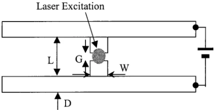
and encapsulation. The ion implantation depth was estimated to be about 100 nm by secondary ion mass spectroscopy measurement. For simplicity, samples implanted with ions of two energies are referred to as multi-GaAs:As⫹, while we refer to single-GaAs:As⫹for samples implanted with ions of one energy. The structure of the photoconductive dipole an-tenna is shown in Fig. 1. The anan-tenna length L, width W, photoconductive gap G, and transmission linewidth D are 10, 20, 5, and 20m, respectively. The experimental setup was a PC emitter–detector system similar to that reported in Ref. 1. The detector was a PC dipole antenna fabricated on a LT GaAs substrate 共grown by the molecular beam epitaxy at 250 °C and annealed at 600 °C for 5 min after the growth兲, whose dimensions were L⫽20m, W⫽10m, G⫽5m, and D⫽5m. The carrier lifetime was estimated to be 0.3
a兲Author to whom correspondence should be addressed; electronic mail: [email protected]
2996
0021-8979/2003/93(5)/2996/6/$20.00 © 2003 American Institute of Physics
ps by a transient photoreflectance measurement. Pumping source for the emitter and receiver antenna was a mode-locked Ti:sapphire laser, which produced 80 fs light pulses at a wavelength of 780 nm and a repetition rate of 82 MHz. A Si hemispherical substrate lens was used for the receiver an-tenna, while no lens was used for the emitter antennas. Irra-diated average power and applied voltage were varied from 0 to about 30 mW and 30 V, respectively. Probe beam power was around 2.5 mW. Figure 2 shows the current–voltage (I – V) curves measured for 20m gaps of multi-GaAs:As⫹ 共ion energies of 150 and 200 keV兲 and single-GaAs:As⫹共ion
energy of 200 keV兲 with the furnace annealing, and also for the same gap of SI GaAs. The dark current characteristic of the SI GaAs, multi-共ion energies of 150 and 200 keV兲, single-ion implanted GaAs共ion energy of 200 keV兲 are com-pared in Table I. Samples used in these measurements had coplanar waveguide type electrodes, and were applied with bias voltages of 30 and 60 V. The annealing process reduced the dark currents of the ion-implanted GaAs to a level共less than or equal to 0.5 nA at a bias of 30 V兲, which was much lower than that of SI GaAs. After annealing, the carrier trans-port mechanism was changed from hopping conduction to thermal emission, corresponding to the reduction in the trap-ping site density.11The antisite defect density was reported to be reduced to about 2 orders of magnitude lower than that of as-implanted materials.12The high resistivity after annealing is attributed to the formation of arsenic precipitates, which is accompanied by recovery of crystallinity and hence an in-crease of the carrier mobility. The dark I – V characteristics
of the single-, multi-GaAs:As⫹ samples were similar, al-though the dark current of the multi-GaAs:As⫹ was slightly lower than that of the single-GaAs:As⫹. The more uniform distributions of arsenic precipitation in the multi-GaAs:As⫹ sample might be better for the high resistivity. Such a low dark current level in the high bias region implies that the multi, or single ion-implanted GaAs can sustain much higher bias electric field than SI GaAs, and thus can increase the emission efficiency of THz radiation.
III. RESULTS AND DISCUSSIONS A. Wave forms and spectra
The THz wave forms emitted from the multi-GaAs:As⫹ 共solid curve兲 and the SI GaAs 共dash curve兲 dipole antenna are shown in Fig. 3共a兲. The applied bias voltage and pumping power were about 10 V and 5 mW, respectively. The wave form of the multi-GaAs:As⫹ antenna was normalized at the main peak amplitude in the wave form of the SI GaAs an-tenna. We observe a clear difference between the two wave forms: the minimum peak after the main peak is sharper and bigger than that for the SI GaAs antenna, while the minimum peak before the main peak decreased compared to that of the SI GaAs antenna. Reflecting this difference, the Fourier transformed spectrum of the wave form for the multi-GaAs:As⫹ antenna is shifted to a higher frequency region compared to that of the SI GaAs antenna 关Fig. 3共b兲兴: The frequency at the spectrum peak for the GaAs:As⫹antenna is 0.9 THz, while it is 0.7 THz for the SI GaAs antenna, and the full width at half maximum共FWHM兲 bandwidth of the spec-trum distribution is about 1.2 THz. To explain the observed difference in the wave forms of the THz radiation emitted from the two antennas, we need to consider the carrier dy-namics in each photoconductive substrate.
In order to interpret the THz radiation wave form, we use the dipole radiation approximation, where the emitted field is assumed to be proportional to the time derivative of the transient current J(t) at far field: ETHz(t)⬀J(t)/t. In
this approximation the main共positive兲 peak observed in the wave forms in Fig. 3共a兲 is attributed to the rises of the surge current by the photocarrier injection and the subsequent car-rier acceleration under the bias field in the PC antennas, while the second negative peak preceded by the main peak is attributed to the decay of the current governed by the carrier trapping times. The origin of the first negative peak before the main peak is attributed to the pulse reshaping effect due
FIG. 2. Electrical characterization of GaAs:As⫹and SI GaAs by I – V mea-surement.
TABLE I. Comparison of dark current between SI-GaAs, multi- and single-ion implanted GaAs.
SI GaAs Multi-implant GaAs Single implant anneal 30 min Single implant anneal 60 min Multi-implant anneal 30 min Multi-implant anneal 60 min Bias 30 V 18 nA 3.83A 0.05 nA 0.13 nA 0.29 nA 0.52 nA Bias 60 V Breakdown Breakdown 0.15 nA 0.28 nA 1.2 nA 1.7 nA
FIG. 1. Schematic diagram of the PC antenna.
2997 J. Appl. Phys., Vol. 93, No. 5, 1 March 2003 Liu, Tani, and Pan
to the frequency dependent THz beam focus on the detector antenna, which gives rise to an equivalent effect of a high-pass filter to the THz radiation.14,15
For the GaAs:As⫹antenna, we have to consider the car-rier dynamics in the ion implanted layer and also in the SI GaAs substrate layer beneath because the optical penetration depth 共⬃1 m兲 of the infrared laser light is larger than the ion implanted layer 共⬃100 nm兲 and, hence, a significant amount of carriers are excited in the SI GaAs layer. If the pump laser pulse width (␦t) is larger than the carrier
mo-mentum relaxation time (m), and if the carrier lifetime (c) is larger than the pump laser pulse width (m⬍␦t⬍c), the current rise is determined by the pump laser pulse width. This is exactly the situation in our experimental condition, where the momentum relaxation time was estimated to be about 30 fs, the laser pulse width was 80 fs, and the carrier lifetime was⬃0.3 ps 共in the ion implanted layer兲 or ⬎100 ps 共in the SI GaAs layer兲, respectively. Therefore, the carriers in both layers contribute to the current rise in the same way after the excitation in the GaAs:As⫹ antenna. However, be-cause the carrier decay time in the ion-implanted layer is shorter than that in the SI GaAs layer, the carriers in the SI GaAs layer are blocked by the ion-implanted layer, which returns the original insulating state after the fast carrier de-cay. Therefore, we can conclude that the transient current in
the GaAs:As⫹ antenna is governed by the carrier dynamics in the ion implanted layer. This model explains the sharp negative peak after the main peak共and the resultant spectrum shift to the higher frequency side兲, which is attributed to the fast current decay in the ion implanted layer.
Figures 4共a兲 and 4共b兲 show the THz radiation wave forms and spectrums for the SI GaAs dipole antenna at vari-ous bias voltages 共1, 5, 10, 15, and 20 V兲. The wave forms were normalized at their main peak amplitudes. The main peak amplitude increased linearly with the bias voltage, and the second negative peak amplitude changed nonlinearly de-pending on the bias. The inset in Fig. 4共a兲 shows the bias dependence of the amplitude at the negative peak. In addi-tion, we can see that the positive main peak shifts slightly to the earlier time delay with the increase in bias. Similar be-havior was also observed for the case of multi-GaAs:As⫹as
FIG. 3.共a兲 THz radiation pulses from small gap 共5m order兲 photoconduc-tive antenna fabricated on multi-implant GaAs:As⫹ 共solid curve兲 and SI GaAs共dashed curve兲. 共b兲 Fourier-transformed amplitude spectrum of 共a兲.
FIG. 4. 共Color兲 Bias dependent THz radiation 共a兲 wave form and 共b兲 spec-trum of SI GaAs fabricated PC antenna with pumping power of 10 mW.
shown in Fig. 5共a兲, although the relative change in the sec-ond negative peak was much smaller关The inset in upper part of Fig. 5共a兲 shows the bias dependence of the amplitude at the negative peak.兴 The spectral peak was shifted from 0.7 to 0.9 THz for the SI GaAs antenna when the bias was in-creased from 5 to 20 V as shown in Fig. 4共b兲. On the other hand, there was no significant change in the center frequency 共⬃0.9 THz兲 for the GaAs:As⫹antenna as shown in Fig. 5共b兲.
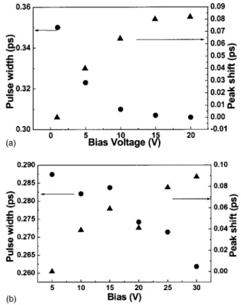
Bandwidth was also broadened significantly in the case of SI GaAs with the increase of the bias, while the bandwidth change for the GaAs:As⫹ was slight. These features are clearly shown in Fig. 6, where the bias dependent pulse width of the main peak 共FWHM兲 and the time shift of the peak position were plotted for the SI GaAs antenna 关Fig. 6共a兲兴 and the GaAs:As⫹ antenna关Fig. 6共b兲兴.
The phenomena of increasing amplitude at the negative peak and the shift of the wave form to earlier time delay is explained by the scattering of photoexcited electrons from the high mobility⌫ valley to the low-mobility L valley under the bias field, as was explained for the case of LT GaAs PC antennas in Ref. 16. The higher the bias field, the faster the acceleration and scattering of electrons to the L valley, re-sulting in the wave form shift to the earlier time delay and more efficient deceleration of electrons共which gives rise to a larger negative peak amplitude in the wave form兲. This in-tervalley scattering effect is expected to be more significant in SI GaAs because of the longer carrier lifetime, while the carriers in the ion implanted GaAs could not have enough time to be scattered to the L valley because of the short carrier lifetime共⬃0.3 ps兲.
B. Emission efficiency
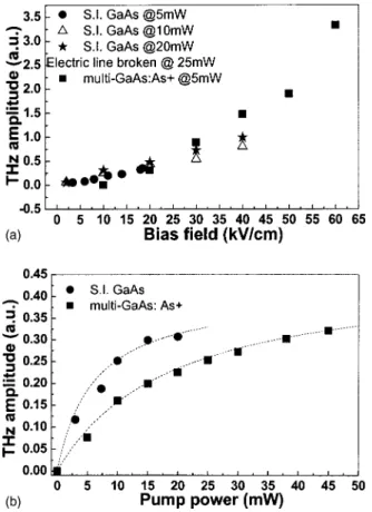
Figure 7共a兲 shows the bias field dependence of the peak amplitude of THz wave form for the 5 mm gap photocon-ductive antennas on SI GaAs and GaAs:As⫹with a pumping power of 5 mW. The GaAs:As⫹ antenna showed a higher breakdown voltage threshold 共⬎60 kV/cm兲 than for the SI GaAs antenna 共⬍45 kV/cm兲. The higher breakdown voltage is an advantage of GaAs:As⫹antennas against SI GaAs since a higher bias means a better THz radiation emission effi-ciency. Beyond 25 kV/cm bias field, THz radiation amplitude emitted from the GaAs:As⫹ antenna was larger than that of the SI GaAs antenna with a pump power of 20 mW even though the pump power for the GaAs:As⫹antenna was only 5 mW.
FIG. 5. 共Color兲 Bias dependent THz radiation 共a兲 wave form and 共b兲 spec-trum of multi-GaAs:As⫹fabricated PC antenna with pumping power of 10 mW.
FIG. 6. Pulse width and peak shift of THz radiation from:共a兲 SI GaAs and
共b兲 multi-GaAs:As⫹fabricated PC antenna as a function of bias voltage as
extracted from Fig. 5.
2999 J. Appl. Phys., Vol. 93, No. 5, 1 March 2003 Liu, Tani, and Pan
Figure 7共b兲 shows the pump power dependence of the peak amplitude in the THz wave form for the SI GaAs and GaAs:As⫹ antennas under a constant bias voltage of 5 V. The amplitude of the emitted THz radiation from the SI GaAs antenna was much higher than the GaAs:As⫹antennas at exciting powers below 20 mW. The high efficiency of SI GaAs antennas at low excitation powers can be explained by the higher photoconductive gain due to the long carrier life-time and a higher mobility than those of GaAs:As⫹. How-ever, the THz signal from the SI GaAs antenna saturates around 15 mW and decreases beyond 20 mW. On the other hand, the THz signal from the GaAs:As⫹antenna increased almost linearly up to 45 mW共the highest power used in this experiment兲 and exceeded the signal from the SI GaAs an-tenna. The saturation properties due to the carrier-screening effects were discussed by Benicewixz et al.,17 and Darrow
et al.18 for large-aperture PC antennas. The same discussion can also be applied to the case of small gap PC antennas by taking into account the effect of the nonuniform spatial ra-diation pattern of a dipole antenna, which only gives rise to a difference by a constant factor in the radiation emission efficiency.2The saturation behavior of THz radiation ampli-tude Er against the pump intensity F or pump power P can be expressed as Er⬀ F/F0 1⫹F/F0 ⫽ P/ P0 1⫹P/P0 , 共1兲
where F0 and P0 are the characteristic saturation intensity
and saturation power for the PC antenna, which depend on the carrier mobility in the PC material. Theoretical curves fitted to the experimental data for these two PC antennas are shown in Fig. 7共b兲 by dashed lines. The agreements between the theoretical curves and the experimental results are very good in both cases. The characteristic saturation intensity P0
for GaAs:As⫹ 共⬃20 mW兲 is much higher than that of SI GaAs 共⬃6 mW兲, and similar to that of LT GaAs.1 Because the saturation power is proportional to the inverse of the carrier mobility,17 we can estimate the relative mobility of GaAs:As⫹ to that of SI GaAs. If we assume the electron mobility of SI GaAs is about 5000 cm2/V s, the effective carrier mobility for GaAs:As⫹ substrate is estimated to be about 1500 cm2/V s. When we take into account the fact that the carriers excited in the layer of the As ion implanted re-gion is only about 10% of the total carriers, while others are excited in the SI GaAs substrate region, the value of carrier mobility in the As ion rich layer is estimated to be about 150 cm2/V s, which is comparable to the reported value of mo-bility in LT GaAs共⬃200 cm2/V s兲.2
IV. CONCLUSIONS
In summary, we showed that the THz radiation wave forms of ion-implanted GaAs:As⫹PC antennas were bipolar and exhibited a sharper and deeper negative second peak than in the case of the SI GaAs antenna. We attributed this wave form characteristic to the ultrafast carrier decay in GaAs:As⫹. Bias dependent wave forms of the GaAs:As⫹ and SI GaAs antennas were explained by the L-valley scat-tering of electrons, which should have been less significant for the GaAs:As⫹due to the short carrier lifetime. The bipo-lar wave form of the GaAs:As⫹antennas resulted in a spec-tral distribution shifted to a higher frequency. Other advan-tages of the GaAs:As⫹ based PC antenna are the high damage threshold biasing 共⬎60 kV/cm兲 and the large satu-rating optical pumping power共⬃20 mW兲 compared to those of the SI GaAs based antennas 共bias ⬍45 kV/cm and satu-ration power ⬃6 mW兲. From the relative saturation depen-dence on the pump power to that of the SI GaAs antenna, the carrier mobility in the As ion implanted layer of GaAs:As⫹ was estimated, including the SI GaAs substrate effect, to be about 150 cm2/V s, which was comparable to that of LT GaAs. However, the emission efficiency might be better compared to LT GaAs based antennas because of the higher effective mobility of 1500 cm2/V s in GaAs:As⫹/SI GaAs substrate. With the higher bias field and larger pumping power confirmed in this study, GaAs:As⫹is promising as the substrate of the PC emitter antennas for THz radiation.
ACKNOWLEDGMENT
T.-A.L. and C.-L.P. acknowledge the support from the National Science Council of the Republic of China under various grants.
1M. Tani, S. Matsuura, K. Sakai, and S. Nakashima, Appl. Opt. 36, 7853
共1997兲.
2
M. Tani, K. Sakai, and H. Mimura, Jpn. J. Appl. Phys., Part 2 36, L1175
共1997兲.
3F. W. Smith et al., Appl. Phys. Lett. 54, 890共1989兲. FIG. 7.共a兲 Bias field and 共b兲 pumping power dependencies of THz radiation
amplitude for 5m gap size PC antenna based on SI GaAs and GaAs:As⫹ with pumping power of 5–20 mW and bias voltage of 5 V.
4D. C. Look, Thin Solid Films 231, 61共1993兲. 5
C. Ludwig and J. Kuhl, Appl. Phys. Lett. 69, 1194共1996兲. 6S. Kono, M. Tani, and K. Sakai, Appl. Phys. Lett. 79, 898共2001兲. 7F. Ganikhanov, G. R. Lin, W. C. Chen, C. S. Chang, and C. L. Pan, Appl.
Phys. Lett. 67, 3465共1995兲. 8
G. R. Lin, W. C. Chen, F. Ganikhanov, C. S. Chang, and C. L. Pan, Appl. Phys. Lett. 69, 996共1996兲.
9A. Claverie, F. Namavar, and Z. Liloental-Weber, Appl. Phys. Lett. 62, 1271共1993兲.
10M. Lambsdroff, J. Kuhl, J. Rosenzweig, A. Axmann, and J. Schneider, Appl. Phys. Lett. 58, 1881共1991兲.
11G. R. Lin, W. C. Chen, C. S. Chang, S. C. Chao, K. H. Wu, T. M. Hsu, W.
C. Lee, and C. L. Pan, IEEE J. Quantum Electron. 34, 1740共1998兲. 12G. R. Lin and C. L. Pan, Appl. Phys. B: Lasers Opt. 72, 151共2001兲. 13G. R. Lin and C. L. Pan, Opt. Quantum Electron. 32, 553共2000兲. 14
C. Fattinger and D. Grischkowsky, Appl. Phys. Lett. 54, 490共1989兲. 15P. U. Jepsen, R. H. Jacobsen, and S. R. Keiding, J. Opt. Soc. Am. B 13,
2424共1996兲. 16
C. Ludwig and J. Kuhl, Appl. Phys. Lett. 69, 1194共1996兲.
17P. K. Benicewicz, J. P. Roberts, and A. J. Taylor, J. Opt. Soc. Am. B 11, 2533共1994兲.
18J. T. Darrow, X.-C. Zhang, and D. H. Auston, Appl. Phys. Lett. 58, 25
共1991兲.
3001
J. Appl. Phys., Vol. 93, No. 5, 1 March 2003 Liu, Tani, and Pan