1
國立交通大學
電子工程學系 電子研究所碩士班
碩 士 論 文
以奈米壓印技術製作大面積次微米孔洞陣列
Development of a nano imprint process for
fabricating submicron dot array in large area
研究生: 周智超
指導教授: 崔秉鉞 博士
2
以奈米壓印技術製作大面積次微米孔洞陣列
Development of a nano imprint process for fabricating
submicron dot array in large area
研 究 生:周智超 Student: Chih-Chao Chou
指導教授:崔秉鉞 博士 Advisor: Dr. Bing-Yue Tsui
A Thesis
Submitted to Department of Electronics Engineering and Institute of Electronics College of Electrical Engineering and Computer Science
National Chiao Tung University in partial Fulfillment of the Requirements
for the Degree of Master
in
Electronics Engineering 2011
Hsinchu, Taiwan, Republic of China
i
以奈米壓印技術製作大面積次微米孔洞陣列
研究生:周智超 導教授:崔秉鉞 博士
國立交通大學
電子工程學系 電子研究所碩士班
摘
要
薄膜太陽能電池是值得期待的下世代太陽能電池之一,理因其低廉的價格和多 方面的基板應用。多年研究下已研發出許多方法可以製作薄膜太陽能電池,
empty-space in silicon (ESS) 是其中可期待的方法之一。 ESS 的優勢在於製程上
的低花費並能提供了良好的能量轉換率。然而,如果能夠導入奈米壓印技術取代 原本的深紫外線的微影製程會是一個更大的突破。 "軟性"奈米壓印改良自原本的奈米壓印,以軟性的圖章取代傳統的硬式材質, 因此有更好的延展和耐用性並能達到高解析度和良好的均勻度。除此之外,軟性 奈米壓印並有機會在高低落差較大的試片上展現良好的性能。軟性奈米壓印可以 解析為下列三種步驟:(1)製作軟性圖章 (2)壓印步驟 (3)圖形轉換。首先為了證 明此技術在量產上有其優勢,我們比較了此技術和目前主要的下世代微影技術,
並以 cost of ownership (CoO)模型來證明軟性奈米壓印的可行性。
在製作軟性圖章上,一個適合的硬質罩幕層是影響表現的重要條件之一。不理
想的幕層設計會導致圖形的變形和崩解。在此,我們考慮了變形的模型進而設計
ii 驟中,抗黏層的塗佈有相對性的重大影響。實驗的過程中,我們並發現要達到均 勻的表面並能保持較高的光阻高度差必須考量到適當的光阻塗佈厚度。由於奈米 壓印的基本原理來自於光阻的流動和空洞的填補。在此概念下,成功發展出一個 簡易的計算求出最恰當的光阻塗佈厚度,並且藉此達到良好的壓印成果。 在壓印的圖形上會有一層多餘的光阻層需要去除以達到後續良好的蝕刻圖形, 在此我們以氧氣電漿蝕刻的方法與之去除,此法不僅簡單更有顯著的效果。而後 續矽的蝕刻則以SF6 混合O2來進行研究。本文中討論了蝕刻製程中幾個重要的條 件,例如壓力,氣體流量和能量功率。在氧氣的濃度增加的情況下,側壁的保護 相對的提高但也因此減弱了蝕刻的能力。研究中也顯示在低功率和高壓力下,蝕 刻的表現是較好的,無論是在側壁保護或是相對的蝕刻率上。 但也由於製程上的限制,單純以 SF6 混合 O2進行的蝕刻無法達到 ESS 對孔洞 深度的要求。因此,我們刻意蝕刻出倒金字塔形狀的孔洞結合陽極氧化的步驟達 到極深的孔洞。但又考量到此條件下的孔洞,其直徑的變異太大可能會增加 ESS 的困難度。因此,我們在矽晶片上沉積了一百奈米的二氧化矽當作額外的硬質罩 幕層,而成功的製作出符合 ESS 要求的周期性孔洞。最後,實驗的結果客觀地 顯示出軟性奈米壓印有著其多樣的發展性,且能在低花費且快速的情況下完成。
iii
Development of a nano imprint process for fabricating
submicron dot array in large area
Student:Chih-Chao Chou Advisor:Dr. Bing-Yue Tsui
Department of Electronics Engineering and Institute of Electronics
National Chiao Tung University
Abstract
Thin-film solar cells are one of the promising approaches for the next generation of solar cells among various approaches due to their low price and wide applications of different substrates. There are many techniques to achieve thin-film solar cells. A layer-transfer process based on the empty-space in silicon (ESS) technique has a promising opportunity, because it presents potentially a better tradeoff between energy conversion efficiency and cost than other techniques. However, its biggest challenge is to reach competitive prices. The development of nano imprint lithography (NIL) as an alternative to optical lithography such as deep-ultra-violet (DUV) lithography is an important aspect of decreasing the cost.
Soft-NIL is an improved technique providing a high-resolution and good uniformity patterns by using a soft stamp instead of a rigid stamp. The soft-NIL process is briefly composed of the following three steps: (1) Fabrication of soft stamp, (2) imprint process and (3) pattern transfer. Here, we compare soft-NIL with other possible next generation lithography, and use the model called cost of ownership (CoO) to prove the feasibility of soft-NIL.
For the fabrication of the soft stamp, a suitable hard mask as a mold for soft stamp is the most important factor that affects the performance. Inappropriate design of the hard mask will result in deformations such as buckling, lateral collapse, and roof
iv
collapse. After considering deformation models, we fabricate soft stamps avoiding the above deformations. Besides, the soft stamp is proved sufficiently stable and reusable even over ten times imprint.
Concerning the imprint process, an anti stick layer coating strongly affect the performances, and the findings for imprinting a uniform structure and high resist contrast over a large area by calculating a suitable polymer thickness are demonstrated. Based on the optimized concerns including squeeze flow and cavity-filling mechanisms, we successfully imprint uniform structures with very thin residual layers over a large area.
Oxygen plasma is used to remove the residual layer, and anisotropic etching of silicon is performed by SF6 and O2 plasma. We prove the importance of accurately
removing residual layers, and the essential of uniform imprinted structures. We report detailed discussions of the link between the etching profiles and etch parameters such as power, pressure, and gas flow. When higher O2 concentrations are added, it causes
a better sidewall passivation but also decreases the etching rate of silicon. Therefore, improvements of the anisotropic etching are shown by applying low power density and high pressure since low power density strongly decreases the lateral etching and high pressure increases the silicon-etching rate.
Extremely deep pores achieved are achieved owning to a combination between dry-etch and anodization, because the soft-NIL patterning process allows to make regular pores. A better control of anodization is performed by an inverted-pyramid-shaped cavity intentionally etched providing specific points to etch. Based on this thought, we take advantage on a negative effect existing in dry etching process, which results in slopped sidewalls.
In the end, we deposit 100 nm silicon oxides before coating the thermal resist, and use this oxide as mask to etch silicon for the desired structures. The imprinted structures show the same property when imprinting above silicon oxide. Therefore, we could fabricate desire structures based on proper etching conditions in this process, and the results show many possibilities of soft-NIL.
v
Acknowledgements
I got help from many people, and I could not have finished this thesis without them. A Taiwanese writer said, “Because of the need to thank so many people, just thank the sky”. However, I still want to say something to show my sincere gratitude.
Primarily, I would like to express my sincere thanks to Prof. B. Y. Tsui, he encouraged me to study abroad and reminded me focusing on the original knowledge of research during my graduation life. Thanks are extended to F. S. Yeh, Prof. H. C. Cheng and Prof. Y. T. Cheng for attending my presentation and for their time and expertise to evaluate my thesis.
Moreover, I would like to thank my promoter, Prof. Dr. J. Poortmans, and our group leader, Dr. Ivan Gordon in IMEC last year. They gave me the opportunity to participate in this project, and work in this top research institute “IMEC”. Besides, their valuable guidance and encouragement kept me improving personally and professionally. Thanks are also extended to Prof. Dr. P. Heremans and Prof. Dr. J. P. Celis for being my committee members and for their time and expertise to evaluate my thesis.
I would also like to thank my supervisors, Dr. David Cheyns and Dr. Valerie Depauw. I would like to thank David for training me in imprinting technique, and he inspired me greatly during my entire work. When I ask him questions, he always answered me at his best and gave me more feedback than I expected. I would also like to express my sincere thanks to Valerie who was always available to me for any research related discussion, no matter how busy she was. She acted as a perfect supervisor who never gave me any stress, and shared her profound knowledge as much as she could. Therefore, I learned a lot and found lots of fun in my work. During this year, I always told myself I am a lucky person to have these two supervisors. It is hard to express my fully thank for them only by writing. Without help of the particular that mentioned above, I would face many difficulties while writing this thesis. Besides, I would like to thank some other people who helped me
vi
finish this work. Izabela and Dries for their help with the SEM, and Cédric Rolin for his kind help with the AFM. Special thanks to Danielle for her willingness to share her experience in fabricating soft stamp. Besides, appreciate to Y. Y. and Kris who characterized the mechanical property. I would like to express my sincere thanks to all the people who helped me in my success here in IMEC.
Due to the extra experiments done in the NCTU, I have to thank the people who help me to finish the experiment in Taiwan. I would like to express my sincere thanks to Prof. F. S. Yeh and her student N. H. Chen for their kind help about the NIL machines in NTHU. Besides, I got lots of assistance from NFC and NDL, I appreciate all the people who work in these both top research centers in Taiwan. Special thanks to my colleagues in my lab for all the things.
Finally, an honorable mention goes to my friends and family for their understanding and support. I clearly remember those days we had fun together and I could not image how dull and difficult my life would be without yours. I would like to acknowledge the love of my family for their support and encouragement during my school days. They educate me but ask nothing in return. I would also like to express my sincere thanks to my girlfriend who has been standing by my side for these years.
周智超 2010 年
vii
Table of contents
摘 要 ... i Abstract ………iii Acknowledgements ...vTable of contents... vii
List of figures and tables ... ix
List of abbreviations ... xiv
Chapter 1: Introduction ... 1
1.1 Solar cells ... 1
1.1.1 Thin-film solar cells (TFSC) ... 2
1.1.2 Decreasing the cost of the epi-free method ... 3
1.2 Possible solutions for low-cost lithography ... 4
1.2.1 Self-assembly process ... 4
1.2.2 Nano imprint lithography (NIL) ... 5
1.3 Overview and the competitiveness of NIL ... 6
1.3.1 The concept of NIL ... 6
1.3.2 Improved NIL: Soft nano imprint lithography (soft-NIL) ... 8
1.3.3 General comparisons with conventional fine feature lithography ... 8
1.3.4 The calculations of cost of ownership (CoO) ... 10
1.4 Thesis outline ... 13
Chapter 2: Soft Nano imprint lithography ... 18
2.1 Fabrication of soft stamp ... 18
2.1.1 Hard mask ... 18
2.1.2 Soft stamp (PDMS) ... 20
2.2 Imprint process ... 21
2.2.1 Spin coating of the resist ... 21
2.2.2 Imprint ... 22
2.3 Pattern transfer ... 23
2.3.1 Residual layer remove ... 23
viii
2.3.3 Anodization for deeper pores ... 26
2.4 Characterizations of the soft stamp ... 27
2.4.1 Visual inspections... 28
2.4.2 Topography measurements ... 28
Chapter 3: Results and discussion ... 36
3.1 Imprint from hard mask composed of deep pores ... 36
3.1.1 Process with coating anti stick layer ... 36
3.1.2 Process without coating anti stick layer ... 37
3.1.3 Modeling the imprint Deformations ... 38
3.2 Imprint from hard mask composed of shallow pore ... 40
3.2.1 The performance of different thickness of resist... 41
3.2.2 Optimizations of the soft-NIL process ... 42
3.3 The results of Pattern transfer ... 44
3.3.1 Etching silicon without sidewall passivation... 44
3.3.2 Optimization of the residual layer removed by O2 plasma ... 45
3.3.3 Etching Silicon with sidewall passivation ... 46
3.3.4 Influence of different dry-etch parameters ... 47
3.3.5 Fabricate inverted pyramid pre-patterned structures by dry etching ... 48
3.3.6 Anodization process ... 48
3.4.1 Open silicon window ... 50
3.4.2 Etch silicon into desired features ... 51
Chapter 4: Conclusion and Perspectives ... 73
4.1 Conclusion ... 73
4.2 Perspectives ... 74
Bibliography ... 77
ix
List of figures and tables
Figure 1. 1: Schematic illustration of self-organizing sequences for the formation of ESS having three typical structures: (a) sphere, (b) pipe, and (c) plate. The surface layer (c) above the empty-space is potentially detachable [1-6]. ... 15 Figure 1. 2: Process flow of epi-free technique [1-7]. (1): Formation of regular
macropores by DUV lithography combined with a dry etching process. (2): Annealing of these pores for formation of a detachable and singlecrystalline thin film. (3): Solar-cell processing of the first side of the film. (4): Bonding and detachment. (5): Processing of the second side. ... 15 Figure 1. 3: Parameters in porous structure are pore diameter (d), pore wall thickness (w), aspect ratio, and length (l) [1-7]. ... 16 Figure 1. 4: Process flow of nano imprint lithography. ... 16 Figure 1.5: Temperature and pressure cycle of NIL. ... 17 Figure 1.6: Master silicon can be replicated hundreds of times using a soft stamp to imprint. ... 17
Table 1. 1: NIL compared with EBL, AFML, and photolithography. ... 10 Table 1.2: The CoO comparison of soft-NIL and DUV lithography. (Pw=$7, D=5
years, EM= 5% of E0 and U= 70 %) ... 13
Figure 2.1: Experimental flow of soft-NIL, which is composed of soft stamp fabrication in the step 1, imprint process in the step 2 and 3, and the pattern transfer in the step 4 and 5. ... 30 Figure 2 2: The fabrication of the porous structure by DUV lithography and dry
etching [1-7]. ... 30 Figure 2. 3: Two silicon structures used as hard masks. The left one is composed of
440 nm diameter and 700 nm deep pores. The right one is composed of 460 nm diameter and 220 nm deep pores. ... 31 Figure 2.4: SEM image of samples which is acted as hard mask, and the circles are
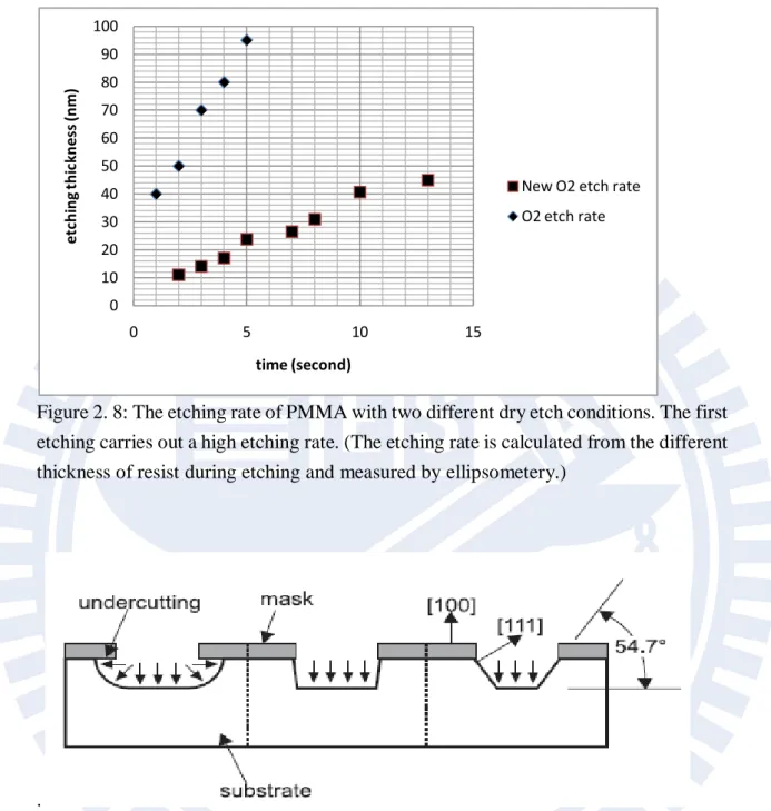
composed of 450 nm diameter. ... 31 Figure 2. 5Teflon container (left) and stainless steel mold (right) used to fabricate the soft stamp. ... 32 Figure 2.6: Schematics of the imprint process (left) [2-2] and the temperature/pressure cycle (right). ... 32 Figure 2. 7: Process flow of pattern transfer. ... 32 Figure 2. 8: The etching rate of PMMA with two different dry etch conditions. The first etching carries out a high etching rate. (The etching rate is calculated from
x
the different thickness of resist during etching and measured by ellipsometery.) ... 33 Figure 2. 9: Overview of (left) isotropic and (middle, right) anisotropic etching.
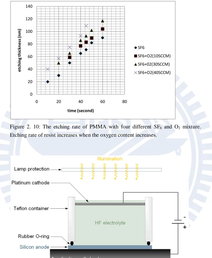
Anisotropic etching by (middle) dry etching or by (right) wet anisotropic etching [2-3]. ... 33 Figure 2. 10: The etching rate of PMMA with four different SF6 and O2 mixture.
Etching rate of resist increases when the oxygen content increases. ... 34 Figure 2. 11: Schematic illustration of an open O-ring anodisation cell. The lamp is a
50-W tungsten-bulb halogen lamp, and the lamp protection is a quartz-glass beaker that protects the lamp from HF vapors [1-7]. ... 34 Figure 2. 12: Left is the result of hard mask from optical profilometer, and we can see a low resolution result. Right is the result of soft stamp from optical profilometer, and we cannot clearly see structures on the surface. ... 35
Table 2. 1: The relation table between resist thickness and spin speed. ... 22 Table 2. 2: The condition of these two O2 recipes ... 24
Figure 3.1: AFM image and depth profile of soft stamp before imprinting with anti-stick layer coating. On average, 400-nm height pillars along line 1. ... 53 Figure 3.2: AFM image and depth profile of soft stamp after imprinting with anti-stick layer coating. On average, 800-nm pitch and 500-nm height pillars along line 1. ... 53 Figure 3.3: AFM image and depth profile of the soft stamp imprinted into 95-nm resist on silicon. On average, 800-nm pitch and 400-nm depth pores along line 1. ... 53 Figure 3.4: SEM image of the soft stamp imprinted into 95-nm-thick resist on silicon. Confirm that etch pillar is closely attached to the adjacent one. ... 54 Figure 3.5: AFM image and depth profile of soft stamp after imprinting without
anti-stick layer coating. On average, 500-nm diameter and 50-nm depth along line 1, and it shows that the pillars do not deform anymore. (The bright spots of the AFM image come from an artificial effect that indicates dirt on the surface of stamp. These particles probably originate from the operating environment.) ... 54 Figure 3.6: AFM image and depth profile of the soft stamp imprinted into 95-nm resist on silicon. On average, 500-nm diameter and 50-nm depth along line 1. 55 Figure 3.7: High-resolution Microscopy image of the soft stamp imprinted into
xi
Figure 3.8: Topography of 3-D image shows the patterns imprinted with a soft stamp composed of (a) 1:5, (b) 1:15 and (c) 1:10 mixture ratio. ... 56 Figure 3.9: Schematic of stamp with width of 2a, height of h, and pitch of 2w [3-5]. 56 Figure 3.10: Three failure modes of stamp deformation. (a) buckling (b) lateral
collapse (c) roof collapse [3-5]. ... 57 Figure 3.11: AFM image and depth profile of soft stamp composed of 500-nm diameter and 230-nm height pillars, and it shows that stamp is perfectly duplicated from the hard mask (Right image of Figure 2.3). ... 57 Figure 3.12: AFM image and depth profile of imprinted structures in 95-nm-thick resist, and the pores are composed of 450-nm diameter and 150-nm depth. .... 57 Figure 3.13: AFM image and depth profile of imprinted structures in 120-nm-thick resist, and the pores are composed of 450-nm diameter and 180-nm depth. .... 58 Figure 3.14: AFM image and depth profile of imprinted structures in 160-nm-thick resist, and the pores are composed of 460-nm diameter and 230-nm depth. .... 58 Figure 3.15: Schematic illustration of the soft stamp. ... 58 Figure 3.16: A schematic representation of squeeze flow of a polymer into a stamp
cavity [3-9]. ... 59 Figure 3.17: Optical microscope image of imprint structure in (a) 250 nm, (b) 160 nm and (c) 95 nm thickness of resist. The best uniformity is obtained in (b) with a 100% cavity fill. ... 59 Figure 3.18: SEM images, from tilted top view and cross section, of an imprinted
structure in 160-nm thickness of resist. There is a uniform topography (left) and a very thin residual layer (right). ... 60 Figure 3.19: High-resolution microscopy images of imprinted silicon etched for (a) 10,
(b) 30, and (c) 40 sec by SF6. The area of the structures becomes larger with increased etching time. ... 60 Figure 3.20: High-resolution microscopy images of imprinted silicon are first etched
by a high etching rate of O2 plasma in one second, and then the silicon etched by SF6 for (a) 10 and (b) 30 seconds. Here, the silicon etching is more effective than without removing residual layer. ... 60 Figure 3.21: SEM images of samples etched by O2 for 1 second and SF6 30 for
seconds. (a) The isotropic etching clearly results in the topography and (b) the large various heights of structures come from the bad uniformity of the imprinted structures. ... 61 Figure 3.22: AFM images of samples etched by O2 for (a) 3, (b) 5 and (c) 8 seconds
and SF6 with 10% O2 for 40 seconds. Showing that 5 seconds is the most appropriate in our experiment. ... 61
xii
Figure 3.23: SEM image of samples etched by O2 for 5 seconds and SF6 with 10% O2 for 40 seconds. Silicon oxide is created on the corners of mesh. ... 62 Figure 3.24: SEM image of samples which is etched by O2 for 5 second and SF6 with 10% O2 for 60 seconds. Disappearance of the structures results from insufficient sidewall passivation. ... 62 Figure 3.25: AFM measurement and SEM images of samples etched by O2 in 5
second and (a) SF6 with 20% O2 for 30 second, (b) 30% O2 for 30 second, (c) 40% O2 for 20 second and (d) 60% O2 for 60 second. ... 63 Figure 3.26: AFM and depth profile of samples etched by O2 in 5 seconds and by SF6 with 40% O2 for (a) 30 seconds, (b) 40 seconds and (c) 70 seconds. ... 64 Figure 3.27: AFM images of samples etched by O2 for 5 seconds and SF6 with (a)
10% O2 and (b) 30 % O2 with pressure of 150 mTorr, power of 150 W for 15 seconds. ... 64 Figure 3.28: AFM images of the sample etched by O2 for 5 seconds and SF6 with
40% O2 with pressure of 200 mTorr, power of 100 W for 60 seconds. ... 65 Figure 3.29: AFM images and depth profile of the sample etched by O2 for 5 seconds and SF6 with 40% O2 with pressure of 300 mTorr, power of 50 W for 180 seconds. The pores with a depth of 450 nm and a diameter of 450 nm. ... 65 Figure 3.30: SEM images of samples etched by O2 for 5 seconds and SF6 with 40%
O2 for 70 seconds. (a) Top view of pre-pattern structures and (b) cross sectional view of inverted pyramid pre-pattern structures... 66 Figure 3.31: SEM image of anodized pores with a current density of 8 mA/cm2 for
300 seconds. (a) Comparison between pre-patterned and bare silicon, (b) cross-sectional view of pre-patterned area and (c) flat area. ... 66 Figure 3.32: SEM image of anodized pores with a current density of 4 mA/cm2 for
240 seconds. (a) Tilted view of pre-patterned area, (b) cross-sectional view of pre-patterned area and (c) cross-sectional view of bare silicon area. ... 67 Figure 3.33: SEM view of anodized pores formed with a current density of 4 mA/cm2 for 240 seconds, from a sample pre-etched with inverted-pyrampids. ... 68 Figure 3.34: Evolution of current during anodization. The set current is 0.1 A, but the irregular current density that is delivered by the generator. ... 68 Figure 3.35: SEM view of pores formed from a sample with inverted-pyramids etched pits anodized with the etching condition of 4 mA/cm2 currnet density for 240 seconds. The backside of the sample was highly doped to obtain a better backside contact. ... 68 Figure 3.36: Experimental flow of soft-NIL, which is composed of soft stamp
fabrication in the step 1, imprint process in the step 2 and 3, the pattern transfer in the step 4 and 5. ... 69
xiii
Figure 3.37: Experimental flow of the pattern transfer. In the first step, use resist as mask to open silicon window, and use silicon oxide as mask to etch silicon in the second step. ... 69 Figure 3.38: SEM image from top view of imprinted structure (left). SEM image from cross section of imprinted structure after removing residual layer (right). ... 70 Figure 3.39: SEM images of samples etched by CHF3 and CF4 with 4 % O2 for open silicon window. (a) The sample is etched for 40 seconds, and the silicon oxides still appear on the bottom. (b) The sample is etched for 60 seconds, and the silicon window is open. ... 70 Figure 3.40: SEM images of samples etched by HBr with Cl2 and HBr with O2. (a)
The sample is etched for 7 and 1 minutes, and the silicon is etched over 1μm. (b) The sample is etched for 9 and 1 minutes, and the silicon is etched over 1.2μm. ... 71 Figure 3.41: SEM images of samples. (a) The sample etched with CF4 and 4 % O2 for 60 seconds. (b) The cross section of sample etched by HBr with Cl2 and HBr with O2 for 11 and 1 minutes after opening silicon window. (c) The top view f sample etched by HBr with Cl2 and HBr with O2 for 11 and 1 minutes after opening silicon window. ... 71 Figure 3.42: SEM images of the sample which is etched by HBr with Cl2 and HBr
with O2 for 13 and 1 minutes, and the silicon oxide is not enough to protect the surface, which appears so rough. ... 72
xiv
List of abbreviations
DUV deep-ultra-violetPV photovoltaic
TFSC thin-film solar cells ESS empty-space in silicon NIL nano imprint lithography
FDTS 1H,1H,2H,2H ferfluorodecyltrichlorosilane EBL electron beam lithography
AFML atomic force microscope lithography PDMS polydimethylsiloxane
Soft-NIL soft nano imprint lithography CoO Cost of Ownership
WPH wafers per hour WPM wafers per mask ARC antireflective coating UV ultraviolet
PMMA polymethylmethacrylate Tg glass transition temperature SCR space charge region
SEM scanning electron microscope AFM atomic force microscope
1
Chapter 1: Introduction
Thin-film solar cells are one of the promising candidates for the next generation of solar cells among various approaches. There are many techniques to achieve thin-film solar cells, and layer-transfer processes have a promising opportunity. An epi-free method combined with reorganization of macro pores is one of these layer-transfer methods. However, the epi-free process involves optical lithography, which is still an expensive and time-consuming step. If we can replace this step by another advanced lithography process, it will save a significant amount of energy and cost. Various alternative lithography techniques are under development and, among the various approaches, nano imprint lithography reveals a higher potential than others to replace the conventional optical lithography. The different points will be discussed in this introduction chapter.
1.1 Solar cells
Developing green energies, which come from natural resources such as sunlight, rain, wind, tides and geothermal heat, is one of the best ways making the environment better. Compared to conventional energies, green energies are cleaner, and renewable unlike fossil fuels which keep harming ther world. Moreover, oil prices reach records year by year, and will definitely not depreciate in the future. In other words, we need to focus on sustainable energies to replace fossil fuels. All of the above issues push scientists into developing a new energy, which can be inexhaustible, and affordable.
Solar cells are a promising candidate for green energy, because their energy is directly derived from the sun, which is a long lasting source of energy, available almost everywhere. Utilization of solar energy creates no pollution except in the production and maintenance of solar cells lead to some amount of pollution, and this is the most important advantage that makes it more practical than conventional energy like oil, which will release greenhouses gases into our air when it burns.
2
The mechanism of solar cells can be simply expressed as following. Photons from the sunlight hit the photovoltaic (PV) cells and are absorbed. Then, electrons are released from their atoms, allowing them to flow through the cell to produce electricity. Different cells are connected together in series and encapsulated into modules. Later, these modules can be constructed into an array to provide a larger current and voltage. There are many different types of solar cells, and (multi-)crystalline silicon solar cells are current industry leader. The main reason is that crystalline silicon solar cell can offer higher conversion efficiency, but the high cost of fabricating them is a main issue. As a result, scientists keep focus on researching new kinds of solar cells offering more affordable price. Based on the tradeoff between cost and efficiency, thin-film solar cells are gaining interest.
1.1.1 Thin-film solar cells (TFSC)
Thin-film solar cells (TFSC) are a promising approach to achieve a low price, and can be applied on variety of different substrates. TFSC cover a wide range of technologies, and we will focus on the issue of thin-film crystalline silicon. Except the silicon based TFSC, other two-component (binary) materials attractive for thin-film solar cells are: GaAs, CdTe, Cu2S, Cu2O, InP, Zn3P2, etc, but the scarcity of these
components and even their toxicity limit their developments [1-1,1-2]. The other thin film technologies, organics and dye-sensitised cells present immense impact on the TFSC industry in the future due to their inexpensive processing and flexible applications [1-3, 1-4]. However, silicon based solar cells have their irreplaceable advantages over the other thin film technologies on its abundance of material, non-toxicity and great connection with the current semiconductor industry. Unfortunately, the thickness of this thin crystalline layer cannot easily be obtained from current wafer techniques.
Hence, there are two ways to make a thin crystalline film; one is to directly deposit a crystalline layer on a substrate, and another is to transfer a thin crystalline layer from a thick wafer to a foreign. The first method requires the use of the epitaxy [1-5] that refers to the method of depositing single-crystalline film on a single-crystalline
3
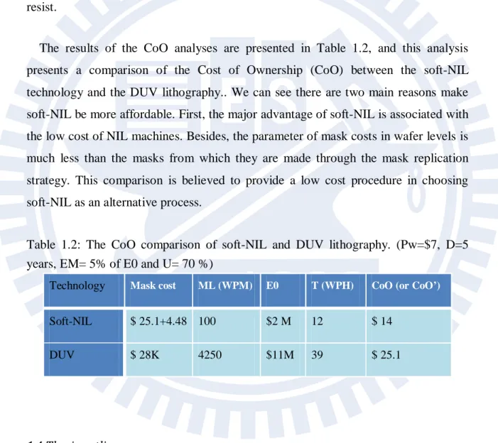
substrate. Although epitaxy is capable of producing high-quality layers, it is low-throughput and high temperature requirements for high-quality layers represent a bottleneck for industrial processes. The latter method, on the other hand, does not require epitaxial deposition and therefore presents potentially a better tradeoff between energy conversion efficiency and cost than the other techniques. A layer transfer process based on the empty-space in silicon (ESS) technique [1-6] would form a high-quality crystalline layer without the step of epitaxy. Therefore, we call this process “Epi-free” method. A plate-shaped ESS below the surface of the silicon can be fabricated by connecting the spherical empty spaces (Figure 1.1-(c)), which are formed by surface migration of Si on the patterned Si substrate upon annealing, and this surface layer above the empty-space is potentially detachable.
1.1.2 Decreasing the cost of the epi-free method
The whole solar-cell process based on the epi-free techniques is composed of the following steps (Figure 1.2). (1): Formation of regular macropores by deep-ultra-violet (DUV) lithography combined a dry etching process. (2): Annealing of these pores for formation of a detachable and singlecrystalline thin film. (3): Solar-cell processing of the first side of the film. (4): Bonding and detachment. (5): Processing of the second side.
Avoiding an expensive process like optical lithography with DUV light as source for forming regular nanostructures is the main idea of this thesis, because the cost of lithography equipment constitutes 25% to 35% of the cost of all semiconductor fabrication equipment [1-8]. DUV lithography equipment costs over $ 10 million, and the cost of lithography equipment has increased at a nearly exponential rate over the past 30 years [1-9]. The limited throughput of DUV lithography is another major disadvantage of this process. If we want to replace it, we need to solve uniformity, resolution and throughput issues. Therefore, I will discuss some possible solutions which are considered as low-cost lithography in the next section (1.2).
4
1.2 Possible solutions for low-cost lithography
Suitable unconventional lithography should meet the epi-free process requirements together with other important issues, so to estimate the feasibility of these possible solutions we base ourselves on the following points. First, the whole process has to be more affordable than the optical lithography like I-line and DUV module, with an acceptable yield. Second, it should have a reliable throughput. Third, it has to meet the requirements on the porous structures that are needed for the epi-free method. The requirements on the porous structures are that these pores can be reorganized to form a thin film. In detail, the important parameters (Figure 1.3) that control the empty-space in silicon are pore diameter (d), pore wall thickness (w), aspect ratio, and length (l). Transformation into a single sphere requires the aspect ratio (l/d) follow the empirical rule between 3 and 9.5, and pore wall thickness should be equal or smaller than the pore diameter [1-10, 1-11, 1-12]. In our expectation, we want to make structure of around 500 nm diameter, and the depth have to be higher than 1.5 µm.
The following section introduces some possible unconventional lithography, and compares them. In the end (1.3), the most appropriate method among them is described.
1.2.1 Self-assembly process
With methods based on self-assembly, disordered components automatically form organized structures from local interactions, without external force like physical contact and optical lithography. Block copolymers, colloidal lithography, and porous alumina are three of those methods of self-assembly that may let us pre-pattern our wafers.
Block copolymers is a technique that uses self-assembling diblock copolymers as nano lithographic masks to create nanostructures [1-13]. In this reference, for example, diblock copolymer micelles were generated in a toluene solution. These micelles were loaded by a noble-metal salt. After dipping a substrate into this solution, a monolayer of ordered micelles is generated, covering almost the complete surface. After treatment in
5
hydrogen plasma, all of the organic components are removed and only crystalline metal clusters of few nanometer sizes remain. This metal cluster mask can be used directly in a chlorine dry etching process. The unsuitable aspect of this process is that it is not possible to achieve deep pores from the very thin resulting mask, and this process only can fabricate around 30 nm deep pores [1-13].
In colloidal lithography, particles can assemble into organized structures in a liquid [1-14]. The hexagonal close-packed motif they form acts as an evaporation mask; with this method planar arrays of diverse nanostructures have been accomplished. Nevertheless, this technology cannot be applicable to cm-large area, and the structure size cannot easily be changed, since it simply mimics the size of the hexagonal close-packed motif [1-15].
Unlike colloidal lithography, porous alumina may be applied to a large area. With this method, ordered pores are used as a template on silicon. In a first step, a layer of aluminum is anodized into porous alumina on the silicon substrate, and etching away the alumina. The next step is to anodize the surface again on certain condition, and the surface will be organized into hexagonal packed arrays. Again, these hexagonal packed can be used as mask to form a structure. [1-16] However, this method is limit by the narrow windows and pitch of the alumina mask.
1.2.2 Nano imprint lithography (NIL)
Nano imprint lithography is a high throughput, low cost, nonconventional lithographic method. It has been listed by MIT’s Technology Review as one of ten emerging technologies [1-17], and the international Technology Roadmap for semiconductor announced the inclusion of NIL on their roadmap as a candidate technology to replace optical lithography [1-18]. The concept of NIL is use a mold with nanostructures to imprint the negative structure on a thin resist on a substrate [1-19].
NIL has demonstrated 25 nm feature size, 100 nm pitch, vertical and smooth sidewalls, and excellent uniformity [1-20], and its applications of 150 mm diameter wafers is also achieved [1-21]. The ultimate resolution of nano imprint can be sub-10
6
nm from further experiment, and paper study [1-22]. Besides, it is also feasible to imprint over a non-flat surface [1-23]. Another advantage of this technique is that the mold is durable, so the imprint process is repeatable. The master mold can be reused multiple times, and as a consequence, the mold itself can be fabricated by a more expensive or more time consuming fabrication method. In addition, the size uniformity area is acceptable if the imprint condition is optimized. Finally, NIL has been successfully in fabricating some nano scale products, and all these advantages push us to research this process as an alternative lithography.
1.3 Overview and the competitiveness of NIL
NIL is a promising method to replace optical lithography in the epi-free method. This section gives an overview of NIL. We will introduce the concept of NIL in 1.3.1, discuss an improved NIL process which is called “soft” nano imprint in 1.3.2, and compare it with conventional fine feature lithography including the calculations of cost of ownership in 1.3.3 and 1.3.4.
The complete process of NIL is composed into following steps (Figure 1.4): (1) Fabrication of the hard mask composed of regular pores by conventional lithography. Pressing this hard mask into the resist which was spin coated on the substrate. (2) Demolding of the hard mask, to duplicate the negative nano structures in the resist. (3) Dry etching to remove the residual layer of resist and etch the substrate. (4) Removal of the remaining resist on the surface.
1.3.1 The concept of NIL
NIL was mentioned for the first time in 1995 in an article by Chou et al. [1-19]. NIL is based on the deformation of a thermoplastic resist coated on the substrate by using a rigid stamp. The work presented in the first article started activities on NIL all around the world. NIL acts as a potential cost-efficient nanofabrication technique and as a way to realize simple devices in a patterning step. Besides, NIL is a promising technique, which allows us to obtain nanometer scale on large size wafers.
7
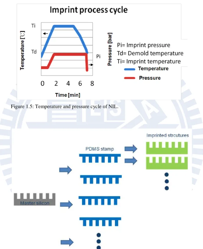
A stamp (hard mask) with the desired nanometer features is needed. This is usually fabricated by, for example, optical lithography or electron-beam lithography combined with dry etching. The resist to be printed, a printable polymer, is spun onto a solid substrate. The stamp and the substrate are placed on parallel stages. These are heated up to the printing temperature, which is above the glass temperature of the polymer to be molded and a certain amount of time is allowed for the thermal equilibrium to be reached. Then, the stamp and resist are brought into physical contact and pressure is applied, followed by subsequent cooling and then demolding. In Figure 1.5, temperature and pressure cycle of NIL is shown. The next step is the pattern transfer where an anisotropic etching process, is used to remove the residual resist and silicon etching in the compressed area.
The estimated imprint cycle for NIL is a few minutes. The imprint time mainly depends on three things the viscosity of the thermoplastic polymer, the stamp protrusion size, and of course the heating and cooling time provided by the NIL machines. It can be concluded that by optimizing the imprint time NIL can become a fast nano lithography tool compared to other lithographies. By patterning a single master stamp for NIL by time expensive lithography techniques and then replicating the master stamp by the NIL technique, NIL becomes a rather fast technique for patterning of features in the nanometer range. An obvious use of the technique would be to make optical devices since these often tend to have some periodicity in the structures, and typically demand sub-wavelength patterns in the order of a few hundred nanometers with a resolution in the order of a few tens of nanometers.
Adhesion is a very important issue in NIL. Consequently, the use of anti stick treatment for stamps containing sub-100 nm features is reported [1-24]. Ideally, the resist should stick to the substrate but not to the stamp, so that the stamp can be safely removed safely after the imprint. For a perfect separation, the substrate should have a large surface energy so that the resist may adhere well to it, while the stamp should have a low surface energy. Specifically when the stamp feature size gets smaller the sticking tendency between polymer and stamp is enhanced, demanding an anti stick layer. Appling anti stick coatings can reduce the adhesion between the two surfaces.
8
Using 1H,1H,2H,2H perfluorodecyltrichlorosilane (FDTS) as anti stick layer to obtain a very low surface energy is presented [1-25]. The resulting silane layer prevents adhesion of the stamp to the surface resist of silicon substrate. Moreover, a low surface energy released layer on the stamp surface not only helps to improve imprint qualities, it also significantly increases the stamp lifetime by preventing surface contamination.
1.3.2 Improved NIL: Soft nano imprint lithography (soft-NIL)
NIL involves applying a high pressure for the imprinting of the patterns into an underlying polymer, and high temperature, which has to be above Tg of the substrate polymer for several minutes. In such conditions, the hard mask like bare silicon or chrome mask supported on a glass plate has a high risk of brittle failure for the mask and the substrate. Therefore, some apparent limitations inherent in the NIL make it somewhat unsuitable for forming high resolution and complex structures, and it is even worse for leading to no pattern formation by using a hard mask [1-28]. Another disadvantage is that this technique is unsuitable in conforming to non-uniform large areas [1-34].
A solution to these problems is the usage of a soft, bendable stamp. This soft material typically is polydimethylsiloxane (PDMS) which has been considered highly effective based on its characteristic of low elastic modulus and low surface energy [1-35]. These properties allow a PDMS stamp to produce consistent nano-scale imprints on the surface of resists, over large contact areas regardless of a substrate’s topographic uniformity by conforming to the surface during contact and yielding during release [1-36]. Moreover, the pressure induced by local irregularities as dust particles will be distributed over the mold, reducing the chance of breaking the substrate [1-37]. Extra care for this technique is to avoid difficulties during the separation of the hard mask from the patterned substrate, but this problem can be solved by coating anti stick layer on the surfaces. Because of these advantages, we developed a soft nano imprint process in this work.
9
To appreciate the potential of NIL, an overview of different modern techniques to produce very fine features discussed in this section: Photolithography, electron beam lithography (EBL), and atomic force microscope lithography (AFML).
Photolithography is based on a projection-printing system in which the image is projected onto a thin film of photoresist that is spin-coated on a wafer through a high numerical aperture lens system. The resolution of the system is subject to the limitations set by optical diffraction according to the Rayleigh Equation [1-26], Resolution=k1λ/NA, where λ is the wavelength of the illuminating light, NA the
numerical aperture of the lens system, and k1 a constant that depends on the photoresist.
As a result, illuminating sources with shorter wavelengths are progressively introduced into photolithography to generate structures with smaller feature sizes. It is plausible that features as small as 100 nm can be manufactured optically by employing advanced mask resist technologies and DUV radiation, and extreme Ultra-Violet (EUV) lithography is being developed for next generation integrated circuits [1-27]. The sizes of the features fabricated by photolithography are limited to optical diffraction, and the high-energy radiation needed for small features requires complex facilities and technologies [1-28]. As structures become increasingly small, they also become increasingly difficult and expensive to produce. These techniques are capable of generating very small features, but the development into practical commercial methods for low-cost processing still requires great ingenuity [1-29].
EBL refers to lithographic process is the practice of scanning a focused electron beam of to form patterns across a surface covered with resists, and of selectively removing either exposed or non-exposed regions of the resist. The primary advantage of EBL is that it can overcome the diffraction limit and the cost of mask fabrication; thus, it allows a small diameter electron beam to be scanned over a surface. However, it takes a very long time including moving the beam across the surface to expose. The writing speed of an electron beam system in wafers can be estimated by considering the total beam current incident on the wafer and the sensitivity of the resist [1-30]. In a contact-printing mode, EBL can reach a writing speed of 0.02 cm2/sec, but its exposure systems are rather complex and expensive [1-31].
10
AFML uses an AFM to oxidize a surface by applying a voltage difference between the tip and the surface [1-32]. The oxidized pattern can subsequently be used as an etch mask to transfer the pattern into the substrate. Applying an AFM it is possible to achieve line widths down to 10 nm and a typical scan speed of the AFM is in the order of 5 μm/sec [1-33]. In the following table, throughput, cost, and resolution of EBL, AFML and photolithography are compared to those of NIL. We can clearly learn the throughput is NIL’s strength compared to other process. More importantly, the low cost consumption of NIL is the driven force to push this process into mass production.
Table 1. 1: NIL compared with EBL, AFML, and photolithography.
Throughput Cost Resolution
NIL High Low High
EBL Low High High
AFML Low Middle High
Photolithography High High High
1.3.4 The calculations of cost of ownership (CoO)
Although the optical lithography is still the mainstream process today, scientists are still searching for replacements that have lower cost with fine features. During the development of such new processes, the cost of ownership (CoO) is a possible analysis for users to estimate the practicability of new processes and understand what modifications are necessary. CoO represents the cost of lithography per wafer level and it is widely used to compare lithography costs of various technology options. An integral CoO of lithography is modeled by International SEMATECH to compare the competing lithography technologies in an unbiased way [1-39].
The basic CoO model which is shown in formula {a} assumes that the cost per wafer level is the sum of process, mask, and tool costs [1-39, 40]. The calculations of this
11
model are determined from the following parameters. Process cost is assigned to the cost of resist and etching process, and this parameter is assumed to be constant as $7 in each calculation [1-41]. Here, we have to notice that this assumption is relatively conservative due to the low resist costs of soft-NIL, and the etch costs are expected to be comparable to that of optical lithography. Besides, there is extra cost of the PDMS (soft stamp), but this material reveals a quite affordable price. Mask usage describes the whole lifetime of single mask during the exposedness. Mask cost is defined as the cost of fabricating the mask including the material and process. The calculations of CoO are predictably reduced in high mask usage and low mask cost. Another key parameter of CoO is the capital equipment cost, which affect the results in a determined way due to its extremely high price in extra-advanced machine. The throughput of the exposure system closely influences the tool cost since the cost of the capital equipment will be reduced over more wafers. Besides, other parameters are assumed constant in all the calculations. First, Lithography equipment annual maintenance costs is always assigned as certain percentage as 5% of capital equipment, and all the equipments will depreciate in 5 years [1-41]. Second, the utilization of the equipment is 70 % no matter of optical lithography or NIL equipment.
CoO = P
w+
MML0+
(D)(T)(U)(365)(24)E0+(D)(EM){a}
Here, Pw = Process cost per wafer level (resist and etch costs).M0 = Mask cost in $.
ML = Mask usage in number of wafer levels.
E0 = Capital equipment costs in $.
EM = Lithography equipment annual maintenance costs in $.
D = Equipment depreciation in years. U = Utilization of equipment.
T = Throughput in wafer levels per hour.
.
T
he strategy of soft-NIL is not as the same as optical lithography, and we can understand the ideas form Fig. 1.6. We use master silicon as hard masks to duplicate numerous PDMS (soft stamp), and use each stamp fabricating imprinted structures. Therefore, we should slightly transform the original formula into a new one which is12
suitable for soft-NIL. In the formula {b}, CoO’ is also the sum of process, mask, and tool costs. It is noticeable that the difference is the mask costs compared to basic CoO, and it comes from the strategy mentioned before. Each master silicon which is fabricated from optical lithography can duplicate numerous imprinted structures. Therefore, the hard mask cost is derived from the CoO in optical lithography and extra etching cost [1-42]. Besides, the mask usage depends on how many imprinted structures can be obtained.
CoO′ = P
w+
CoO+CeML+
(D)(T)(U)(365)(24)E0+(D)(EM){b}
Here, Pw = Process cost per wafer level (resist and etch costs)CoO= Hard mask cost in $ Ce= Etching cost in $
ML = Hard mask usage in number of wafer levels
E0 = Capital equipment costs in $
EM = Capital equipment annual maintenance costs in $
D = Equipment depreciation in years U = Utilization of equipment
T = Throughput in wafer levels per hour
Given the statistics below, the cost per wafer can be calculated based on the formula. First, the mask costs are simplified as the volume selected for the mask shop is 100 masks per week, but are necessary for comparative modeling. Besides, the results indicate the change in mask cost is very small when mask line with run rates of greater than 100 masks per week [1-43, 1-44]. In DUV lithography, the mask cost around $ 28K. Regarding the mask usage, it tends to have higher mask usage in semiconductor industry. For this reason, the mask usage has the range from 500 wafers per mask (WPM) to 8000 WPM [1-41]. Here, we suppose it to be their average as 4250 WPM. For the soft-NIL, the ML can be identified based on our experiment.
We can fabricate more than ten soft stamps per hard mask, and each soft stamp could imprint more than ten samples. Therefore, the ML in process is over the product of ten
and ten in soft-NIL. As mentioned before, the cost of optical exposure equipment is exponentially increasing, and it is believed that the increase will become more serious.
13
DUV exposure systems cost over $11 million [1-45]. In general, vendors claim "nano-imprint" tools can process chips at a lower cost than conventional optical equipment. This cost-effective alternative like nano-imprint lithography is sold less than $2 million per unit [1-46]. In the aspect of throughput, SEMATECH assumes an exposure tool-limited throughput and uses technology-specific modeling to predict the throughput. For DUV optical lithography, the throughput is 39 wafers per hour (WPH) optimized with the tradeoff between resist sensitivity and available dose [1-44]. In soft-NIL, the throughput is limited to 12 WPH due to the imprint process cycle of the resist.
The results of the CoO analyses are presented in Table 1.2, and this analysis presents a comparison of the Cost of Ownership (CoO) between the soft-NIL technology and the DUV lithography.. We can see there are two main reasons make soft-NIL be more affordable. First, the major advantage of soft-NIL is associated with the low cost of NIL machines. Besides, the parameter of mask costs in wafer levels is much less than the masks from which they are made through the mask replication strategy. This comparison is believed to provide a low cost procedure in choosing soft-NIL as an alternative process.
Table 1.2: The CoO comparison of soft-NIL and DUV lithography. (Pw=$7, D=5 years, EM= 5% of E0 and U= 70 %)
Technology Mask cost ML (WPM) E0 T (WPH) CoO (or CoO’)
Soft-NIL $ 25.1+4.48 100 $2 M 12 $ 14
DUV $ 28K 4250 $11M 39 $ 25.1
1.4 Thesis outline
The final objective of the thesis is to prove whether NIL can be integrated into the epi-free process as a replacement of optical lithography. The epi-free process is in fact based on the reorganization of macro pores to form a thin film layer and require a low-cost and high-throughput lithography technique. The experimental process of
14
soft-NIL is presented in Chapter 2, and the results of the experiments will be described and discussed in Chapter 3. In Chapter 4, we conclude all findings, and have perspectives for future works.
15
Figure 1. 1: Schematic illustration of self-organizing sequences for the formation of ESS having three typical structures: (a) sphere, (b) pipe, and (c) plate. The surface layer (c) above the empty-space is potentially detachable [1-6].
Figure 1. 2: Process flow of epi-free technique [1-7]. (1): Formation of regular macropores by DUV lithography combined with a dry etching process. (2): Annealing of these pores for formation of a detachable and singlecrystalline thin film. (3): Solar-cell processing of the first side of the film. (4): Bonding and detachment. (5): Processing of the second side.
16
Figure 1. 3: Parameters in porous structure are pore diameter (d), pore wall thickness (w), aspect ratio, and length (l) [1-7].
17
Figure 1.5: Temperature and pressure cycle of NIL.
Figure 1.6: Master silicon can be replicated hundreds of times using a soft stamp to imprint.
18
Chapter 2: Soft Nano imprint lithography
As seen from the comparison of unconventional lithographies in the last chapter, soft nano imprint is very promising to replace the process of DUV lithography in the epi-free method. The complete experimental flow of soft nano imprint lithography (soft-NIL) will be explained in detail in this chapter.
This chapter will be divided into three parts, and the content sequentially follows the experimental steps. We will specify how to make the soft stamp (Section 2.1), the imprint (2.2), and the pattern transfer (2.3). The experimental flow of soft nano imprint is illustrated in the figure below:
0. Preparation of the hard mask made by DUV lithography. 1. Pouring in PDMS into hard mask to fabricate the soft stamp. 2. Coating resist on the surface of silicon, and pressing the soft
stamp into the resist.
3. Demolding the soft stamp to get the imprint structures. 4. Dry etching the imprint structure to transfer pattern. 5. Removal of remaining resist on the surface.
2.1 Fabrication of soft stamp
Fabrication of soft stamp is the first step of the previous figure. The process of making hard mask will be presented in 2.1.1. In the following section (2.1.2), we will discuss the fabrication of soft stamps. In the end (2.1.3), characterization of the soft stamp will be discussed.
2.1.1 Hard mask
Fabricate the soft stamp
Imprint process
19
The hard mask is composed of regular pores which should meet the requirements of the epi-free method. Fabrication of porous structure (Figure 2.2) is processed by DUV lithography of silicon wafers, which are 200 mm in diameter, (100)-oriented and phosphorus doped with a resistivity of approximately 10 Ω cm. The fabrication is accomplished through the following steps.
1. A full RCA cleaning.
2. Growing a 500 nm oxide at 975 ◦C in a H2O and O2 atmosphere, and a 50 nm SiON
antireflective coating (ARC) was deposited on top of it to improve the resolution by avoiding light reflections.
3. A 650 nm thick photo resist was spun, exposed under 248-nm light and developed. 3. Dry etching the dielectric ARC and the silicon oxide in a parallel-plate etcher by CF4
plasma. The resist was afterwards removed, first in O2 plasma, then by a wet etch to
remove residues.
4. The wafer was first dipped in phosphoric acid to remove the dielectric ARC and other nitride compounds. Then, silicon were etched in a transformer coupled plasma system in a SF6 and O2 mixture. The oxide mask was removed afterwards by a wet
cleaning.
5. The wafer received an HF dip and a full RCA cleaning.
Two hard masks (Figure 2.3), which are patterned with circles of around 440, and 460 nm diameters with two different pore depths, are served as soft stamp’s mold. The first mask set has pores with 700 nm deep features, while the second one has only 200 nm deep pores. On the other hand, deep pores provide a thicker sacrificial resist layer to be consumed during the dry etch process. Nevertheless, pillars of the soft stamp will become fragile and the adhesion between soft stamp and resist will increase for very high aspect ratios. On the one hand, shallow pores are easier to process but provide a thinner mask, and therefore do not allow etching of high aspect ratio pores. Deeper pores can however be accomplished by an anodization process (This process will be explained in 2.3.3).
We also fabricate the hard mask with shallow pores in different process, and the reason of re-fabricating the hard mask is caused from changing the process
20
environment. This hard mask is processed by using I-line stepper applied to the silicon, which is 150 mm in diameter, (100)-oriented and phosphorus doped. The fabrication is accomplished through the following steps
1. SC-1 clean the sample for 20 minutes.
2. A 830 nm photo resist was spun, exposed under 365-nm light and developed. 3. Dry etching the silicon in TCP-9400 with Cl2 and HBr plasma.
4. The wafer was first cleaned in O2 plasma. Then, SPM clean is performed to remove
the remaining photo resist. 5. The wafer received a SC-1 clean.
The depth of the pores is measured through P-10 after etching, and the result is 220 nm which meets our requirements. Besides, the in-line SEM measurement of top view is shown in the Fig. 2.4, and we successfully fabricate the similar hard mask as before.
Before using this hard mask to mold the soft stamp, we clean these samples by the following three steps.
1: Immersion in acetone in an ultrasonic bath for 10 min. 2: Immersion in isopropanol in an ultrasonic bath for 10 min. 3: Ultraviolet (UV) light and Ozone treatment for 15 min.
After cleaning, the hard masks is heated in a small furnace tube of 140 ◦C for 30 minutes, and is coated an anti stick layer which is composed of FDTS to prevent the soft stamp from adhering to the pores’ walls.
2.1.2 Soft stamp (PDMS)
The soft stamp is composed of polydimethylsiloxane (PDMS) from Dow corning, named Sylgard 184. The whole process of making soft stamp is as follows.
1: Mix of pre-polymer (base) and cross-linker (curing agent) components. (Default ratio is 10:1).
21
2: Pour in the above mixture onto the hard mask in a Teflon container. The container’s shape is a hollow cube (Figure 2.5) with section of 2*2 cm2. The container is put into a stainless steel mold (Figure 2.5), and this mold is used to fix the container onto the hard mask.
3: Air bubbles are usually trapped during mixing, so the mold is put into a vacuum oven to degas.
4: Curing soft stamp at a temperature of 110 ◦C for 45 min in an oven, and taking it out at normal temperature until it cools down.
The soft stamp is peeled from the hard mask, and preserved in DI water. Because PDMS is hydrophobic [2-1] and does not react with water, it will remain its property while DI water will prevent dirt to stick on the mold.
2.2 Imprint process
After making the soft stamp from the hard mask, we use this soft stamp to imprint the structure on a resist. Imprint process is the second and third step of the Figure 2.1, and we will specify this process in this section. The process of coating resist on silicon will be presented in 2.1.1. In 2.1.2, we will discuss the imprint process from the soft stamp. Furthermore, some more specific topics like residual layer and uniformity issues about imprint will be discussed in Chapter 3.
2.2.1 Spin coating of the resist
Before spinning resist on the silicon substrate, we clean this bare silicon substrate by the following three steps.
1: Immersion in acetone in an ultrasonic bath for 10 min. 2: Immersion in isopropanol in an ultrasonic bath for 10 min. 3: Ultraviolet (UV) light and Ozone treatment for 15 min.
22
This kind of clean process plays an important role, because the imprint process is accomplished by physical contact. The pattern will not be transferred where particles are presented or, even worse, wafers mat break due to uneven forces
We use the polymethylmethacrylate (PMMA) based polymer (mr-I 7010E) from Micro Resist Technology as our resist, which is a thermoplastic polymer suitable for nano imprint. The process of coating resist can be divided into three parts. 1: Spinning with a certain speed for 30 sec. 2: Baking wafers for 2 min in 140 ◦C to remove a fraction of the residual solvent. 3: Uniformity and thickness are measured by ellipsometery (The refractive index of this resist is 1.406.). In our experiment we use three kind of thickness resist by 1000, 2000, and 3000 rpm in 30 sec, and they are 160, 120, 95 nm respectively (Table 2.1). Besides, there are some samples are grown 100 nm silicon oxide in H2O and O2 atmosphere before coating the resist.
Table 2. 1: The relation table between resist thickness and spin speed.
Spin speed 1000 rpm 2000 rpm 3000 rpm
Thickness of resist 160 nm 120 nm 95 nm
2.2.2 Imprint
The imprint process is based on the property of the thermoplastic polymer mentioned in the previous section. Characteristic of thermoplastic polymer is based on its glass transition temperature, Tg, in the order of 50 ◦C-120 ◦C dependent on its molecular weight. In the work presented here, PMMA with a molecular weight of 35 kg/mol and a glass transition temperature of 60 ◦C is used [2-2]. When resist is heated to temperatures above 60◦C it behaves as a purely viscous liquid, and when the stamp is pressed into a resist film at this temperature the resist responds with a squeeze flow. After pressing the stamp into the polymer and substrates are cooled while keeping the applied pressure in order to release any stress and to prevent the polymer from flowing back. When the stamp and substrate are cooled to a temperature below the glass transition temperature the stamp is removed and the pattern from the stamp is
23
inversely replicated into the polymer, and there is a thin residual layer of resist left underneath the mold protrusions.
In the process cycle, PMMA is heated to 130◦C, and the soft stamp with nanometer-scale patterns is pressed into the films with a pressure of 30 bar for several minutes, during which the polymer can flow to fill in the volume delimited by the surface topology of the stamp for imprinting the pattern. After cooling to a temperature below 60 ◦C, the stamp is detached from the printed substrate. In Figure 2.6, the schematic of imprint is shown with its characteristic temperature and pressure cycle. Before imprinting, the soft stamp is heated in a small furnace tube of 140◦C for 30 minutes, and is coated with an anti stick layer which is composed of FDTS to prevent the resist from adhering to the pores’ walls in soft stamp.
2.3 Pattern transfer
After imprinting structures into the resist, the next process is to use this imprinted structures as a mask to transfer patterns by dry-etch. The residual layer of PMMA is etched first, to open a silicon window. In a next step, the silicon is etched by reactive ion etching in a ML200RF. The figure below (Figure 2.7) illustrates the process flow of pattern transfer. Etching residual layers to open silicon windows will be discussed in 2.3.1, and we will discuss of etching of silicon into deep holes in 2.3.2. The purpose and theory of anodization process will be presented in 2.3.3.
2.3.1 Residual layer remove
After imprinting, there is a thin residual layer of polymeric material left underneath the mold protrusions. For most applications, this residual layer is removed by an anisotropic O2 plasma-etching process to complete the pattern definition. Since the
residual polymer layer is only several nanometers thick, the oxygen plasma etching process can be relatively short, thus minimizing the damage of the imprinted patterns during etching.
24
In our experiment, we try two different O2 recipes to etch the residual layer and open
the silicon window. The first etching carries out a high etching rate. However, since the residual layer is only a few nanometers, only one second of etching is needed in this case, which is too short for a good reproducibility and control. Therefore, we developed new O2 recipes with a lower etch rate. After adjusting the condition, a new
O2 etching results in a reasonable etching time based on our etching thickness. The
condition of these two O2 recipes in Table 2.2 and etching rate is presented in Figure
2.8.
Table 2. 2: The condition of these two O2 recipes
Power Gas pressure Gas flow of O2
O2 recipes 200 W 200 mTorr 200 sccm
New O2 recipes 50 W 50 mTorr 50 sccm
2.3.2 Silicon etch
The process of etching silicon for desired features of cylinder-shaped pores is the main goal of etching silicon. Any deviation from the pattern results from different gas reactivity, pressure, power, etc. In general, etching can be divided into wet and dry etching, and either method can induce isotropic or anisotropic etching. Isotropic etching etches in all directions equally, and leading to mask undercutting with a rounded etching profile (Figure 2.9). Anisotropic etching is directional and is either chemically or physically (Figure 2.9). In our application, anisotropic etching has more opportunity to achieve high aspect ratio of cylinder-shaped pores. Selection between two different methods in anisotropic etching, the dry etching has better selective than the wet etching towards PMMA and silicon.
The aim of pattern transfer is to find a complementary set of materials and etchants, thus allowing good selective and desired patterns. Thus, deep anisotropic dry etching in silicon has become an important task for development of regular deep pores. Several approaches can be used to inhibit lateral etching during the process and thereby
25
maximize the anisotropy, and a wide range of chemistries allow suitable sidewall passivation to be formed during the etch [2-4]. Here the passivation layer directly results from the chemical reaction between the dissociated precursor gas and the silicon, possibly also with mask material contribution.
The silicon etch cycle uses SF6 to proceed [2-5], and F can proceed with silicon
etching by absorption followed by product formation and desorption as a gas (g)
illustrated in equation {c}, {d}, and {e} where (ads) means adsorption onto the surface
(2-6).
Si+ F‧→Si-nF {c} Si-nF→SiFx(ads) {d}
SiFx(ads)→SiFx(g) {e}
In the silicon passivation cycle, we use SF6 combined with O2 as dry etch process to
fulfill anisotropy. Considering a simple model of this mix gas [2-6], equation {f} and {g} illustrate the formation of ion and radical species by electron impact dissociation, and the role of O is primarily seen as that of passivating the silicon surface by reacting with the silicon to absorb on the surface to form an oxide, illustrated in equation {h} where (s) and (sf) indices denote surface and surface film respectively. The surface
passivation layer (silicon oxide) will be removed by the F adsorbs onto the surface (equation {i}) and the ion bombardment plays the critical role in the removal of the passivation film by enhancing the adsorption, reaction and desorption illustrated in equation {j}. SF6+e- → SxFy++SxFy ‧ +F‧+e- {f} O2+ e- → O+O ‧ + e- {g} O‧+Si (s) → Si-(s)nO→SiOn {h}
SiOn (sf)+F
‧
→ SiOn( sf)- F {i}
SiOn(sf)-nF → SiFx(ads)+SiOxFy (ads) {j}
In short, the vertical etching rate is sustained by ion bombardment at high fluorine content while lateral etching is reduced by oxygen sidewall passivation. For our
![Figure 1. 3: Parameters in porous structure are pore diameter (d), pore wall thickness (w), aspect ratio, and length (l) [1-7]](https://thumb-ap.123doks.com/thumbv2/9libinfo/8114065.165640/32.892.141.722.148.319/figure-parameters-porous-structure-diameter-thickness-aspect-length.webp)
![Figure 2.6: Schematics of the imprint process (left) [2-2] and the temperature/pressure cycle (right)](https://thumb-ap.123doks.com/thumbv2/9libinfo/8114065.165640/48.892.96.799.402.864/figure-schematics-imprint-process-temperature-pressure-cycle-right.webp)